

Page 1
现货库存、技术资料、百科信息、热点资讯,精彩尽在鼎好!
General Description
The MAX2338 receiver RF front-end IC is designed for
dual-band CDMA cellular phones and can also be used
in dual-band TDMA, GSM, or EDGE cellular phones.
Thanks to the MAX2338’s on-chip low-power LO
divider, the cellular VCO module can be eliminated.
The MAX2338 includes a low-noise amplifier (LNA) with
an adjustable high-input third-order intercept point
(IIP3) to minimize intermodulation and cross-modulation
in the presence of large interfering signals. For cellular
band operation, a low-gain LNA is available for higher
cascaded IIP3 at lower current.
The CDMA mixers are designed for high linearity, low
noise, and differential IF outputs. The FM mixer is
designed for lower current and single-ended output.
The MAX2338 triple-mode LNA/mixer includes an onchip LO frequency divider to allow the use of a single
VCO for both bands. This device is available in an ultrasmall 28-pin leadless QFN package.
________________________Applications
Dual-Band, Triple-Mode PCS/Cellular Phones
Dual-Mode Cellular Phones
Features
♦ 1.4dB LNA Noise Figure
♦ 15dB LNA Gain
♦ Mixer Noise Figure
7.5dB (CDMA)
8.7dB (AMPS)
♦ Mixer Gain
14.5dB PCS
13.3dB Cellular
8.8dB AMPS
♦ LO Frequency Divider, Saves VCO Module
♦ LO Output Buffers for TX
♦ Ultra-Small 28-Pin Leadless Package
MAX2338
Triple/Dual-Mode CDMA LNA/Mixers
________________________________________________________________ Maxim Integrated Products 1
MAX2338
2526
27
28 22
2324
8
9
10 11 12 13 14
15
16
17
18
19
20
21
1
2
3
4
5
6
7
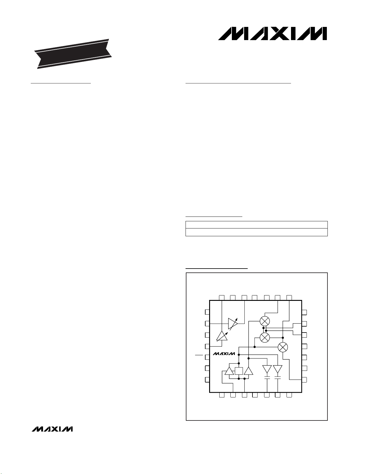
N.C.
GND
LO/2
LOIN
GND
PLOOUT
CLOOUT
CMIXIN
CLNAOUT
GND
PLNAOUT
GND
GND
PMIXIN
GND
CLNAIN
LIN
GAIN
PLNAIN
RLNA
IF-
GND
BUFFEN
V
CC
FMOUT
IF+
RBIAS
QFN
TOP VIEW
÷2
BAND
19-1807; Rev 1; 3/01
EVALUATION KIT
AVAILABLE
Ordering Information
28 QFN
PIN-PACKAGETEMP RANGE
-40°C to +85°CMAX2338EGI
PART
Pin Configuration/
Functional Diagram
Typical Operating Circuit appears at end of data sheet.
For pricing, delivery, and ordering information, please contact Maxim/Dallas Direct! at
1-888-629-4642, or visit Maxim’s website at www.maxim-ic.com.
Page 2
MAX2338
Triple/Dual-Mode CDMA LNA/Mixers
2 _______________________________________________________________________________________
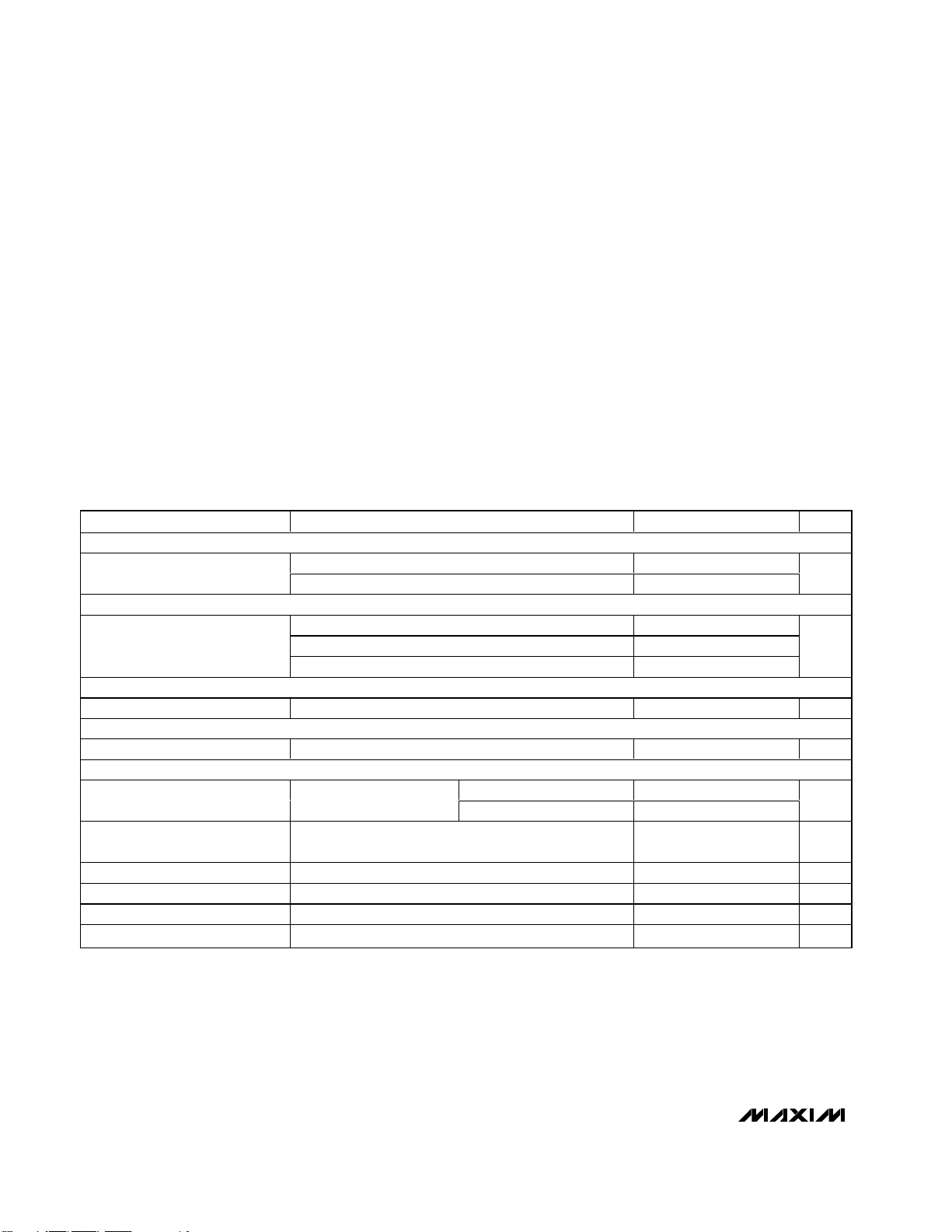
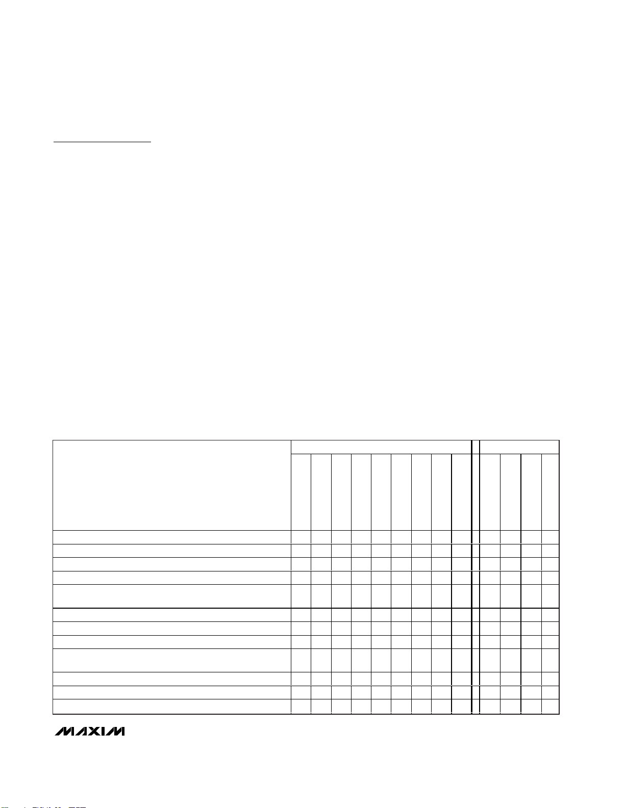
ABSOLUTE MAXIMUM RATINGS
DC ELECTRICAL CHARACTERISTICS
(VCC= +2.7V to +3.3V, R
RBIAS
= R
RLNA
= 24kΩ, BUFFEN = LOW, all RF and IF outputs connected to VCC, no RF applied, TA= -40°C
to +85°C. Typical values are at +3.0V and T
A
= +25°C, unless otherwise noted. Refer to Operational Modes table for control logic.)
Stresses beyond those listed under “Absolute Maximum Ratings” may cause permanent damage to the device. These are stress ratings only, and functional
operation of the device at these or any other conditions beyond those indicated in the operational sections of the specifications is not implied. Exposure to
absolute maximum rating conditions for extended periods may affect device reliability.
VCCto GND..........................................................+0.3V to +4.3V
Digital Input Voltage to GND......................-0.3V to (V
CC
+ 0.3V)
LNA Input Level...............................................................1V peak
LO, Mixer Input Levels .....................................................+5dBm
Digital Input Current .........................................................±10mA
Continuous Power Dissipation (T
A
= +70°C)
28-Pin QFN (derate 28.5mW/°C above T
A
= +70°C).........2W
Operating Temperature Range ...........................-40°C to +85°C
Junction Temperature......................................................+150°C
Storage Temperature Range .............................-65°C to +150°C
Lead Temperature (soldering, 10s) ................................ +300°C
PARAMETER CONDITIONS
UNITS
PCS CDMA MODES
High-gain, low-linearity mode 18 24
Operating Supply Current
High-gain, high-linearity mode 25 33
mA
CELLULAR CDMA MODE
Low-gain mode
25
High-gain, low-linearity mode 18 24
Operating Supply Current
High-gain, high-linearity mode 28 35
mA
FM MODE
Operating Supply Current
17 mA
SHUTDOWN MODE
Shutdown Supply Current 0.1 5 µA
ALL MODES
LO/2 = LOW 7.2 9.5
LO Buffer Supply Current BUFFEN = HIGH
LO/2 = HIGH
mA
Additional Operational Current
Divider Active
Cellular and FM mode; LO/2 = HIGH 1.2 mA
Digital Input Logic High 2.0 V
Digital Input Logic Low 0.6 V
Digital Input High Current 5 µA
Digital Input Low Current -25 µA
MIN TYP MAX
19.5
13.5
10.3
Page 3
MAX2338
Triple/Dual-Mode CDMA LNA/Mixers
_______________________________________________________________________________________ 3
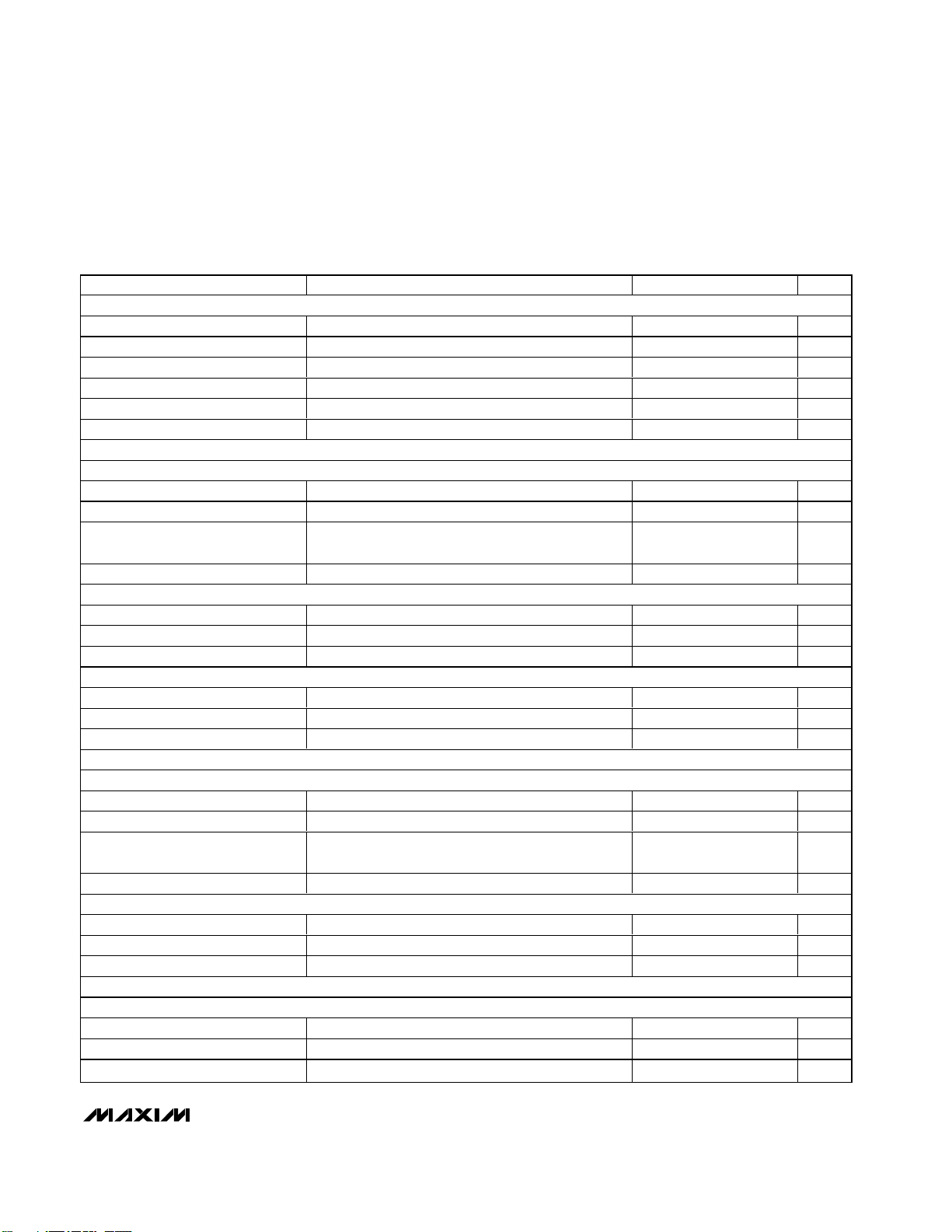
AC ELECTRICAL CHARACTERISTICS
(MAX2338 EV kit, VCC= +2.7V to +3.3V, f
PLNAIN
= f
PMIXIN
= 1930MHz to 1990MHz, f
CLNAIN
= f
CMIXIN
= 869MHz to 894MHz, fIF=
183MHz, high side LO, LO/2 = LOW. All ports matched to 50Ω, R
RLNA
= R
RBIAS
= 24kΩ, TA= -40°C to +85°C. Typical values are at
T
A
= +25°C, VCC= +3.0V, unless otherwise noted.)
PARAMETER CONDITIONS
MIN
TYP
MAX
UNITS
OVERALL PERFORMANCE
Low-Band RF Frequency Range
894
MHz
High-Band RF Frequency Range
MHz
Low-Band LO Frequency Range After divider if active (Note 1)
MHz
High-Band LO Frequency Range (Note 1)
MHz
IF Frequency Range (Note 1) 80 220
MHz
LO Input Level -7 -3 0
dBm
CELLULAR LNA PERFORMANCE
HIGH-GAIN, HIGH-LINEARITY MODES
Gain (Note 2)
dB
Noise Figure (Note 3) TA = +25°C 1.4 1.6 dB
Noise Figure Change Due to
Temperature
T
A
= +25°C to T
MAX
0.3 dB
IIP3 (Notes 3, 4) 9.5 12
dBm
CDMA HIGH-GAIN, LOW-LINEARITY MODE AND FM MODE
Gain (Note 2) 13
dB
Noise Figure (Note 3) TA = +25°C 1.4 1.7 dB
IIP3 (Note 3, 4) 2.5 5.5
dBm
CDMA LOW-GAIN MODE
Gain (Note 2)
0
dBm
Noise Figure (Note 3) 56dB
IIP3 (Notes 3, 4) 15 18
dBm
PCS LNA PERFORMANCE
CDMA HIGH-GAIN, HIGH-LINEARITY MODE
Gain (Note 2)
dB
Noise Figure (Note 3) TA = +25°C 1.4 1.7 dB
Noise Figure Change Due to
Temperature
T
A
= +25°C to T
MAX
0.3 dB
IIP3 (Notes 3, 5) 5.0 7.7
dBm
CDMA HIGH-GAIN, LOW-LINEARITY MODE
Gain (Note 2)
dB
Noise Figure (Note 3) TA = +25°C 1.4 1.7 dB
IIP3 (Notes 3, 5) 2.5 7.5
dBm
CELLULAR MIXER PERFORMANCE
CDMA HIGH-GAIN, HIGH-LINEARITY, AND LOW-GAIN MODES
Gain (Note 2)
dB
Noise Figure (Note 3) TA = +25°C 7.8 9.0 dB
IIP3 (Note 4) 3.0 5.5
dBm
869
1930 1990
950 1100
1750 2210
14.0 15.7 17.0
14.7 16.5
-4.0 -2.3
13.8 15.3 16.9
13.0 14.5 16.5
10.3 13.3 16.4
Page 4
MAX2338
Triple/Dual-Mode CDMA LNA/Mixers
4 _______________________________________________________________________________________
PARAMETER CONDITIONS
MIN
TYP
MAX
UNITS
HIGH-GAIN, LOW-LINEARITY IDLE MODE
Gain (Note 2)
13 16 dB
Noise Figure (Note 3) TA = +25°C 7.3 9.0 dB
IIP3 (Notes 3, 4) 1.4 3.5
dBm
FM MODE
Gain (Note 2) 6.0 8.8
dB
Noise Figure (Note 3) TA = +25°C 8.7
dB
IIP3 (Note 4) 1.4 3.4
dBm
PCS MIXER PERFORMANCE
CDMA HIGH-GAIN, HIGH-LINEARITY MODE
Gain (Note 2)
17 dB
Noise Figure (Note 3) TA = +25°C 7.8 9.0 dB
IIP3 (Notes 3, 5) 3.5 7.5
dBm
HIGH-GAIN, LOW-LINEARITY MODE
Gain (Note 2)
14
dB
Noise Figure (Note 3) TA = +25°C 7.2 9.0 dB
IIP3 (Note 5) 0.5 2.5
dBm
ALL MODES
Mixer Output 1dB Compression -1
dBm
4 x 5 Suppression (Note 6)
dB
2 x 2 Inp ut Inter cep t P oi nt ( N otes 3, 7)
25 33
dBm
LO Output Level (Note 3) Into 50Ω or 100Ω load, BUFFEN = HIGH -12 -6
dBm
LO Output Leakage BUFFEN = LOW -35
dBm
LO E m i ssi on at P C S LN A Inp ut P or t -55
dBm
LO Emission at Cellular LNA Input
Port
-55
dBm
LO Output Harmonic Suppression BUFFEN = HIGH -15
dBc
PCS band, 80MHz below LO
LO Output Noise Power BUFFEN = HIGH
C ell ul ar b and , 45M Hz b el ow LO
dBm/Hz
RF Ports Return Loss
All active RF ports including 2-element matching
10 dB
AC ELECTRICAL CHARACTERISTICS (continued)
(MAX2338 EV kit, VCC= +2.7V to +3.3V, f
PLNAIN
= f
PMIXIN
= 1930MHz to 1990MHz, f
CLNAIN
= f
CMIXIN
= 869MHz to 894MHz, fIF=
183MHz, high side LO, LO/2 = LOW. All ports matched to 50Ω, R
RLNA
= R
RBIAS
= 24kΩ, TA= -40°C to +85°C. Typical values are at
T
A
= +25°C, VCC= +3.0V, unless otherwise noted.)
Note 1: Operation over this frequency range may require the ports to be rematched for the desired operating frequency.
Note 2: MIN guaranteed by production test, MAX guaranteed by design and characterization.
Note 3: Guaranteed by design and device characterization.
Note 4: Two-tone IIP3. Tested at f
RF1
= 880MHz, f
RF2
= 880.9MHz, and power = -25dBm/tone.
Note 5: Two-tone IIP3. Tested at f
RF1
= 1960MHz, f
RF2
= 1961.25MHz, and power = -25dBm/tone.
Note 6: F
LO
= 1064MHZ, f
RF1
= 887.8MHz at -30dBm, f
RF2
= 881MHz at -100dBm. Performance is measured as P
IF
due to
RF1 - P
IF
due to RF2.
Note 7: F
LO
= 2143MHz, f
RF1
= 2051.5MHz at -35dBm, f
RF2
= 1960MHz at -100dBm. Performance is measured as P
IF
due to
RF1 - P
IF
due to RF2.
10.1
11.1
11.0
11.7 14.5
11.2
>45
-161
-161
16.2
Page 5

_______________________________________________________________________________________ 5
MAX2338
Triple/Dual-Mode CDMA LNA/Mixers
Typical Operating Characteristics
(TA = +25°C, unless otherwise noted.)
0
10
5
20
15
25
30
-50 0 50 100
PCS-BAND SUPPLY CURRENT
MAX2338 toc01
TEMPERATURE (°C)
SUPPLY CURRENT (mA)
HGHL
HGLL
-5
0
10
5
15
20
850 870860 880 890 900
CELLULAR-BAND LNA GAIN
vs. FREQUENCY
MAX2338 toc05
FREQUENCY (MHz)
GAIN (dB)
HGHL
HGLL, FM
LGHL
7
10
9
8
11
12
13
14
15
16
17
1900 19401920 1960 1980 2000
PCS-BAND LNA GAIN
vs. FREQUENCY
MAX2338 toc06
FREQUENCY (MHz)
GAIN (dB)
HGHL
HGLL
2
6
4
10
8
12
14
48106121416
CELLULAR-BAND HGHL LNA IIP3
vs. CURRENT
MAX2338 toc08
LNA CURRENT (mA)
IIP3 (dBm)
TA = +85°C
TA = -40°C
TA = +25°C
1.2
1.4
1.3
1.5
1.8
1.9
1.7
1.6
2.0
1900 1920 1940 1960 1980 2000
MAX2338 toc09
FREQUENCY (MHz)
NOISE FIGURE (dB)
PCS-BAND HGHL LNA NOISE FIGURE
vs. FREQUENCY
15mA
8.4mA
4mA
12
17
18
486 101214161820
CELLULAR-BAND HGHL LNA GAIN
vs. CURRENT
MAX2338 toc04
LNA CURRENT (mA)
13
GAIN (dB)
14
15
16
TA = -40°C
TA = +85°C
TA = +25°C
2
3
4
5
6
7
8
9
10
456789
PCS-BAND HGHL LNA IIP3
vs. CURRENT
MAX2338 toc07
LNA CURRENT (mA)
IIP3 (dBm)
TA = -40°C
TA = +25°C
TA = +85°C
0
10
5
20
15
25
30
-50 0 50 100
CELLULAR-BAND SUPPLY CURRENT
MAX2338 toc02
TEMPERATURE (°C)
SUPPLY CURRENT (mA)
HGHL
LGHL
HGLL
FM
10
12
11
14
13
16
15
17
48106 121416
PCS-BAND HGHL LNA GAIN
vs. CURRENT
MAX2338 toc03
LNA CURRENT (mA)
GAIN (dB)
TA = +25°C
TA = +85°C
TA = -40°C
Page 6

MAX2338
Triple/Dual-Mode CDMA LNA/Mixers
6 _______________________________________________________________________________________
Typical Operating Characteristics (continued)
(TA = +25°C, unless otherwise noted.)
0
0.6
0.4
0.2
0.8
1.0
1.2
1.4
1.6
1.8
2.0
840 860850 870 880 890 900
MAX2338 toc10
FREQUENCY (MHz)
NOISE FIGURE (dB)
CELLULAR-BAND HGHL LNA NOISE
FIGURE vs. FREQUENCY
16mA
11mA
6mA
10
12
11
14
13
15
16
-20 -10-15 -5 0 5
PCS-BAND MIXER CONVERSION GAIN
vs. LO INPUT LEVEL
MAX2338 toc14
LO INPUT LEVEL (dBm)
GAIN (dB)
HIGH SIDE LO HGHL
LOW SIDE LO HGHL
8
9
10
11
12
13
14
-20 -16-18 -14 -12 -10 -8 -6
CELLULAR-BAND MIXER CONVERSION
GAIN vs. RF INPUT LEVEL
MAX2338 toc15
RF INPUT LEVEL (dBm)
GAIN (dB)
-6
-4
0
-2
4
6
2
8
481061214
CELLULAR-BAND HGHL MIXER IIP3
vs. CURRENT
MAX2338 toc17
MIXER CURRENT (mA)
IIP3 (dB)
TA = +85°C
TA = +25°C
TA = -40°C
4681012
PCS-BAND HGHL MIXER IIP3
vs. CURRENT
MAX2338 toc18
MIXER CURRENT (mA)
-6
-4
-2
0
2
4
IIP3 (dB)
6
8
HIGH SIDE LO, TA = +25°C
HIGH SIDE LO, TA = +85°C
HIGH SIDE LO, TA = -40°C
14
13
12
11
10
-20 -10-15 -5 0 5
CELLULAR-BAND MIXER CONVERSION
GAIN vs. LO INPUT LEVEL
MAX2338 toc13
LO INPUT LEVEL (dBm)
GAIN (dB)
HGHL
HGLL
MAX2338 toc16
8
10
14
12
16
18
-20 -16 -14-18 -12 -10 -8 -6
PCS-BAND MIXER CONVERSION GAIN
vs. RF INPUT LEVEL
RF INPUT LEVEL (dBm)
GAIN (dB)
HIGH SIDE LO HGHL
LOW SIDE LO HGHL
6
10
8
14
12
16
18
4101268 14
CELLULAR-BAND HGHL MIXER
CONVERSION GAIN vs. CURRENT
MAX2338 toc11
MIXER CURRENT (mA)
CONVERSION GAIN (dB)
TA = -40°C
TA = +25°C
TA = +85°C
6
9
8
7
10
11
12
13
14
15
16
PCS-BAND MIXER
CONVERSION GAIN vs. CURRENT
MAX2338 toc12
4101268 14
MIXER CURRENT (µA)
CONVERSION GAIN (dB)
TA = -40°C, HIGH SIDE LO
TA = +25°C, HIGH SIDE LO
TA = -40°C, LOW SIDE LO
TA = +85°C, LOW SIDE LO
TA = +85°C, HIGH SIDE LO
TA = +25°C, LOW SIDE LO
Page 7

_______________________________________________________________________________________ 7
MAX2338
Triple/Dual-Mode CDMA LNA/Mixers
Typical Operating Characteristics (continued)
(TA = +25°C, unless otherwise noted.)
5.0
5.5
6.0
6.5
7.0
7.5
8.0
8.5
9.0
850 860 870 880 890 900
CELLULAR-BAND MIXER NOISE FIGURE
vs. RF FREQUENCY
MAX2338 toc19
RF FREQUENCY (MHz)
NOISE FIGURE (dB)
FM
HGHL
HGLL
PARALLEL RESISTANCE (kΩ)
0
20
10
40
30
50
60
0 200100 300 400 500
FM MIXER IF PORT DIFFERENTIAL
PORT IMPEDANCE
MAX2338 toc23
RF FREQUENCY (MHz)
PARALLEL RESISTANCE (kΩ)
0
1.0
0.5
2.0
1.5
2.5
3.0
CAPACITANCE
RESISTANCE
-80
-60
-70
-50
-20
-10
-30
-40
0
-15 -10 -5 0 5
PCS-BAND LO BUFFER OUTPUT LEVEL
vs. INPUT LEVEL
MAX2338 toc24
LO INPUT LEVEL (dBm)
OUTPUT LEVEL (dBm)
LO
2 X LO
3 X LO
0 200100 300 400
0
15
45
30
60
75
500
CDMA MIXER IF PORT DIFFERENTIAL
PORT IMPEDANCE
MAX2338 toc22
RF FREQUENCY (MHz)
PARALLEL RESISTANCE (kΩ)
0
0.4
1.2
0.8
1.6
2.0
PARALLEL RESISTANCE (kΩ)
CAPACITANCE
RESISTANCE
5.0
5.5
6.0
6.5
7.0
7.5
8.0
8.5
9.0
1920 1940 1960 1980 2000
PCS-BAND MIXER
NOISE FIGURE vs. RF FREQUENCY
MAX2338 toc20
RF FREQUENCY (MHz)
NOISE FIGURE (dB)
HGHL LOW SIDE LO
HGLL LOW SIDE LO
HGHL HIGH SIDE LO
HGLL HIGH SIDE LO
OUTPUT LEVEL (dBm)
0
-10
-20
-30
-40
-15 -5-10 0 5
CELLULAR-BAND LO BUFFER
OUTPUT LEVEL vs. INPUT LEVEL
MAX2338 toc21
LO INPUT LEVEL (dBm)
LO / 2
2 X LO / 2
3 X LO / 2
Page 8

MAX2338
Triple/Dual-Mode CDMA LNA/Mixers
8 _______________________________________________________________________________________
Pin Description
PIN NAME FUNCTION
1 RLNA
LNA Bias–Setting Resistor Connection. For nominal bias, connect a 24kΩ resistor to ground. The
value of this resistor sets the bias current for HGHL LNAs.
2 PLNAIN
High-Band RF Input. Requires a blocking capacitor which may be used as part of the input
matching network.
3, 8, 11, 18,
24, 25, 27,
Exposed
Paddle
GND
Ground Reference for RF, DC and Logic Inputs. Solder the exposed paddle evenly to the circuit
board ground plane.
4 CLNAIN
Low-Band RF Input. Requires a blocking capacitor which may be used as part of the input
matching network.
5 BAND Band-Select Logic Input. LOW selects high-band (PCS), HIGH selects low-band (cellular).
6 LIN Linearity-Select Logic Input. See Detailed Description for control modes.
7 GAIN Gain-Select Logic Input. See Detailed Description for control modes.
9 LO/2
LO Divider-Select Input. LOW disables LO divider, HIGH selects divider in cellular and FM
modes. See Detailed Description for control modes.
10 LOIN LO Input Port. Requires an external DC blocking capacitor.
12 PLOOUT
PCS LO Buffer Output Port. Internally matched to 100Ω (nominal). Does not require a blocking
capacitor.
13 CLOOUT
Cell LO Buffer Output Port. Internally matched to 100Ω (nominal). Does not require a blocking
capacitor. The output frequency is one half LOIN when LO/2 is floating or HIGH, and equal to
LOIN when LO/2 is LOW.
14 NC No Connection
15 FMOUT
FM Mixer Output Port. Requires pullup inductor and DC blocking capacitor, which may be used
as part of the output matching network.
16 V
CC
Power Supply Pin. Bypass with capacitor as close to the pin as possible.
17 BUFFEN
LO Output Buffer Enable. Drive BUFFEN HIGH to power up the LO output buffer associated with
the selected band.
19, 20 IF-, IF+
Mixer Differential Outputs. Require pullup inductors and series capacitors which can be used as
part of the output matching network.
21 RBIAS
Bias Setting Resistor Connection. For nominal bias, connect a 24kΩ resistor to ground. The value
of this resistor sets current for all blocks except HGHL LNA.
22 CMIXIN
Low-Band Mixer Input. Requires a blocking capacitor which may be used as part of the input
matching network.
23 PMIXIN
High-Band Mixer Input. Requires a blocking capacitor which may be used as part of the input
matching network.
26
High-Band LNA Output Port. Connect a pullup inductor to VCC and an external series blocking
capacitor which may be used as a part of the output matching network.
28
Low-Band LNA Output Port. Connect a pullup inductor to VCC and an external series blocking
capacitor which may be used as a part of the output matching network.
PLNAOUT
CLNAOUT
Page 9
MAX2338
Triple/Dual-Mode CDMA LNA/Mixers
_______________________________________________________________________________________ 9
Detailed Description
The MAX2338 consists of cellular band and PCS band
(LNAs) and mixers. The IC also consists of a local oscillator (LO) divider and LO buffers for cellular and PCS
bands.
Low-Noise Amplifiers
The MAX2338 LNAs’ gain and linearity are switched by
the GAIN and LIN input, respectively. The PCS band
LNA has two operational modes: high-gain high-linearity
(HGHL) and high-gain low-linearity (HGLL). The cellular
band LNA has three operational in modes: HGHL, HGLL,
and low-gain high-linearity (LGHL) modes. The table in
the Operational Modes section shows the pin settings for
BAND, GAIN, and LIN for various operating modes. Use
HGHL mode when extra high linearity is required for
cross-modulation suppression, HGLL mode when the
transmitter is off and cross-modulation is not a concern,
and LGHL mode when receiving large signals.
Downconverter
The downconverters in these devices are double balanced mixers. The PCS band mixer and digital cellular
band mixer share the same IF output ports. The cellular
FM band mixer has its own IF output to feed to a different
filter. When the linearity requirement is high, the LIN control input increases the current in the downconverter. The
downconverter requires a DC blocking capacitor at the
input and output, and a pullup inductor at the output. The
DC blocking capacitors can be designed to be part of
the matching circuits. The table in the Operational
Modes section shows the settings for BAND, GAIN, and
LIN for various operating modes.
LO Output Buffers
There are two LO output buffers: cellular and PCS. The
inputs are tied together and internally matched to 50Ω.
The outputs of the PCS and cellular buffers are brought
out separately. The outputs of the buffers are internally
matched and include a DC blocking capacitor.
LO Divider
The MAX2338 includes an LO divider circuit which
enables a single VCO for both cellular and PCS bands.
The LO/2 logic input turns the divider on or off in the cellular band.
FUNCTION CONTROL PIN
MODES
BAND (H/L)
LOX1
LO /2
HGHL Amp
HGLL Amp
LGHL Amp
CDMA HL Mixer
CDMA LL Mixer
FM Mixer
BAND
GAIN
LIN
LO/2
PCS Band, High-Gain, High-Linearity (HGHL)
X
PCS Band, High-Gain, Low-Linearty (Idle Mode) (HGLL)
X
Undefined
X
Cellular Band CDMA, High-Gain, High-Linearity (HGHL)
1
Cellular Band CDMA, High-Gain, Low-Linearity (Idle Mode)
(HGLL)
1
Cellular Band, CDMA, Low-Gain
1
Cellular Band, FM Mode
1
Cellular Band CDMA, High-Gain, High-Linearity (HGHL)
0
Cellular Band CDMA, High-Gain, Low-Linearity (Idle Mode)
(HGLL)
0
Cellular Band, CDMA, Low-Gain
0
Cellular Band, FM Mode
0
Shutdown
X
Table 1. Operational Modes
H ✓✓ ✓ 011
H ✓✓✓010
————————— 001
L ✓✓ ✓ 111
L ✓✓ ✓ 110
L ✓✓✓ 101
L ✓✓ ✓100
L ✓✓ ✓ 111
L ✓✓✓110
L ✓✓✓101
L ✓✓ ✓100
000
Page 10

MAX2338
Triple/Dual-Mode CDMA LNA/Mixers
10 ______________________________________________________________________________________
Operational Modes
The various operating modes are controlled by the logic
inputs BAND, GAIN, LIN, and LO/2. Table 1 shows the
pin settings for the various operating modes.
Applications Information
Cascaded LNA/Mixer Performance
The LNA and mixer design optimizes cascaded performance in all gain and linearity modes. In HGHL mode
both the LNA and mixer have a low noise figure, high
gain, and high linearity. The LNA has high gain to mini-
mize the noise contribution of the mixer, thus increasing
the receiver’s sensitivity, and the LNA has high linearity
for cross-modulation suppression. The HGLL mode is
used when the transmitter is off and cross-modulation is
not a concern. In LGHL mode, the received signal is
strong enough that linearity is the primary concern. The
LNA gain is reduced for higher system linearity.
S-Parameters
Use the S-parameters listed in the following tables to
design the RF matching circuits.
FREQUENCY (MHz) |S11| ∠S11 |S21| ∠S21 |S12| ∠S12 |S22| ∠S22
30 0.905 -5.4 0.145 -38 0.002 -55 0.98 -47
50 0.899 -8.1 0.467 -57 0.003 -126 0.94 -72
100 0.891 -15.1 1.34 -86 0.012 -174 0.96 -117
150 0.884 -21.8 2.2 -108 0.023 176 0.96 -144
200 0.874 -28.2 2.83 -127 0.027 165.8 0.95 -162
300 0.85 -41.6 3.77 -157.5 0.029 137 0.93 -172
400 0.818 -52.5 4.24 178.3 0.030 127 0.90 155
500 0.785 -63.5 4.44 155.4 0.036 112 0.94 129
600 0.75 -71.6 4.38 140 0.040 98 0.87 100
700 0.714 -79.8 4.16 125 0.048 90 0.84 78
800 0.683 -76.5 4.03 112.6 0.059 83.0 0.793 67.5
810 0.681 -77.0 4.01 111.2 0.060 82.8 0.798 66.5
820 0.677 -77.0 3.99 110.0 0.061 82.0 0.800 65.7
830 0.675 -78.0 3.97 108.5 0.061 80.9 0.799 65.0
840 0.670 -78.3 3.96 107.2 0.062 80.6 0.792 64.2
850 0.668 -78.8 3.93 106.4 0.063 79.2 0.782 63.4
860 0.665 -79.0 3.92 104.7 0.063 78.1 0.769 62.7
870 0.661 -79.5 3.91 103.4 0.063 77.2 0.753 61.8
880 0.660 -80.0 3.89 102.1 0.063 76.5 0.733 60.6
890 0.660 -80.4 3.87 100.8 0.063 75.4 0.710 59.4
900 0.653 -81.0 3.86 99.3 0.063 73.5 0.690 57.7
1000 0.614 -97.0 3.59 86.2 0.07 20 0.680 51.8
1250 0.547 -111 3.15 60.8 0.09 -13.2 0.650 37
1500 0.457 -131 2.93 34 0.109 -36 0.610 15.9
1750 0.310 -164 2.48 18 0.14 -62 0.580 -9.6
2000 0.320 166 2.1 -40 0.185 -98 0.490 -33
2500 0.300 141 1.62 -41 0.19 -150 0.360 -70
3000 0.310 122 1.29 -66 0.19 136 0.41 -64
3500 0.360 86 1.18 -88 0.2 90 0.500 -61
4000 0.360 10 1.14 -112 0.2 43 0.480 -50
Table 2. MAX2338 Cellular Band LNA S-parameters High-Gain, High-Linearity Mode
Page 11

MAX2338
Triple/Dual-Mode CDMA LNA/Mixers
______________________________________________________________________________________ 11
Layout Considerations
Keep RF signal lines as short as possible to minimize
losses and radiation. Use high Q components for the
LNA input-matching circuit to achieve the lowest possible noise figure. At the digital mixer outputs, keep the
differential signal lines together and of equal length to
ensure signal balance. For best gain and noise performance, solder the exposed paddle evenly to the board
ground plane.
FREQUENCY (MHz) |S11| ∠S11 |S21| ∠S21 |S12| ∠S12 |S22| ∠S22
30 0.890 -4.9 0.002 -95 0.001 -112 0.996 -48
50 0.883 -7.2 0.001 -60 0.001 -121 0.990 -73
100 0.872 -13.2 0.391 -81 0.002 -178 0.980 -114
200 0.841 -25 0.882 -112 0.007 171 0.970 -150
300 0.799 -35 1.42 -131 0.010 150 0.959 -166
400 0.778 -41 2.1 -153 0.02 125 0.947 -173
600 0.750 -62 2.15 -172 0.02 100 0.943 173
800 0.706 -75 2.2 162 0.025 80 0.944 151
1000 0.676 -85 2.45 150 0.029 65 0.919 133
1200 0.659 -94 2.59 142 0.032 42 0.879 115
1500 0.634 -108 3.03 134 0.036 31 0.824 94.4
1750 0.578 -110 3.58 126 0.038 19 0.780 81
1900 0.560 -90.8 3.64 120.6 0.04 11.8 0.740 61.7
1910 0.558 -91.0 3.64 119.6 0.04 9.06 0.738 60.7
1920 0.554 -91.4 3.64 118.9 0.04 8.8 0.733 59.6
1930 0.551 -91.7 3.63 118.2 0.04 6.7 0.729 58.5
1940 0.547 -92.2 3.63 117.7 0.04 5.3 0.725 57.4
1950 0.543 -92.2 3.63 117.0 0.04 4.87 0.720 56.1
1960 0.538 -92.4 3.63 116.5 0.04 4.1 0.716 55.0
1970 0.536 -92.5 3.61 115.9 0.04 1.8 0.716 53.6
1980 0.533 -92.9 3.60 115.2 0.04 1.5 0.711 52.3
1990 0.530 -93.0 3.59 114.7 0.04 0 0.707 50.9
2000 0.523 -93.4 3.57 113.0 0.04 -2.1 0.702 49.5
2250 0.347 -155 2.88 131 0.05 -32 0.518 24
2500 0.298 -158 2.71 172 0.05 -72 0.489 5
3000 0.273 -160 2.64 -165 0.06 -94 0.473 -18
4000 0.245 -170 2.03 -145 0.067 -120 0.425 -30
Table 3. MAX2338 PCS Band LNA S-Parameters High-Gain, High-Linearity Mode
Page 12

MAX2338
Triple/Dual-Mode CDMA LNA/Mixers
12 ______________________________________________________________________________________
Table 5. MAX2338 PCS Band Mixer Input
S-Parameters High-Gain, High-Linearity
Mode
Table 4. MAX2338 Cellular Band Mixer
Input S-Parameters High-Gain, HighLinearity Mode
FREQUENCY
(MHz)
|S11| ∠S11
800 0.843 -67.5
810 0.843 -68.2
820 0.842 -68.8
830 0.842 -69.5
840 0.843 -70.2
850 0.843 -71.0
860 0.843 -71.6
870 0.843 -72.4
880 0.842 -73.0
890 0.841 -74.0
900 0.840 -75.0
FREQUENCY
(MHz)
1900 0.762 -76.9
1910 0.759 -77.8
1920 0.755 -79.0
1930 0.752 -80.1
1940 0.747 -81.2
1950 0.744 -82.2
1960 0.741 -83.2
1970 0.739 -84.3
1980 0.734 -85.5
1990 0.730 -86.7
2000 0.723 87.9
|S11| ∠S11
Page 13

MAX2338
Triple/Dual-Mode CDMA LNA/Mixers
811 14
N.C.
16
17
18
21
GAIN
LIN
BUFFEN
1
3
5
6
7
CELLULAR
PCS
CELL
PCS
CDMA
V
CC
V
CC
V
CC
24kΩ
FM
PCS LO LO_OUT
LO/2
BAND
20Ω
MAX2338
÷2
28
27
26
25 24
23
22
2
4
13
12
109
15
19
20
7pF
100pF
15nH
6800pF
2.7nH
0.01µF
0.75pF
2.7pF
8.2nH
2.7nH
100pF
6800pF
2.2nH
6800pF
3.9nH
22pF
4.7pF
120nH
8.25kΩ
1%
100pF
3.3kΩ
4pF
4pF
120nH
120nH
24kΩ
Typical Operating Circuit
Package Information
For the latest package outline information, go to
www.maxim-ic.com/packages.
Maxim cannot assume responsibility for use of any circuitry other than circuitry entirely embodied in a Maxim product. No circuit patent licenses are
implied. Maxim reserves the right to change the circuitry and specifications without notice at any time.
Maxim Integrated Products, 120 San Gabriel Drive, Sunnyvale, CA 94086 408-737-7600 ____________________ 13
© 2002 Maxim Integrated Products Printed USA is a registered trademark of Maxim Integrated Products.
 Loading...