

Page 1
现货库存、技术资料、百科信息、热点资讯,精彩尽在鼎好!
General Description
The MAX2335 RF front-end receiver IC is designed for
CDMA and OFDM applications in the 450MHz band.
The MAX2335 includes a low-noise amplifier (LNA) with
adjustable IIP3 to minimize desensitization due to crossmodulation in the presence of a large interfering signal.
The mixer features differential IF outputs and is
designed for high linearity and low noise, which is well
suited for CDMA and OFDM applications.
An on-chip frequency divider is included to allow the
use of a standard 1GHz VCO. Alternatively, the divider
can be bypassed for use with a lower-frequency VCO.
The MAX2335 is available in a 28-pin TQFN package
with exposed paddle and is specified for the -40°C to
+85°C extended temperature range. The device is also
offered in a lead-free package.
Features
♦ 1.5dB LNA Noise Figure
♦ 16dB LNA Gain
♦ 2.1dB Cascaded Noise Figure
♦ Adjustable LNA IIP3
♦ LO Output Buffer for Transmitter
♦ LO Frequency Divider
♦ Small 5mm x 5mm, 28-Pin (Lead-Free) TQFN
Package
MAX2335
450MHz CDMA/OFDM LNA/Mixer
________________________________________________________________ Maxim Integrated Products 1
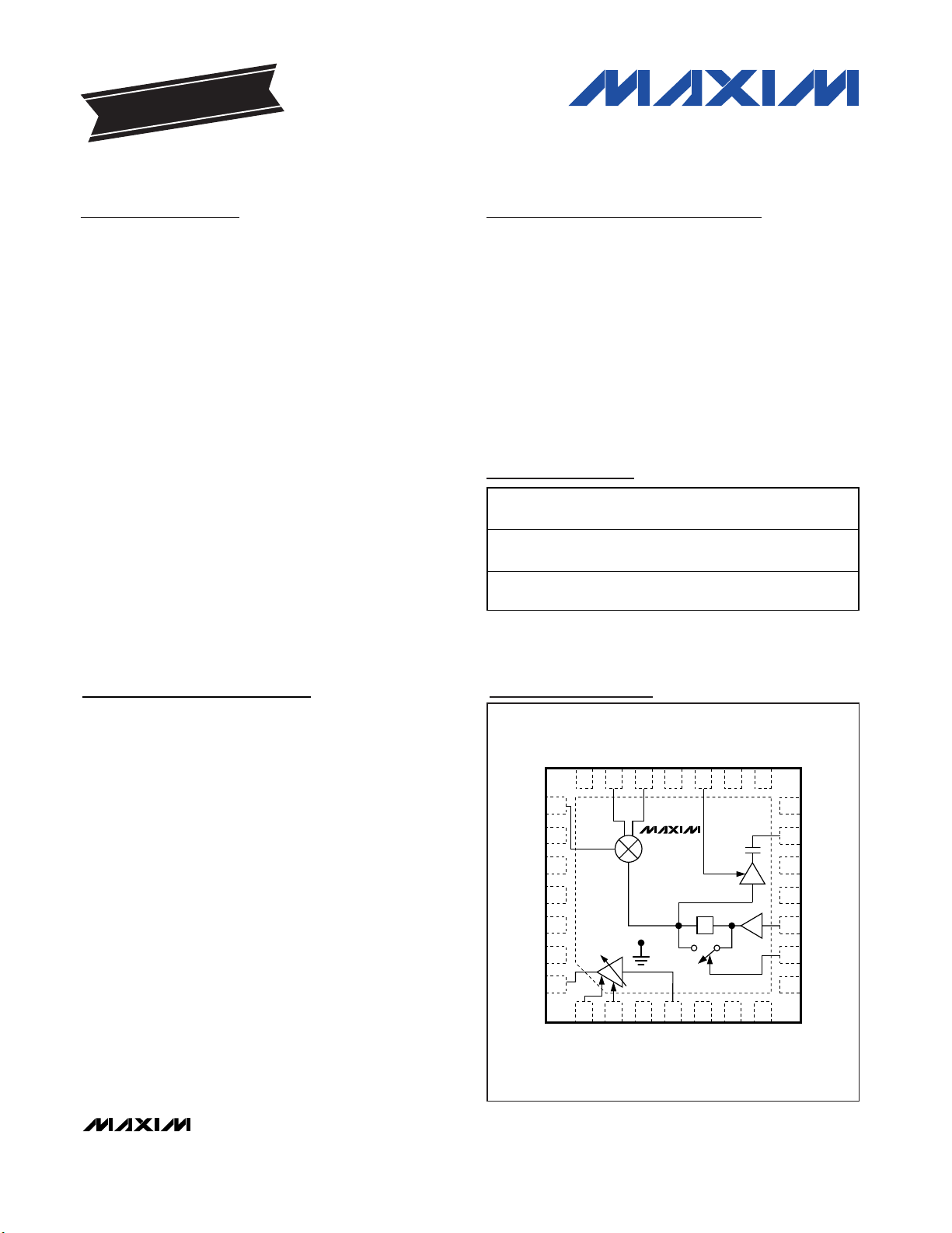
MAX2335
TOP VIEW
÷2
THIN QFN
5mm x 5mm
26
27
25
24
10
9
11
R
LNA
LNAIN
MODEO
MODE1
MODE2
12
DEGEN
IF_CDMA+
N.C.
BUFFEN
EP
R
BIAS
VCCV
CC
12
N.C.
4567
2021 19 17 16 15
V
CC
N.C.
I.C.
N.C.
LO_IN
LO/2
GND
IF_CDMA-
3
18
28
8
LNAOUT
N.C.
N.C.
23
13
LO_OUT
I.C.
22
14
N.C.
MIXIN
+
Pin Configuration/
Functional Diagram
Ordering Information
19-0492; Rev 0; 10/05
For pricing, delivery, and ordering information, please contact Maxim/Dallas Direct! at
1-888-629-4642, or visit Maxim’s website at www.maxim-ic.com.
*EP = Exposed paddle.
+Denotes lead-free package.
EVALUATION KIT
AVAILABLE
PART
TEMP RANGE
PIN-PACKAGE
PKG
CODE
MAX2335ETI
(5mm x 5mm)
T2855-3
MAX2335ETI+
(5mm x 5mm)
T2855+3
Applications
450MHz-Band, WCDMA, IS-95, IS-2000, OFDM,
Wireless Data Links
-40°C to +85°C
-40°C to +85°C
28 Thin QFN-EP*
28 Thin QFN-EP*
Page 2
MAX2335
450MHz CDMA/OFDM LNA/Mixer
2 _______________________________________________________________________________________
ABSOLUTE MAXIMUM RATINGS
DC ELECTRICAL CHARACTERISTICS
(VCC= +2.9V to +3.3V, R
BIAS
= 18kΩ, R
LNA
= 24kΩ, BUFFEN = LOW, LO/2 = HIGH, TA= -40°C to +85°C, unless otherwise noted.
Typical values are at V
CC
= +2.9V, LOW = 0V, HIGH = +3.0V, TA= +25°C, unless otherwise noted.) (Note 1)
Stresses beyond those listed under “Absolute Maximum Ratings” may cause permanent damage to the device. These are stress ratings only, and functional
operation of the device at these or any other conditions beyond those indicated in the operational sections of the specifications is not implied. Exposure to
absolute maximum rating conditions for extended periods may affect device reliability.
VCCto GND...........................................................-0.3V to +4.3V
All Other Pins to GND.................................-0.3V to (V
CC
+ 0.3V)
AC Input Pins (LNAIN, LO_IN, MIXIN) to GND ...............1V Peak
Continuous Power Dissipation (T
A
= +70°C)
28-Pin Thin QFN (derate 34.5mW/°C above +70°C) ...........2.7W
Operating Temperature Range ...........................-40°C to +85°C
Junction Temperature......................................................+150°C
Storage Temperature Range .............................-65°C to +150°C
Lead Temperature (soldering, 10s) .................................+300°C
CAUTION! ESD SENSITIVE DEVICE
PARAMETER
CONDITIONS
UNITS
HGHL mode (MODE[2:0] = 111) 32 38
HGLL mode (MODE[2:0] = 101) 24 29
Operating Supply Current I
CC
LG mode (MODE[2:0] = 011) 27 31
mA
Shutdown Supply Current I
CC
Shutdown mode (MODE[2:0] = 000) 0.2 10 µA
LO Buffer Supply Current I
CC
Addition for BUFFEN = HIGH 7 13 mA
Digital Input-Logic High V
IH
2V
Digital Input-Logic Low V
IL
0.6 V
Digital Input Current (Logic-High)
I
IH
5µA
Digital Input Current (Logic-Low)
I
IL
-25 µA
AC ELECTRICAL CHARACTERISTICS
(MAX2335 EV Kit, VCC= +2.9V to +3.3V, f
LNAIN
= f
MIXIN
= 465MHz, fIF= 110MHz, fLO= 2 x (f
MIXIN
+ fIF), 50Ω system impedance,
R
BIAS
= 18kΩ, R
LNA
= 24kΩ, cascaded performance includes 2dB interstage filter loss, TA= -40°C to +85°C, unless otherwise
noted. Typical values are at V
CC
= +2.9V, P
LO_IN
= -7dBm, LOW = 0V, HIGH = +3.0V, TA= +25°C, unless otherwise noted.)
SYMBOL
MIN TYP MAX
OVERALL PERFORMANCE
RF Frequency Range f
LO Frequency Range f
IF Frequency Range f
LO Input Power (Note 2) -7 -3 0 dBm
LO Buffer Output Power BUFFEN = HIGH -10 -6 dBm
Return Loss
CASCADED PERFORMANCE
HIGH-GAIN, HIGH-LINEARITY MODE (MODE[2:0] = 111)
Gain G (Note 1) 23.0 27 31.5 dB
Noise Figure NF Incl ud i ng off- chi p m atchi ng , TA = + 25°C ( N ote 2) 2.2 2.6 dB
Input Third-Order Intercept Point IIP3 TA = + 25°C (Notes 1, 3) -14 -11.5 dBm
PARAMETER SYMBOL CONDITIONS MIN TYP MAX UNITS
RF
LO
IF
After optional LO/2 500 to 660 MHz
All modes, all active ports, including
2-element matching network, if necessary
420 to 470 MHz
80 to 190 MHz
10 dB
Page 3
MAX2335
450MHz CDMA/OFDM LNA/Mixer
_______________________________________________________________________________________ 3
Note 1: Specifications at TA= +25°C and +85°C are guaranteed by production test. Specifications at TA= -40°C are guaranteed
by design and characterization.
Note 2: Guaranteed by design and characterization.
Note 3: Two-tone IIP3 tested at f
RF1
= 465.9MHz and f
RF2
= 466.7MHz at -25dBm/tone.
AC ELECTRICAL CHARACTERISTICS (continued)
(MAX2335 EV Kit, VCC= +2.9V to +3.3V, f
LNAIN
= f
MIXIN
= 465MHz, fIF= 110MHz, fLO= 2 x (f
MIXIN
+ fIF), 50Ω system impedance,
R
BIAS
= 18kΩ, R
LNA
= 24kΩ, cascaded performance includes 2dB interstage filter loss, TA= -40°C to +85°C, unless otherwise
noted. Typical values are at V
CC
= +2.9V, P
LO_IN
= -7dBm, LOW = 0V, HIGH = +3.0V, TA= +25°C, unless otherwise noted.)
PARAMETER
CONDITIONS
TYP
UNITS
HIGH-GAIN, LOW-LINEARITY MODE (MODE[2:0] = 101)
Gain G (Note 1)
26.5
dB
Noise Figure NF
2.1
dB
Input Third-Order Intercept Point
IIP3 TA = + 25°C (Notes 1, 3)
-12.5
dBm
LOW-GAIN MODE (MODE[2:0] = 011)
Gain G (Note 1) 5 9
dB
Noise Figure NF
12
dB
Input Third-Order Intercept Point
IIP3 TA = + 25°C (Notes 1, 3) 3 7
dBm
LNA PERFORMANCE
HIGH-GAIN, HIGH-LINEARITY MODE (MODE[2:0] = 111)
Gain G
LNA
15.5 dB
Noise Figure
Including off-chip matching 1.7 dB
Input Third-Order Intercept Point
(Note 3) +7
dBm
HIGH-GAIN, LOW-LINEARITY MODE (MODE[2:0] = 101)
Gain G
LNA
14.5 dB
Noise Figure NF
LNA
Including off-chip matching 1.5 dB
Input Third-Order Intercept Point
IIP3
LNA
(Note 3) +5
dBm
LOW-GAIN MODE (MODE[2:0] = 011)
Gain G
LNA
-2.7 dB
Noise Figure
Including off-chip matching 5.5 dB
Input Third-Order Intercept Point
(Note 3) +14
dBm
MIXER PERFORMANCE
HIGH-GAIN, HIGH-LINEARITY MODE (MODE[2:0] = 111)
Gain
14 dB
Noise Figure
Including off-chip matching 7 dB
Input Third-Order Intercept Point
(Note 3) +2
dBm
HIGH-GAIN, LOW-LINEARITY MODE (MODE[2:0] = 101)
Gain
13.5 dB
Noise Figure
Including off-chip matching 6.7 dB
Input Third-Order Intercept Point
(Note 3) 0
dBm
LOW-GAIN MODE (MODE[2:0] = 011)
Gain
14 dB
Noise Figure
Including off-chip matching 7 dB
Input Third-Order Intercept Point
(Note 3) +2
dBm
SYMBOL
IIP3
IIP3
G
NF
IIP3
G
NF
IIP3
G
NF
IIP3
Incl ud i ng off- chi p m atchi ng , TA = + 25°C ( N ote 2)
Incl ud i ng off- chi p m atchi ng , TA = + 25°C ( N ote 2)
NF
LNA
LNA
NF
LNA
LNA
MIXER
MIXER
MIXER
MIXER
MIXER
MIXER
MIXER
MIXER
MIXER
MIN
21.0
MAX
30.5
2.5
-15
14
15
Page 4
MAX2335
450MHz CDMA/OFDM LNA/Mixer
4 _______________________________________________________________________________________
Typical Operating Characteristics
(MAX2335 EV Kit, VCC= +2.9V, f
LNAIN
= 465MHz, fIF= 110MHz, f
LO_IN
= 1150MHz, P
LO_IN
= -7dBm, R
BIAS
= 18kΩ, R
LNA
= 24kΩ,
TA= +25°C, unless otherwise noted.)
SUPPLY CURRENT (HGHL)
vs. TEMPERATURE
MAX2335 toc01
TEMPERATURE (°C)
SUPPLY CURRENT (mA)
603510-15
28
30
32
34
26
-40 85
LNA GAIN VS RF FREQUENCY
MAX2335 toc02
RF FREQUENCY (MHz)
LNA GAIN (dB)
480460440420
-4
0
4
8
12
16
20
-8
400 500
HG
LG
6
4
2
0
400
LG
HG
440420 460 480 500
LNA NOISE FIGURE vs. RF FREQUENCY
MAX2335 toc03
RF FREQUENCY (MHz)
LNA NOISE FIGURE (dB)
5
6
8
7
9
10
-40 10-15 35 60 85
LNA HGHL IIP3 vs. TEMPERATURE
MAX2335 toc04
TEMPERATURE (°C)
LNA HGHL IIP3 (dBm)
R
LNA
= 18kΩ
R
LNA
= 24kΩ
MIXER HGHL IIP3 vs. TEMPERATURE
MAX2335 toc05
TEMPERATURE (°C)
MIXER HGHL IIP3 (dBm)
603510-15
-1
0
1
2
3
4
-2
-40 85
R
BIAS
= 18kΩ
R
BIAS
= 24kΩ
MIXER HG NOISE FIGURE
vs. RF FREQUENCY
MAX2335 toc06
RF FREQUENCY (MHz)
MIXER HG NOISE FIGURE (dB)
480460440420
6.6
6.8
7.0
6.4
400 500
20
15
10
5
0
2.0
1.5
1.0
0.5
0
0 200100 300 400 500
MIXER IF PORT DIFFERENTIAL
PORT IMPEDANCE
MAX2335 toc07
RF FREQUENCY (MHz)
EQUIVALENT PARALLEL RESISTANCE (kΩ)
EQUIVALENT PARALLEL CAPACITANCE (pF)
CAPACITANCE
RESISTANCE
Page 5
MAX2335
450MHz CDMA/OFDM LNA/Mixer
_______________________________________________________________________________________ 5
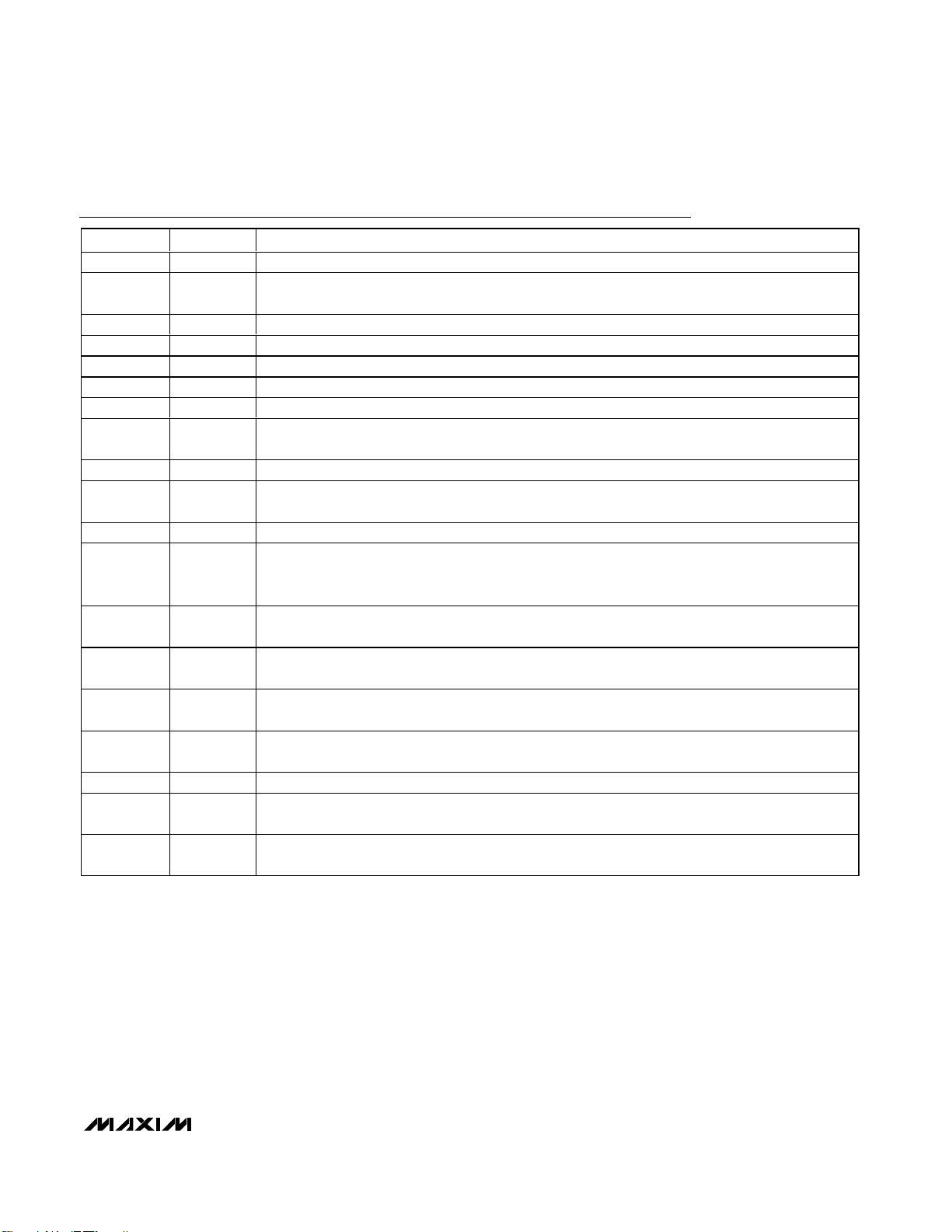
Pin Description
PIN NAME DESCRIPTION
1 DEGEN LNA Degeneration. Connect a 1nH to 3nH inductor from DEGEN to ground.
2R
LNA
LNA Bias. Connect an 18kΩ to 24kΩ resistor from R
LNA
to ground. Adjust R
LNA
to adjust the linearity
of the input LNA in the HGHL mode.
3 GND Ground. Connect to PC board ground plane using low-inductance vias.
4 LNAIN RF Input. Requires a DC-blocking capacitor, which can be used as part of the matching network.
5 MODE0 Logic Input. See Table 1.
6 MODE1 Logic Input. See Table 1.
7 MODE2 Logic Input. See Table 1.
8, 11, 14, 18,
24, 25, 27
N.C. No Connection. These pins are internally unconnected. Connect to the PC board ground plane.
9 LO/2 Logic Input. Drive low to disable the LO/2. Drive high to enable the LO/2.
10 LO_IN
LO Input. Internally matched to 50Ω. Requires an external DC-blocking capacitor. The LO input
frequency can be internally divided by two prior to application to the mixer by driving LO/2 high.
12, 23 I.C. Internally Connected. Leave these pins unconnected for proper operation.
13 LO_OUT
LO Buffer Output. Internally matched to 50Ω. Does not require a DC-blocking capacitor. The output
frequency of the buffer is equal to the LO frequency divided by two when LO/2 is high, or the LO
frequency when LO/2 is low.
15, 16, 26
V
CC
Power Supply. Bypass pins 16 and 26 to the PC board ground with a capacitor placed as close to the
pin as possible. Do not share capacitor ground vias with other ground connections.
17 BUFFEN
LO Output Buffer Enable. Drive high to enable the LO output buffer. Drive low to disable the LO
output buffer.
19, 20
IF_CDMA-,
Differential IF Output Port. Requires pullup inductors to VCC, which can be used as part of the
matching network.
21 R
BIAS
Bias Resistor Connection. Connect an 18kΩ to 24kΩ resistor from R
BIAS
to ground. Adjust R
BIAS
to
adjust the linearity of the input LNA in all modes except HGHL and the mixer in all modes.
22 MIXIN Mixer Input. Requires an external matching network
28 LNAOUT
LNA Output. Requires an external pullup inductor to V
CC
and a DC-blocking capacitor, both of which
can be used as part of the matching network.
—EP
Exposed-Paddle Ground Connection. Solder the exposed paddle (EP) evenly to the board’s ground
plane for proper operation.
IF_CDMA+
Page 6
MAX2335
Detailed Description
Low-Noise Amplifiers (LNAs)
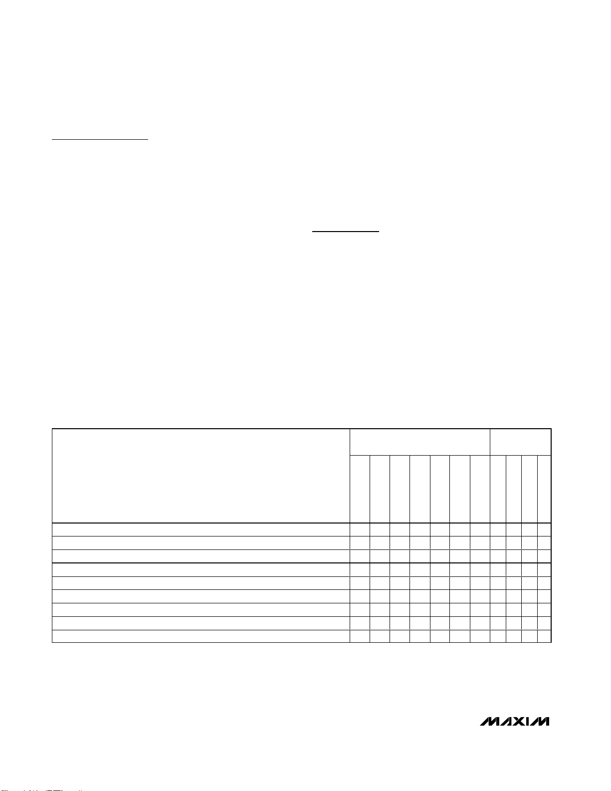
The MAX2335’s LNA gain and linearity characteristics
can be adjusted using the MODE[2:0] inputs. See
Table 1 for the pin settings for various operating
modes. Use high-gain, high-linearity mode (HGHL)
when extra-high linearity is required for cross-modulation suppression in the presence of strong interfering
signals (e.g., when the system transmitter is on). Use
high-gain, low-linearity mode (HGLL) when the transmitter is off and cross-modulation is not a concern, and
use low-gain mode (LG) when receiving large signals.
R
LNA
can be adjusted to vary the current and linearity
of the HGHL LNA. R
BIAS
adjusts the current and the lin-
earity of the HGLL and LG LNA.
Downconverter
The mixer requires a DC-blocking capacitor at the input
and pullup inductors at the output. The DC-blocking
capacitors and pullup inductors can be designed to be
part of the matching circuits. See Table 1 for the MODE
settings for various operating modes.
LO Output Buffer
The LO output buffer is internally matched to 50Ω and
includes a DC-blocking capacitor. Enable the buffer by
driving the BUFFEN input high; disable the buffer by
driving the BUFFEN input low. The frequency of the
buffer output is equal to the LO frequency if the LO/2
input is driven low, or equal to the LO frequency divided by two if LO/2 is driven high.
Applications Information
Cascaded LNA/Mixer Performance
The LNA and mixer design optimizes cascaded performance in all gain and linearity modes. In HGHL mode,
both the LNA and mixer have a low noise figure, high
gain, and high linearity. The LNA has high gain to minimize the noise contribution of the mixer, thus increasing
the receiver’s sensitivity, and the LNA has high linearity
for cross-modulation suppression. The HGLL mode is
used when the transmitter is off and cross-modulation
is not a concern. In LG mode, the received signal is
strong enough that linearity is the primary concern. The
LNA gain is reduced to achieve higher system linearity.
S-Parameters
The S-parameters in Tables 2, 3, and 4 can be used to
design the RF matching circuits.
450MHz CDMA/OFDM LNA/Mixer
6 _______________________________________________________________________________________
FUNCTION
CONTROL
PINS
MODES
LO/1
LO/2
HGHL LNA
HGLL LNA
LG LNA
HGHL MIXER
HGLL MIXER
MODE2
MODE1
MODE0
LO/2
HGHL (LO Frequency Divided by Two)
1
HGLL (LO Frequency Divided by Two)
1
LG (LO Frequency Divided by Two)
1
HGHL (LO Frequency Undivided)
0
HGLL (LO Frequency Undivided)
0
LG (LO Frequency Undivided)
0
Shutdown Mode
X
Undefined
X
Undefined
X
Table 1. Operating Modes
✓✓ ✓ 111
✓✓ ✓101
✓✓✓011
✓✓ ✓111
✓✓✓101
✓✓✓011
000
1X0
X10
Page 7
MAX2335
450MHz CDMA/OFDM LNA/Mixer
_______________________________________________________________________________________ 7
FREQUENCY
(MHz)
S11 (dB)
∠S11
S21 (dB)
∠S21
S12 (dB)
∠S12
S22 (dB)
∠S22
( D EG R EES)
50 -0.693 -20.000 22.265 2.173
-39.133 -0.607 55.183
100 -1.302 -38.600 21.655 -41.256
-83.956 -0.532 10.563
150 -1.957 -54.244 20.037 -68.340
-107.964 -0.819 -11.252
200 -2.407 -68.840 18.300 -89.560
-124.383 -1.051 -26.637
250 -2.656 -82.550 16.860 -105.680
-136.021 -1.250 -39.640
300 -2.813 -97.830 15.354 -120.500
-147.784 -1.420 -51.424
350 -2.959 -112.274 14.262 -133.400
-161.620 -1.492 -63.020
400 -2.953 -127.226 12.926 -144.921
-172.633 -1.590 -73.860
410 -2.944 -130.500 12.710 -146.900
-174.766 -1.630 -76.200
420 -2.914 -133.724 12.530 -149.125
-177.340 -1.628 -78.540
430 -2.876 -136.800 12.439 -151.380
-179.138 -1.634 -80.612
440 -2.878 -139.320 12.220 -153.900
177.020 -1.650 -82.870
450 -2.884 -142.833 12.000 -155.650
176.320 -1.665 -84.900
460 -2.850 -145.863 11.820 -158.324
173.850 -1.667 -87.422
470 -2.828 -149.000 11.550 -160.300
171.027 -1.697 -89.183
480 -2.828 -159.962 11.343 -161.928
169.065 -1.711 -91.480
490 -2.811 -155.360 11.150 -163.540
167.483 -1.720 -93.335
500 -2.763 -158.386 11.060 -165.000
164.144 -1.718 -95.970
550 -2.628 -174.012 10.298 -174.600
152.660 -1.756 -107.020
600 -2.444 169.970 9.810 178.350
139.530 -1.770 -117.930
650 -2.230 153.600 9.255 170.400
128.572 -1.778 -129.730
700 -1.989 137.420 9.200 162.304
117.290 -1.776 -141.100
750 -1.733 121.170 9.164 154.522
106.200 -1.828 -152.555
800 -1.464 104.500 9.470 146.813
94.020 -1.778 -164.610
850 -1.236 87.855 9.690 135.700
83.711 -1.810 -176.805
900 -0.978 73.488 10.432 127.430
70.714 -1.860 170.521
950 -0.889 53.876 10.613 112.950
59.976 -1.887 158.326
1000 -0.858 36.186 11.417 101.010
45.167 -2.033 145.377
Table 2. MAX2335 LNA S-Parameters in HGHL Mode
( D EG R EES)
( D EG R EES)
( D EG R EES)
-45.196
-37.836
-33.411
-31.340
-29.466
-28.422
-26.605
-25.600
-25.519
-25.062
-24.960
-24.780
-24.500
-24.465
-24.239
-24.180
-23.736
-23.568
-22.850
-21.890
-21.400
-20.375
-20.230
-19.626
-19.430
-18.654
-18.512
-17.839
Page 8

MAX2335
Power-Supply Layout
To minimize coupling between different sections of the
IC, use a star configuration, which has a large decoupling capacitor at a central VCCnode. The VCCtraces
branch out from this node, each going to a separate
VCCpin of the MAX2335. At the end of each trace is a
bypass capacitor with impedance to ground less than
1Ω at the frequency of interest. This arrangement provides local decoupling at each VCCpin. Use at least
one via per bypass capacitor for a low-inductance
ground connection. Also, connect the exposed paddle
to the PC board GND with multiple vias to provide the
lowest inductance ground connection possible.
Matching Network Layout
The layout of a matching network can be very sensitive
to parasitic circuit elements. To minimize parasitic
inductance, keep all traces short and place components as close to the IC as possible.
Use high-Q components for the LNA input-matching
network to achieve the lowest possible noise figure.
Keep the distance between the differential signal lines
at the mixer outputs constant and make both lines of
equal length to ensure signal balance.
Chip Information
PROCESS: SiGe
450MHz CDMA/OFDM LNA/Mixer
8 _______________________________________________________________________________________
Table 3. MAX2335 Mixer Input Impedance
in HGHL Mode
Table 4. MAX2335 Mixer Output
Impedance (Shunt RC) in HGHL Mode
FREQUENCY (MHz) S11 (dB)
∠S11
(DEGREES)
400 -1.2 77.23
410 -1.229 74.52
420 -1.247 71.7
430 -1.24 69.124
440 -1.24 66.47
450 -1.25 63.97
460 -1.28 61.455
470 -1.32 58.68
480 -1.33 55.87
490 -1.35 53.565
500 -1.35 50.87
EQUIVALENT
IF FREQUENCY
(MHz)
80 17.7 1.21
100 16.961 1.21
120 15.79 1.21
140 14.616 1.21
160 13.49 1.21
190 11.87 1.21
SHUNT
RESISTANCE
(kΩ)
EQUIVALENT
SHUNT
CAPACITANCE
(pF)
Page 9

MAX2335
450MHz CDMA/OFDM LNA/Mixer
_______________________________________________________________________________________ 9
Typical Application Circuit
V
CC
465MHz
BANDPASS
FILTER
LO INPUT
CHARGE-
PUMP OUTPUT
PLL INPUT
V
CC
47nH
IF OUT+
IF OUT-
0.01µF
6.8pF
6.8pF
100pF
3.9pF
6800pF
V
CC
V
CC
470Ω
1kΩ
18kΩ
20Ω
18nH
24kΩ
1nH
22nH
270nH
270nH
100pF
RFPLL
19.2MHz
TCXO
REFERENCE
INPUT
100pF
DUPLEXER
0.01µF
1GHz
VCO
MAX2335
MAX2370
÷2
5
6
4
3
17
16
18
R
LNA
LNAIN
MODEO
MODE1
MODE2
MODEO
MODE1
MODE2
19
DEGEN
IF_CDMA+
N.C.
BUFFEN
EP
R
BIAS
V
CC
V
CC
89
N.C.
11 12 13 14
2728 26 24 23 22
V
CC
N.C.
LO_IN
N.C.
I.C.
LO_OUT
GND
IF_CDMA-
10
25
7
15
LNAOUT
N.C.
N.C.
2
20
LO/2
I.C.
1
21
N.C.
MIXIN
+
V
CC
V
CC
1000pF100pF
100pF
22µF
LO BUFFER
ENABLE
PA
Page 10

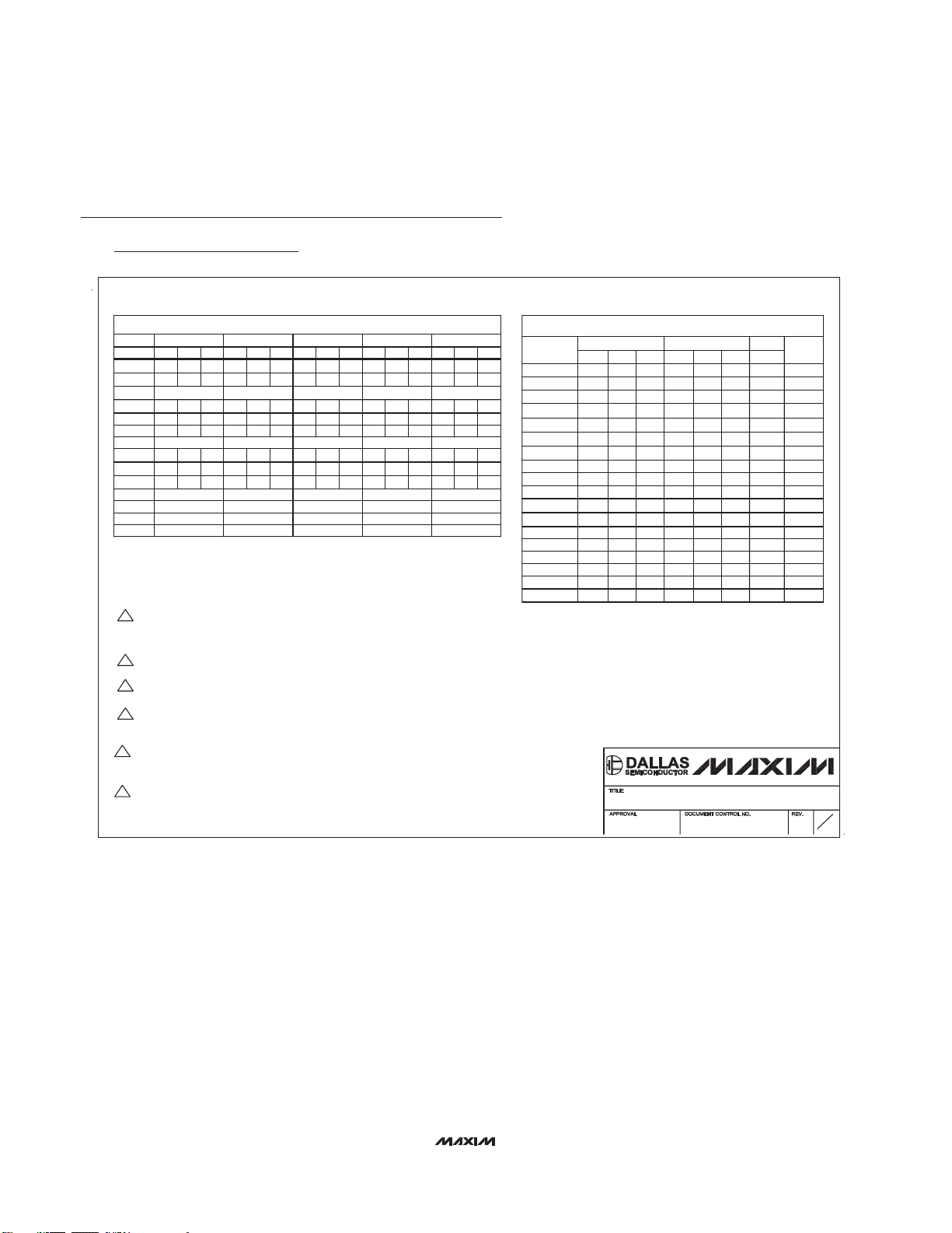
Package Information
(The package drawing(s) in this data sheet may not reflect the most current specifications. For the latest package outline information
go to www.maxim-ic.com/packages
.)
QFN THIN.EPS
D2
(ND-1) X e
e
D
C
PIN # 1
I.D.
(NE-1) X e
E/2
E
0.08 C
0.10 C
A
A1
A3
DETAIL A
E2/2
E2
0.10 M C A B
PIN # 1 I.D.
b
0.35x45°
D/2
D2/2
L
C
L
C
e e
L
CC
L
k
L
L
DETAIL B
L
L1
e
AAAAA
MARKING
I
1
2
21-0140
PACKAGE OUTLINE,
16, 20, 28, 32, 40L THIN QFN, 5x5x0.8mm
-DRAWING NOT TO SCALE-
L
e/2
MAX2335
450MHz CDMA/OFDM LNA/Mixer
10 ______________________________________________________________________________________
Page 11
MAX2335
450MHz CDMA/OFDM LNA/Mixer
Maxim cannot assume responsibility for use of any circuitry other than circuitry entirely embodied in a Maxim product. No circuit patent licenses are
implied. Maxim reserves the right to change the circuitry and specifications without notice at any time.
Maxim Integrated Products, 120 San Gabriel Drive, Sunnyvale, CA 94086 408-737-7600 ____________________ 11
© 2005 Maxim Integrated Products Printed USA is a registered trademark of Maxim Integrated Products, Inc.
COMMON DIMENSIONS
MAX.
EXPOSED PAD VARIATIONS
D2
NOM.MIN.
MIN.
E2
NOM. MAX.
NE
ND
PKG.
CODES
1. DIMENSIONING & TOLERANCING CONFORM TO ASME Y14.5M-1994.
2. ALL DIMENSIONS ARE IN MILLIMETERS. ANGLES ARE IN DEGREES.
3. N IS THE TOTAL NUMBER OF TERMINALS.
4. THE TERMINAL #1 IDENTIFIER AND TERMINAL NUMBERING CONVENTION SHALL
CONFORM TO JESD 95-1 SPP-012. DETAILS OF TERMINAL #1 IDENTIFIER ARE
OPTIONAL, BUT MUST BE LOCATED WITHIN THE ZONE INDICATED. THE TERMINAL #1
IDENTIFIER MAY BE EITHER A MOLD OR MARKED FEATURE.
5. DIMENSION b APPLIES TO METALLIZED TERMINAL AND IS MEASURED BETWEEN
0.25 mm AND 0.30 mm FROM TERMINAL TIP.
6. ND AND NE REFER TO THE NUMBER OF TERMINALS ON EACH D AND E SIDE RESPECTIVELY.
7. DEPOPULATION IS POSSIBLE IN A SYMMETRICAL FASHION.
8. COPLANARITY APPLIES TO THE EXPOSED HEAT SINK SLUG AS WELL AS THE TERMINALS.
9. DRAWING CONFORMS TO JEDEC MO220, EXCEPT EXPOSED PAD DIMENSION FOR
T2855-3 AND T2855-6.
NOTES:
SYMBOL
PKG.
N
L1
e
E
D
b
A3
A
A1
k
10. WARPAGE SHALL NOT EXCEED 0.10 mm.
JEDEC
0.70 0.800.75
4.90
4.90
0.25
0.250--
4
WHHB
4
16
0.350.30
5.10
5.105.00
0.80 BSC.
5.00
0.05
0.20 REF.
0.02
MIN. MAX.NOM.
16L 5x5
L
0.30 0.500.40
---
---
WHHC
20
5
5
5.00
5.00
0.30
0.55
0.65 BSC.
0.45
0.25
4.90
4.90
0.25
0.65
--
5.10
5.10
0.35
20L 5x5
0.20 REF.
0.75
0.02
NOM.
0
0.70
MIN.
0.05
0.80
MAX.
---
WHHD-1
28
7
7
5.00
5.00
0.25
0.55
0.50 BSC.
0.45
0.25
4.90
4.90
0.20
0.65
--
5.10
5.10
0.30
28L 5x5
0.20 REF.
0.75
0.02
NOM.
0
0.70
MIN.
0.05
0.80
MAX.
---
WHHD-2
32
8
8
5.00
5.00
0.40
0.50 BSC.
0.30
0.25
4.90
4.90
0.50
--
5.10
5.10
32L 5x5
0.20 REF.
0.75
0.02
NOM.
0
0.70
MIN.
0.05
0.80
MAX.
0.20 0.25 0.30
DOWN
BONDS
ALLOWED
YES3.103.00 3.203.103.00 3.20T2055-3
3.103.00 3.203.103.00 3.20
T2055-4
T2855-3 3.15 3.25 3.35 3.15 3.25 3.35
T2855-6
3.15 3.25 3.35 3.15 3.25 3.35
T2855-4 2.60 2.70 2.80 2.60 2.70 2.80
T2855-5 2.60 2.70 2.80 2.60 2.70 2.80
T2855-7 2.60 2.70
2.80
2.60 2.70 2.80
3.20
3.00 3.10T3255-3 3 .203.00 3.10
3.203.00 3.10T3255-4 3 .203.00 3.10
NO
NO
NO
NO
YES
YES
YES
YES
3.203.00T1655-3 3.10 3.00 3.10 3.20 NO
NO3.203.103.003.10T1655N-1 3.00 3.20
3.353.15T2055-5 3.25 3.15 3.25 3.35
YES
3.35
3.15
T2855N-1
3.25 3.15 3.25 3.35
NO
3.353.15T2855-8 3.25 3.15 3.25 3.35
YES
3.203.10T3255N-1 3.00
NO
3.203.103.00
L
0.40
0.40
**
**
**
**
**
**
**
**
**
**
**
**
**
**
SEE COMMON DIMENSIONS TABLE
±0.15
11. MARKING IS FOR PACKAGE ORIENTATION REFERENCE ONLY.
I
2
2
21-0140
PACKAGE OUTLINE,
16, 20, 28, 32, 40L THIN QFN, 5x5x0.8mm
-DRAWING NOT TO SCALE-
12. NUMBER OF LEADS SHOWN ARE FOR REFERENCE ONLY.
3.30T4055-1 3.20 3.40 3.20 3.30 3.40
**
YES
0.050 0.02
0.600.40 0.50
10
-----
0.30
40
10
0.40 0.50
5.10
4.90 5.00
0.25 0.35 0.45
0.40 BSC.
0.15
4.90
0.250.20
5.00 5.10
0.20 REF.
0.70
MIN.
0.75 0.80
NOM.
40L 5x5
MAX.
13. LEAD CENTERLINES TO BE AT TRUE POSITION AS DEFINED BY BASIC DIMENSION "e", ±0.05.
T1655-2
**
YES3.203.103.003.103.00 3.20
T3255-5 YES3.003.103.00
3.20
3.203.10
**
exceptions
Package Information (continued)
(The package drawing(s) in this data sheet may not reflect the most current specifications. For the latest package outline information
go to www.maxim-ic.com/packages
.)
 Loading...