

For free samples & the latest literature: http://www.maxim-ic.com, or phone 1-800-998-8800.
For small orders, phone 1-800-835-8769.
General Description
The MAX2310/MAX2312/MAX2314/MAX2316 are IF
receivers designed for dual-band, dual-mode, and single-mode N-CDMA and W-CDMA cellular phone systems. The signal path consists of a variable gain
amplifier (VGA) and I/Q demodulator. The devices feature guaranteed +2.7V operation, a dynamic range of
over 110dB, and high input IP3 (-33dBm at 35dB gain,
1.7dBm at -35dB).
Unlike similar devices, the MAX2310 family of receivers
includes dual oscillators and synthesizers to form a
self-contained IF subsystem. The synthesizer’s reference and RF dividers are fully programmable through a
3-wire serial bus, enabling dual-band system architectures using any common reference and IF frequency.
The differential baseband outputs have enough bandwidth to suit both N-CDMA and W-CDMA systems, and
offer saturated output levels of 2.7Vp-p at a low +2.75V
supply voltage. Including the low-noise voltage-controlled oscillator (VCO) and synthesizer, the MAX2310
draws only 26mA from a +2.75V supply in CDMA (differential IF) mode.
The MAX2310/MAX2312/MAX2314/MAX2316 are available in 28-pin QSOP packages.
Applications
Single/Dual/Triple-Mode CDMA Handsets
Globalstar Dual-Mode Handsets
Wireless Data Links
Tetra Direct-Conversion Receivers
Wireless Local Loop (WLL)
Features
♦ Complete IF Subsystem Includes VCO and
Synthesizer
♦ Supports Dual-Band, Triple-Mode Operation
♦ VGA with >110dB Gain Control
♦ Quadrature Demodulator
♦ High Output Level (2.7V)
♦ Programmable Charge-Pump Current
♦ Supports Any IF Frequency Between 40MHz and
300MHz
♦ 3-Wire Programmable Interface
♦ Low Supply Voltage (+2.7V)
MAX2310/MAX2312/MAX2314/MAX2316
CDMA IF VGAs and I/Q Demodulators
with VCO and Synthesizer
________________________________________________________________
Maxim Integrated Products
1
19-1507; Rev 0a; 8/99
PART
MAX2310EEI
MAX2312EEI
-40°C to +85°C
-40°C to +85°C
TEMP. RANGE PIN-PACKAGE
28 QSOP
28 QSOP
EVALUATION KIT MANUAL
FOLLOWS DATA SHEET
Pin Configurations appear at end of data sheet.
Block Diagram appears at end of data sheet.
Ordering Information
Selector Guide
MAX2314EEI
MAX2316EEI
-40°C to +85°C
-40°C to +85°C 28 QSOP
28 QSOP
Single Band, Dual Mode
AMPS,
Cellular CDMA
MAX2314
Single Band, Single ModePCS CDMA
Dual Band, Triple Mode
AMPS,
Cellular CDMA,
PCS CDMA
MAX2310
MAX2312
DESCRIPTIONMODEPART
Single Band, Single Mode or
Single Band, Dual Mode with
External Discriminator
Cellular CDMAMAX2316 40MHz to 150MHz
40MHz to 150MHz
67MHz to 300MHz
40MHz to 300MHz
INPUT RANGE
I
CC
MAX2310/MAX2312/MAX2314/MAX2316
CDMA IF VGAs and I/Q Demodulators
with VCO and Synthesizer
2 _______________________________________________________________________________________
ABSOLUTE MAXIMUM RATINGS
DC ELECTRICAL CHARACTERISTICS
(VCC= +2.7V to +5.5V, MODE = DIVSEL = SHDN = STBY = BUFEN = high, differential output load = 10kΩ, TA= -40°C to +85°C,
registers set to default power-up settings. Typical values are at V
CC
= +2.75V and TA= +25°C, unless otherwise noted.)
Stresses beyond those listed under “Absolute Maximum Ratings” may cause permanent damage to the device. These are stress ratings only, and functional
operation of the device at these or any other conditions beyond those indicated in the operational sections of the specifications is not implied. Exposure to
absolute maximum rating conditions for extended periods may affect device reliability.
VCCto GND..............................................................-0.3V, +6.0V
SHDN to GND.............................................-0.3V to (V
CC
+ 0.3V)
STBY, BUFEN, MODE, EN, DATA,
CLK, DIVSEL ...........................................-0.3V to (V
CC
+ 0.3V)
VGC to GND...............-0.3V, the lesser of +4.2V or (V
CC
+ 0.3V)
AC Signals TankH ±, TankL ±,
REF, FM ±, CDMA ± .................................................1.0V peak
Digital Input Current SHDN, MODE, DIVSEL,
BUFEN, DATA, CLK, EN, STBY .....................................±10mA
Continuous Power Dissipation (T
A
= +70°C)
28-pin QSOP (derate 10mW/°C above T
A
= +70°C) ....800mW
Operating Temperature Range ...........................-40°C to +85°C
Junction Temperature......................................................+150°C
Storage Temperature Range .............................-65°C to +160°C
Lead Temperature (soldering, 10sec) .............................+300°C
VCC= 2.75V
CDMA mode
I+ to I- and Q+ to Q-, PLL locked
50kΩ load
50kΩ load
SHDN = low
0.5V < V
VGC
< 2.3V
Addition for LO out (BUFEN = low)
CONDITIONS
VVCC- 1.4Common-Mode Output Voltage
mV-20 ±1.5 +20DC Offset Voltage
V0.5Lock Indicator Low (unlocked)
V2.0Lock Indicator High (locked)
µA1
VGC Control Input Current
During Shutdown
µA-5 5VGC Control Input Current
µA2I
IL
Logic Low Input Current
41.5
25.9 37.5
µA2I
IH
Logic High Input Current
V0.5Logic Low
V2.0Logic High
mA3 5.8I
CC
Register Shutdown Current
3.5
UNITSMIN TYP MAXSYMBOLPARAMETER
TA= +25°C
TA= -40°C to +85°C
I
CC
Supply Current (Note 1) mA
TA= +25°C
TA= -40°C to +85°C
FM IQ mode
40.6
25.4 36.7
TA= +25°C
TA= -40°C to +85°C
FM I mode
39.5
24.7 35.7
TA= +25°C
TA= -40°C to +85°C
STANDBY (VCO_H)
20.7
12.3 18.8
TA= +25°C
TA= -40°C to +85°C
STANDBY (VCO_L)
20.3
11.5 18.4
SHDN = low
µA1.5 10I
CC
Shutdown Current
MAX2310/MAX2312/MAX2314/MAX2316
CDMA IF VGAs and I/Q Demodulators
with VCO and Synthesizer
_______________________________________________________________________________________ 3
AC ELECTRICAL CHARACTERISTICS
(MAX2310/MAX2314 or MAX2312/MAX2316 EV kit, VCC= +2.75V, registers set to default power-up states, f
IN
= 210.88MHz for
CDMA, f
IN
= 85.88MHz for FM, f
REF
= 19.68MHz, synthesizer locked with passive 2nd-order lead-lag loop filter, SHDN = high, VGC
set for +35dB voltage gain, differential output load = 10kΩ, all power levels referred to 50Ω, T
A
= +25°C, unless otherwise noted.)
(Note 2)
(Note 2)
Gain = +35dB
(Note 5)
Gain = -35dB
Gain = +35dB
Gain = -35dB
Gain = -35dB (Note 3)
Gain = +35dB (Note 4)
CONDITIONS
dBm
-31
IIP3Input Third-Order Intercept
-6.0
dB
6.36
NFDSB Noise Figure
62.9
dB56 61.3A
V
Maximum Voltage Gain
dB-54.8 -49A
V
Minimum Voltage Gain
Vp-p0.2V
REF
Frequency Reference Signal
Level
MHz39f
REF
MHz40 300f
IN
Input Frequency
Reference Frequency
dBm
-49
Input 0.25dB Desensitization
-14.8
dBm
-44 -38.3
P
1dB
Input 1dB Compression
-9 -6.4
1.7
dBm
-33.2
IIP3Input Third-Order Intercept
UNITSMIN TYP MAXSYMBOLPARAMETER
(Notes 6, 8) dBm
-44 -38.4
P
1dB
Input 1dB Compression
-20 -16.2
dB58.5 63.4A
V
Maximum Voltage Gain
dB-50.2 -47.4A
V
Minimum Voltage Gain
MHz4.2
Normalized to +25°C
Baseband 0.5dB Bandwidth
Differential
TA= T
MIN
to T
MAX
Vp-p2.7V
SAT
Saturated Output Level
mVp-p
dB±2.5
Maximum Gain Variation
Over Temperature
1LO to Baseband Leakage
dB+30 +35Quadrature Suppression
RL= 50Ω, BUFEN = low
(Note 2)
dBm-13.7P
LO
LOOUT Output Power
MHz
135 600f
VCO_H
VCO Tune Range
80 300f
VCO_L
SIGNAL PATH, CDMA MODE
SIGNAL PATH, FM_IQ MODE
SIGNAL PATH, CDMA and FM_IQ MODE
PHASE-LOCKED LOOP
Gain = +35dB
VGC= 0.5V (Note 6)
Gain = -35dB
Gain = -35dB
VGC= 0.5V (Note 6)
Gain = -35dB
Gain = +35dB
(Note 7)
Gain = +35dB
VGC= 2.3V (Note 6)
VGC= 2.3V (Note 6)
MAX2310/MAX2312/MAX2314/MAX2316
CDMA IF VGAs and I/Q Demodulators
with VCO and Synthesizer
4 _______________________________________________________________________________________
AC ELECTRICAL CHARACTERISTICS (continued)
(MAX2310/MAX2314 or MAX2312/MAX2316 EV kit, VCC= +2.75V, registers set to default power-up states, f
IN
= 210.88MHz for
CDMA, f
IN
= 85.88MHz for FM, f
REF
= 19.68MHz, synthesizer locked with passive 2nd-order lead-lag loop filter, SHDN = high, VGC
set for +35dB voltage gain, differential output load = 10kΩ, all power levels referred to 50Ω, T
A
= +25°C, unless otherwise noted.)
120kHz offset
30kHz offset
-119
12.5kHz offset
1kHz offset
(Note 6)
(Note 6)
CONDITIONS
-110
30kHz offset
12.5kHz offset
-105
1kHz offset
900kHz offset
-91
-100
-72
dBc-50Base Band Spurious due to PLL
-64
dBc/Hz
-125
LOOUT at 85MHz,
VCO_L Enabled (Note 9)
900kHz offset
kHz1500
Maximum Phase Detector
Comparison Frequency
kHz20
Minimum Phase Detector
Comparison Frequency
2047R1, R2REF Maximum Divide Ratio
2R1, R2REF Minimum Divide Ratio
16383M1, M2VCO Maximum Divide Ratio
dBc/Hz
-125
256M1, M2VCO Minimum Divide Ratio
UNITSMIN TYP MAXSYMBOLPARAMETER
120kHz offset
LOOUT at 210MHz,
VCO_H Enabled (Note 9)
Locked, CPX = 00
Acquisition, CPX = XX, TC = 1
105 150 190
-115
1480 2100 2650
Charge-Pump Source/Sink
Current
Note 1: FM_IQ and FM_I modes are not available on MAX2312 and MAX2316.
Note 2: Recommended operating frequency range.
Note 3: f
1
= 210.88MHz, f2= 210.89MHz, P
f1
= P
f2
= -15dBm.
Note 4: f
1
= 210.88MHz, f2= 210.89MHz, P
f1
= Pf2= -50dBm.
Note 5: Small-signal gain at 200kHz below the LO frequency will be reduced by less than 0.25dB when an interfering signal at
1.25MHz below the LO frequency is applied at the specified level.
Note 6: Guaranteed by design and characterization.
Note 7: f
1
= 85.88MHz, f2= 85.98MHz, P
f1
= Pf2= -15dBm.
Note 8: f
1
= 85.88MHz, f2= 85.98MHz, P
f1
= Pf2= -50dBm.
Note 9: Measured at LOOUT with BD = 0 (÷2 selected).
Locked, CPX = 10
Locked, CPX = 01
210 300 380
150 210 265
Locked, all values of CPX,
0.5V < VCP< V
CC
- 0.5V
Locked, CPX = 11
%0.2 10
Charge-Pump Source/Sink
Matching
µA
300 425 530
TURBO LOCK
MAX2310/MAX2312/MAX2314/MAX2316
CDMA IF VGAs and I/Q Demodulators
with VCO and Synthesizer
_______________________________________________________________________________________
5
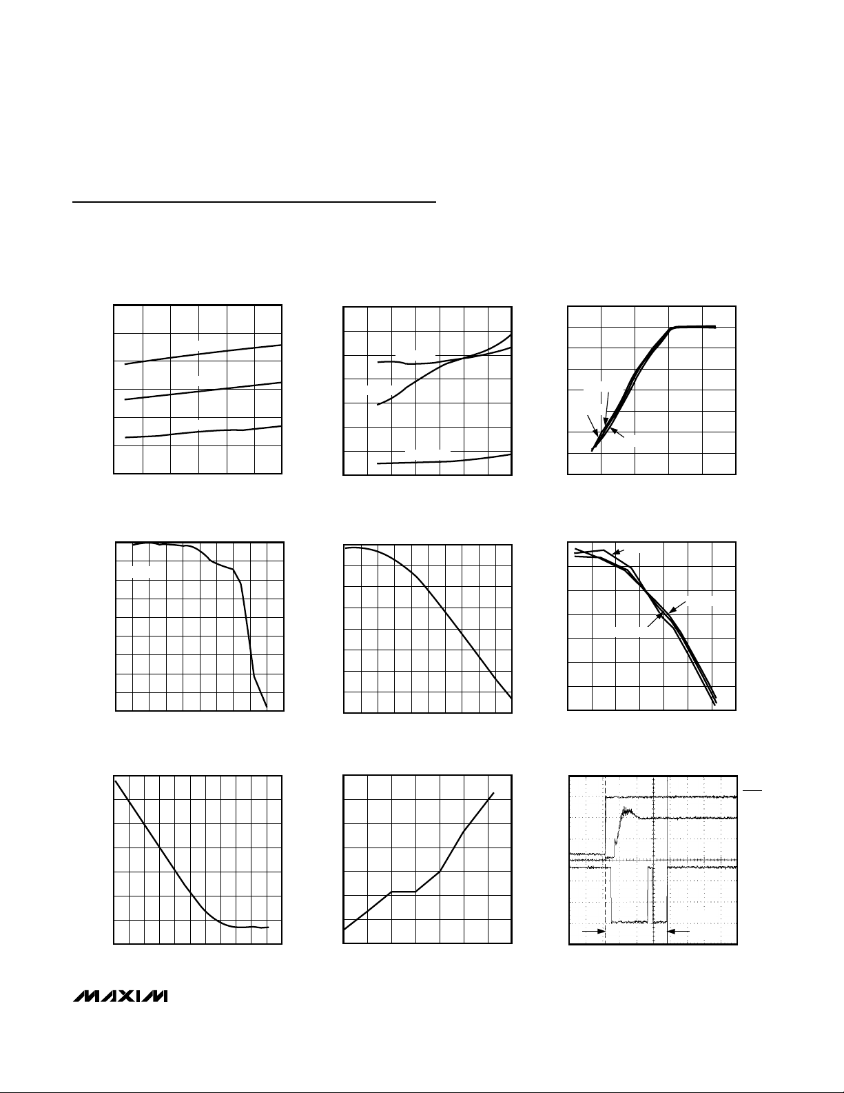
Typical Operating Characteristics
(MAX2310/MAX2314 or MAX2312/MAX2316 EV kit, VCC= +2.75V, registers set to default power-up states, fIN= 210.88MHz for
CDMA, f
IN
= 85.88MHz for FM, f
REF
= 19.68MHz, synthesizer locked with passive 2nd-order lead-lag loop filter, SHDN = high, VGC
set for +35dB voltage gain, differential output load = 10kΩ, all power levels referred to 50Ω, T
A
= +25°C, unless otherwise noted.)
SUPPLY CURRENT (mA)
GAIN (dB)
RECEIVE SUPPLY CURRENT
vs. SUPPLY VOLTAGE
35.00
32.50
30.00
27.50
25.00
22.50
20.00
2.5 3.5 4.03.0 4.5 5.0 5.5
TA = +85°C
TA = +25°C
TA = -40°C
SUPPLY VOLTAGE (V)
GAIN vs. INPUT FREQUENCY
60
55
VGC = 2.5V
50
45
40
35
30
25
20
15
0 100 200 300 400 500
FREQUENCY (MHz)
RECEIVE SHUTDOWN CURRENT vs.
TA = +25°C
GAIN vs. V
TA = +85°C
VGC (V)
GC
0.014
0.012
MAX2310 toc01
0.010
0.008
0.006
0.004
SHUTDOWN CURRENT (mA)
0.002
0
2.0 3.0 3.52.5 4.0 4.5 5.0 5.5
SUPPLY VOLTAGE
TA = +25°C
SUPPLY VOLTAGE (V)
TA = +85°C
TA = -40°C
MAX2310 toc02
80
60
40
20
0
GAIN (dB)
TA = -40°C
-20
-40
-60
-80
0.5 1.0 1.5 2.0 2.5 3.0
THIRD-ORDER INPUT
INTERCEPT vs. GAIN
TA = -40°C
TA = +85°C
TA = +25°C
GAIN (dB)
60.0
59.5
MAX2310 toc04
59.0
58.5
58.0
57.5
RELATIVE GAIN (dB)
57.0
56.5
56.0
GAIN vs. BASEBAND FREQUENCY
0 468102 1214161820
FREQUENCY (MHz)
MAX2310 toc05
10
0
-10
-20
IIP3 (dBm)
-30
-40
-50
-60
-60 -20 0-40 20 40 60 80
NAX2310 toc03
MAX2310 toc06
NOISE FIGURE vs. GAIN
70
60
50
40
NF (dB)
30
20
10
0
-40 -20 -10 0-30 10 20 5040 6030 70
GAIN (dB)
MAX2310 toc07
NOISE FIGURE vs. TEMPERATURE
7.4
7.2
7.0
6.8
NF (dB)
6.6
6.4
6.2
6.0
-40 0 20-20 40 60 80 100
TEMPERATURE (°C)
MAX2310 toc08
VOLTS (1V/div)
VCO VOLTAGE vs. TIME
LOCK TIME
1.83ms
TIME (500µs/div)
MAX2310 toc09
SHDN
VCO
VOLTAGE
LOCK
Pin Description
MAX2310/MAX2312/MAX2314/MAX2316
CDMA IF VGAs and I/Q Demodulators
with VCO and Synthesizer
6 _______________________________________________________________________________________
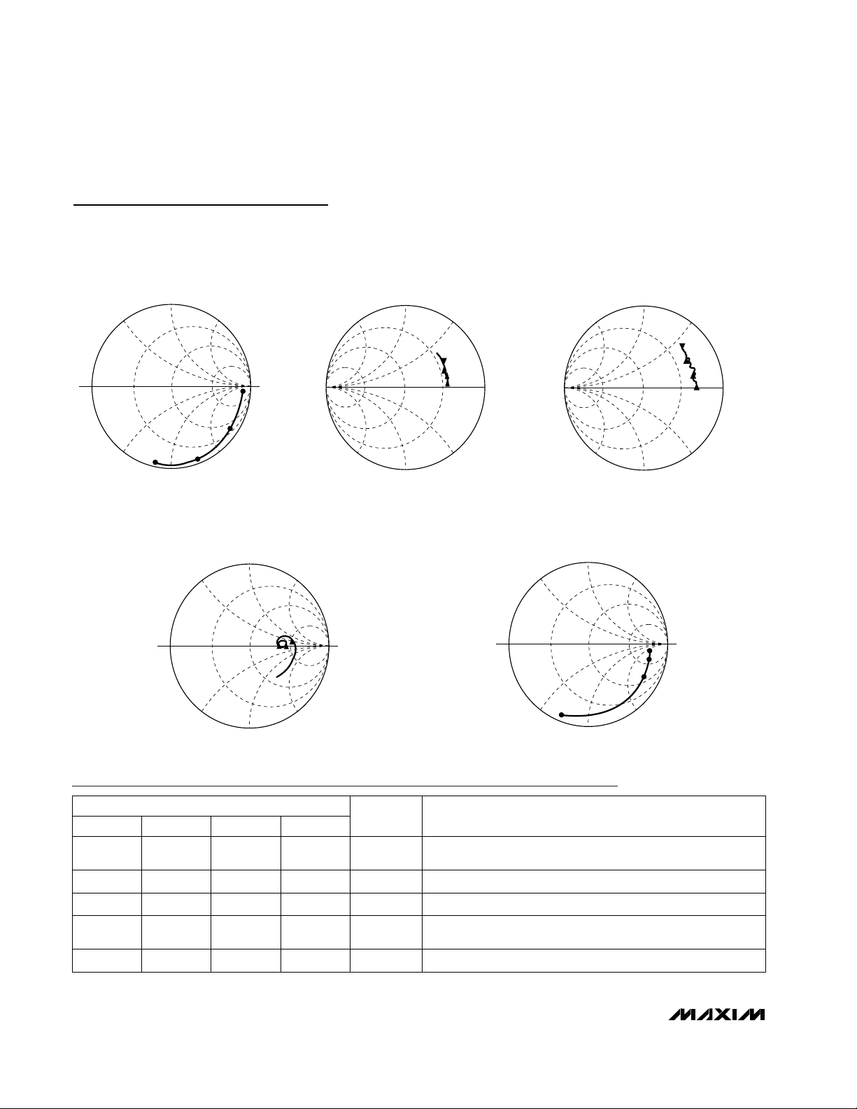
Typical Operating Characteristics (continued)
(MAX2310/MAX2314 or MAX2312/MAX2316 EV kit, VCC= +2.75V, registers set to default power-up states, fIN= 210.88MHz for
CDMA, f
IN
= 85.88MHz for FM, f
REF
= 19.68MHz, synthesizer locked with passive 2nd-order lead-lag loop filter, SHDN = high, VGC
set for +35dB voltage gain, differential output load = 10kΩ, all power levels referred to 50Ω, T
A
= +25°C, unless otherwise noted.)
LOOUT PORT
S22 vs. FREQUENCY
MAX2310 toc13
1: 108.63Ω (Re)
10.266Ω (1m)
40MHz
2: 134.99Ω (Re)
13.71Ω (1m)
150MHz
3: 158.83Ω (Re)
39.58Ω (1m)
300MHz
CDMA PORT
S11 vs. FREQUENCY
MAX2310 toc14
1: 10MHz, 375Ω - j56Ω
2: 85MHz, 285Ω - j200Ω
3: 210MHz, 73Ω - j169Ω
4: 600MHz, 2.1Ω - j34Ω
1
4
2
3
MAX2316MAX2314
PIN
NAME
11, 8 BYP
Bypass Node. Must be capacitively decoupled (bypassed)
to analog ground.
11
22 CP_OUT Charge-Pump Output 22
33 GND Analog Ground Reference33
5, 64, 5
TANKL+,
TANKL-
Differential Tank Input for Low-Frequency Oscillator—4, 5
4— DIVSEL High selects M1/R1; low selects M2/R2.4—
MAX2312MAX2310
FUNCTION
FM PORT
S11 vs. FREQUENCY
TANKL PORT
1/S11 vs. FREQUENCY
TANKH PORT
1/S11 vs. FREQUENCY
MAX2310 toc10
4
3
2
1
2
3
4
1: 641 - j428 10MHz
2: 27 - j162 85MHz
3: 4 - j73 210MHz
4: 1.8 - j39 600MHz
1
1: -3.06ms + j349µs, 100MHz
2: -3.01ms + j853µs, 160MHz
3: -3.11ms + j1.45ms, 240MHz
4: -3.04ms + j1.85ms, 300MHz
MAX2310 toc11
4
3
2
1
1: 1.98ms + j437µs, 100MHz
2: 2.18ms + j853µs, 160MHz
3: 2.11ms +j 2.53ms, 420MHz
4: 2.17ms +j 3.71ms, 600MHz
MAX2310 toc12
MAX2310/MAX2312/MAX2314/MAX2316
CDMA IF VGAs and I/Q Demodulators
with VCO and Synthesizer
_______________________________________________________________________________________ 7
Pin Description (continued)
27, 28 27, 28
Bypass Node. Must be capacitively decoupled (bypassed) to
analog V
CC
.
BYP27, 28 27, 28
23, 24 23, 24 Differential CDMA Input. Active in CDMA mode.
CDMA-,
CDMA+
23, 24 23, 24
25 — Differential Positive Input. Active in FM mode.FM+25 —
22 22 VGA Gain Control Input. Control voltage range is 0.5V to 2.3V.VGC22 22
20 20 Data input of the 3-wire serial bus.DATA20 20
19 19 Enable Input. When low, input shift register is enabled.
EN
19 19
18 18 Clock input of the 3-wire serial busCLK18 18
16, 17 16, 17
Differential Quadrature-Phase Baseband Output. Disabled if
FM_I mode is selected.
QOUT-,
QOUT+
16, 17 16, 17
15 15
Lock Output—open-collector pin. Logic high indicates phaselocked condition.
LOCK15 15
13, 14 13, 14
Differential In-Phase Baseband Output, or FM signal output
FM_I mode is selected.
IOUT+,
IOUT-
13, 14 13, 14
12 12
Shutdown Input—active low. Low powers down entire device,
including registers and serial interface.
SHDN
12 12
11 11 Reference Frequency InputREF11 11
— 8
Internal VCO Output. Depending on setting of BD bit, LOOUT
is either the VCO frequency (twice the IF frequency) or onehalf the VCO frequency (equal to the IF frequency).
LOOUT— 8
6, 7 5, 6 Differential Tank Input for High-Frequency Oscillator
TANKH+,
TANKH-
— —
NAME FUNCTION
PIN
MAX2310 MAX2312 MAX2314 MAX2316
— 7 LO Buffer Amplifier—active low
BUFEN
— 7
— — No Connection. Must be left open-circuit.N.C.6, 7 —
8 —
Mode Select. High selects CDMA mode; low selects FM
mode.
MODE— —
10 10 Digital GroundGND10 10
9 9 +2.7V to +5.5V Supply for Digital Circuits
V
CC
9 9
21 21 2.7V to 5.5V Supply for Analog Circuits
V
CC
21 21
26 —
Differential Negative Input for FM signal. Bypass to GND for
single-ended operation.
FM-26 —
— 26
Standby Input—active low. Low powers down VGA and demodulator while keeping VCO, PLL, and serial bus on.
STBY
— 26
— 25 No Connection.N.C.— 25

MAX2310/MAX2312/MAX2314/MAX2316
CDMA IF VGAs and I/Q Demodulators
with VCO and Synthesizer
8 _______________________________________________________________________________________
_______________Detailed Description
MAX2310
The MAX2310 is intended for dual-band (PCS and cellular) and dual-mode code division multiple access
(CDMA) and FM applications (Figure 1). The device
includes an IF variable-gain amplifier, quadrature
demodulator, dual VCOs, and dual-frequency synthesizers (Figure 7). Dual VCOs are provided for applications using different IF frequencies for each mode or
band of operation. The analog FM output signal can be
configured for conversion to the I channel, or it may be
converted in quadrature to both the I and Q channels.
The MAX2310’s operation modes are described in
Table 1. These modes are set by programming the control register and setting logic levels on control pins. If
MODE is left floating, the internal register controls the
operation. If driven high or low, mode will override certain register bits, as shown in Table 1.
Figure 1. MAX2310 Typical Operating Circuit
0.033µF
10k
10k
10k
10k
10k
47pF
0.01µF
3.3nF
18pF
5pF
18pF
12pF
1.5pF
12pF
V
CC
68nH
18nH
47pF
BYP
CPOUT
GND
TANKL+
MAX2310
TANKL-
TANKH+
TANKH-
MODE
V
CC
GND
REF
SHDN
IOUT+
FM+
CDMA+
CDMA-
VGC
DATA
QOUT+
BYP
BYP
FM-
V
CLK
0.01µF
V
CC
0.1µF
0.01µF
FM
680Ω
47pF
CC
EN
3-WIRE
CDMA
V
CC
DAC
I
10k
IOUT-
QOUT-
LOCK
10k
47k
V
CC
Q

M
S
B
MAX2312/MAX2316
The MAX2312/MAX2316 quadrature demodulators are
simplified versions of the MAX2310 that can be used in
single-mode CDMA or dual mode using an external FM
discriminator (Figures 2a and 2b). The MAX2312 VCO
is optimized for the 67MHz to 300MHz IF frequency
range, while the MAX2316 VCO is optimized for the
40MHz to 150MHz IF frequency range.
Both devices include a buffered output for the VCO.
The buffered VCO output can be used to support systems implementing traditional limiting IF stages for FM
demodulation in dual-mode phones as well as for the
transmit LO in TDD systems. This buffered output can
be configured for the VCO frequency (twice the IF frequency) or one-half the VCO frequency (IF frequency).
The BUFEN pin enables this feature. A standby mode,
in which only the VCO and synthesizer are operational,
can be selected through the serial interface or the
STBY pin. The MAX2312/MAX2316s’ operational modes
are described in Table 2. These modes are set by programming the control register and/or setting logic levels on control pins. If the control pins (STBY, BUFEN,
DIVSEL) are left floating, the internal register controls
the operational mode. If driven high or low, the control
pins will override certain register bits, as shown in
Table 2.
MAX2310/MAX2312/MAX2314/MAX2316
CDMA IF VGAs and I/Q Demodulators
with VCO and Synthesizer
_______________________________________________________________________________________ 9
Table 1. MAX2310 Control Register States
MODE
SHDN
PINS
XL
Shutdown pin completely
powers down the chip
SHUTDOWN
ACTION
RESULT
OPERATIONAL
MODE
TEST_MODE
X
CP POL
TEST_EN
XX
TURBOCHARGE
DIVSEL
X
VCO_BYP
VCO_SEL
XX X
BUF_DIV
BUFEN
XX
FM_TYPE
IN_SEL
X
STBY
SHDN
ML
S CONTROL REGISTER S
BB
XX X
X XXH X
0 in shutdown register bit leaves
serial port active
SHUTDOWN X XX X XX X 0X X
X 0XH X
0 in standby register bit turns off
VGA and modulator only
STANDBY XX 10
0HH
Mode pin overrides VCO_SEL,
DIVSEL, and IN_SEL to high
CDMA X X XX X 1X 1
0FH
Floating mode pin returns control
to register
CDMA 1 1 XX 1 1X 1
0LH
Mode pin overrides VCO_SEL,
DIVSEL, and IN_SEL to low
FM_IQ X X XX X 10 1
0FH
Floating mode pin returns control
to register
FM_IQ XX 0 10 1
0LH
Mode pin overrides VCO_SEL,
DIVSEL, and IN_SEL to low
FM_I X X XX X 11 1
0F
H
L
Floating pins return control to
register
FM_I XX 0 11 1
Note: H = high, L = low, F = floating pin, X = don’t care, Blank = independent parameter, 1 = logic high, 0 = logic low.

MAX2310/MAX2312/MAX2314/MAX2316
CDMA IF VGAs and I/Q Demodulators
with VCO and Synthesizer
10 ______________________________________________________________________________________
Figure 2a. MAX2312 Typical Operating Circuit
47pF
10k
0.033µF
10k
3300pF
12pF
0.01µF
BYP
CPOUT
GND
DIVSEL
TANKH+
BYP
BYP
STBY
CDMA+
0.01µF
0.01µF
V
CC
V
CC
10k
1.5pF
12pF
V
CC
I
47pF
18nH
10k
MAX2312
TANKH-
BUFEN
LOOUT
V
CC
GND
REF
SHDN
IOUT+
IOUT-
CDMA-
VGC
V
DATA
CLK
QOUT+
QOUT-
LOCK
680Ω
47pF
CC
EN
3-WIRE
10k
47k
V
CC
CDMA
V
CC
DAC
Q

MAX2310/MAX2312/MAX2314/MAX2316
CDMA IF VGAs and I/Q Demodulators
with VCO and Synthesizer
______________________________________________________________________________________ 11
Figure 2b. MAX2316 Typical Operating Circuit
DISCRIMINATOR
LIMITER
0.033µF
455kHz
10k
10k
10k
47pF
0.01µF
3300pF
17pF
5pF
18pF
V
CC
I
68nH
47pF
BYP
CP_OUT
GND
DIVSEL
TANKL+
MAX2316
TANKL-
BUFEN
LOOUT
V
CC
GND
REF
SHDN
IOUT+
BYP
BYP
STBY
CDMA+
CDMA-
VGC
V
DATA
CLK
QOUT+
0.01µF
V
CC
0.01µF
V
CC
680Ω
47pF
CC
EN
3-WIRE
10k10k
CDMA
V
CC
DAC
Q
FM
IOUT-
QOUT-
LOCK
47k
V
CC

MSB
MAX2310/MAX2312/MAX2314/MAX2316
CDMA IF VGAs and I/Q Demodulators
with VCO and Synthesizer
12 ______________________________________________________________________________________
Table 2. MAX2312/MAX2316 Control Register States
Note: H = high, L = low, 1 = logic high, 0 = logic low, X = don’t care, blank = independent parameter.
1
1
1
1
0 1
X 1
X 0
X X
SHDN
STBY
1/
0
X0
LO BUFFER
ENABLE
If pin is floated, then
BUFEN register bit
controls buffer
H F
XX0
LO BUFFER
ENABLE
BUFEN pin controls the
LO buffer and overrides
the bit
H/
L
H
X
1/
0
0
DIVIDER
SELECT
If DIV_SEL pin is floated, then register bit
selects divider
HH F
XX0
DIVIDER
SELECT
DIV_SEL pin overrides
DIV_SEL register bit
HH
H/
L
X0STANDBY
0 in standby register bit
turns off VGA and modulator only
H
H/
L
H
X0STANDBY
0 in standby pin turns
off VGA and modulator
only
LH
XX XXX XXX XXSHUTDOWN
0 in shutdown register
bit leaves serial bus
active
XH X XX
XX X
IN_SEL
FM_TYPE
X
BUFEN
OPERATIONAL
MODE
ACTION
RESULT
BUF_DIV
X X
VCO_SEL
VCO_BYP
XX X
DIVSEL
TURBOCHARGE
X
TES_TEN
SHUTDOWN
Shutdown pin completely powers down
the chip
CP_POL
XL X X
TEST_MODE
PINS
STBY
X
BUFEN
SHDN
DIVSEL
ML
S CONTROL REGISTER S
BB

MAX2310/MAX2312/MAX2314/MAX2316
CDMA IF VGAs and I/Q Demodulators
with VCO and Synthesizer
______________________________________________________________________________________ 13
MAX2314
The MAX2314 supports CDMA cellular-band, dualmode operation. As with the MAX2310, the FM mode
can be configured for conversion to the I port or quadrature conversion to both the I and Q ports (Figure 3).
The MAX2314’s operational modes are described in
Table 3. These modes are set by programming the
control register and setting logic levels on control pins.
__________Applications Information
Variable-Gain Amplifier and Demodulator
The MAX2310 family provides a Variable-Gain Amplifier
(VGA) with exceptional gain range. The MAX2310/
MAX2314 support multimode applications with dual differential inputs, selectable with the IN_SEL (IS) control
bit. On the MAX2310 this function can be controlled
with the MODE pin, which overrides the IS control bit.
The VGA’s gain is controlled over a 110dB range with
Figure 3. MAX2314 Typical Operating Circuit
0.033µF
10k
10k
10k
47pF
0.01µF
3300pF
BYP
MAX2314
CP_OUT
18pF
5pF
18pF
V
CC
68nH
1000pF
47pF
GND
TANKL+
TANKL-
BYP
V
CC
GND
REF
SHDN
I_OUT+
FM+
CDMA+
CDMA-
VGC
DATA
Q_OUT+
BYP
BYP
FM-
V
CLK
0.01µF
V
CC
0.01µF
V
CC
0.01µF
FM
680Ω
47pF
CC
EN
3-WIRE
CDMA
V
CC
DAC
10k
I_OUT-
Q_OUT-
LOCK
10k
47k
V
CC
Q

M
S
B
MAX2310/MAX2312/MAX2314/MAX2316
CDMA IF VGAs and I/Q Demodulators
with VCO and Synthesizer
14 ______________________________________________________________________________________
the VGC pin. The output of the VGA drives the RF ports
of a quadrature demodulator. The MAX2310/MAX2314
provide two types of FM demodulation, controlled by
the FM_TYPE (FT) control bit. When FM_TYPE is “1,”
the signal is passed through both the I and Q signal
paths for subsequent lowpass filtering and A/D conversion at baseband. If FM_TYPE is “0,” the FM signal is
passed through the I mixer only.
Voltage-Controlled Oscillator,
Buffers, and Quadrature Generation
The LO signal for downconversion is provided by a
voltage-controlled oscillator (VCO) consisting of an onchip differential oscillator, and an off-chip high-Q resonant network. Figure 4 shows a simplified schematic of
the VCO oscillator. Multiband operation is supported by
the MAX2310 with dual VCOs. VCO_H and VCO_L are
selectable with the MODE pin or the VCO_SEL (VS)
control bit. They oscillate at twice the desired LO frequency. For applications requiring an external LO, the
VCOs can be bypassed with the VCO_BYP (VB) control
bit.
The MAX2312/MAX2316 buffer the output of the VCO
and provide this signal at the LOOUT pin. This signal is
enabled by the BUFEN (BE) control bit or by the
BUFEN control pin. The frequency of this signal is
selected by the BUF_DIV (BD) control bit, and can be
either the VCO frequency or half the VCO frequency.
Quadrature downconversion is realized by providing inphase (I) and quadrature-phase (Q) components of the
LO signal to the LO ports of the demodulator described
above. The quadrature LO signals are generated by
dividing the VCO output frequency using two latches.
The appropriate latch outputs provide I and Q signals
at the desired LO frequency.
Table 3. MAX2314 Control Register States
Note: H = high, L = low, 1 = logic high, 0 = logic low, X = don’t care, blank = independent parameter
STBY
OPERATIONAL
MODE
11 10X X0FM_I FM I operation 0H
10 10X X0FM_IQ FM IQ quadrature operation 0H
1X 11X X0CDMA CDMA operation 0H
0 1X X0STANDBY
0 in standby pin turns off VGA and
modulator only
0H
XX LXX XXX XSHUTDOWN
0 in shutdown register bit leaves serial port active
XH X XX
XX X
ML
S CONTROL REGISTER S
BB
SHDN
X
IN_SEL
FM_TYPE
X X
BUFEN
BUF_DIV
XX X
VCO_SEL
VCO_BYP
SHUTDOWN
Shutdown pin completely shuts down
chip
DIVSEL
XL X X
TURBOCHARGE
TEST_EN
X
CP_POL
P
I
N
SHDN
TEST_MODE
ACTION
RESULT

MAX2310/MAX2312/MAX2314/MAX2316
CDMA IF VGAs and I/Q Demodulators
with VCO and Synthesizer
______________________________________________________________________________________ 15
Synthesizer
The VCO’s output frequency is controlled by an internal
phase-locked-loop (PLL) dual-modulus synthesizer.
The loop filter is off-chip to simplify loop design for
emerging applications. The tunable resonant network is
also off-chip for maximum Q and for system design
flexibility. The VCO output frequency is divided down to
the desired comparison frequency with the M counter.
The M counter consists of a 4-bit A swallow counter
and a 10-bit P counter. A reference signal is provided
from an external source and is divided down to the
comparison frequency with the R counter. The two
divided signals are compared with a three-state digital
phase-frequency detector. The phase-detector output
drives a charge pump as well as lock-detect logic and
turbocharge control logic. The charge pump output
(CP_OUT) pin is processed by the loop filter and drives
the tunable resonant network, altering the VCO frequency and closing the loop.
Multimode applications are supported by two independent programmable registers each for the M counter
(M1, M2), the R counter (R1, R2), and the charge-pump
output current magnitude (CP1, CP2). The DIVSEL (DS)
bit selects which set of registers is used. It can be overridden by the MAX2310’s MODE pin or the MAX2312/
MAX2316’s DIVSEL pin. Programming these registers is
discussed in the
3-Wire Interface and Registers
sec-
tion.
When the part initially powers up or changes state, the
synthesizer acquisition time can be reduced by using
the Turbo feature, enabled by the TURBOCHARGE
(TC) control bit. Turbo functionality provides a larger
charge-pump current during acquisition mode. Once
the VCO frequency is acquired, the charge-pump output current magnitude automatically returns to the preprogrammed state to maintain loop stability and
minimize spurs in the VCO output signal.
The lock detect output indicates when the PLL is
locked with a logic high.
3-Wire Interface and Registers
The MAX2310 family incorporates a 3-wire interface for
synthesizer programming and device configuration
(Figure 5). The 3-wire interface consists of a clock,
data, and ENABLE. It controls the VCO dividers (M1
and M2), reference frequency dividers (R1 and R2),
and a 13-bit control register. The control register is
used to set up the operational modes (Table 4). The
input shift is 17 data bits long and requires a total of 18
clock bits (Figure 6). A single clock pulse is required
before enable drops low to initialize the data bus.
Whenever the M or R divide register value is programmed and downloaded, the control register must
also be subsequently updated. This prevents turbolock
from going active when not desired.
The SHDN control bit is notable because it differs from
the SHDN pin. When the SHDN control bit is low, the
registers and serial interface are left active, retaining
the values stored in the latches, while the rest of the
device is shut off. In contrast, the SHDN pin, when low,
shuts down everything, including the registers and serial interface. See the functional diagram in Figure 7.
Registers
Figure 8 shows the programming logic. The 17-bit shift
register is programmed by clocking in data at the rising
edge of CLK. Before the shift register is able to accept
data, it must be initialized by driving it with at least one
full clock cycle at the CLK input with EN high (see
Figure 6). Pulling enable low will allow data to be
clocked into the shift register; pulling enable high loads
the register addressed by A0, A1, and A2, respectively
(Figure 8). Table 5 lists the power-on default values of
all registers. Table 6 lists the charge-pump current,
depending on CP0 and CP1.
Figure 4. Voltage-Controlled Oscillators
TANK+
R
L
R
E
800µA
D1
R1
R
C
F
B
R
B
C
TANK-
R
L
F
R
E

MAX2310/MAX2312/MAX2314/MAX2316
CDMA IF VGAs and I/Q Demodulators
with VCO and Synthesizer
16 ______________________________________________________________________________________
Figure 5. 3-Wire Control Block Diagram
Figure 6. 3-Wire Interface Timing Diagram
VCO1
DATA
CLK
EN
M
U
DATA/ADDRESS
X
13-BIT CONTROL
VCO2
START BIT
16-BIT
REGISTER
REGISTER
14-BIT M1
COUNTER
(00)
(11X)
14-BIT M2
COUNTER
(010)
(011)
(01)
2-BIT
CP1
2-BIT
CP2
11-BIT R1
COUNTER
11-BIT R2
COUNTER
CPI
F
CP2
REF
CPOUT
MSB
DATA
CLOCK
ENABLE
*SB
*START BIT MUST BE LOGIC HIGH.
*
*RISE AND FALL REQUIRED PRIOR TO EN GOING LOW.
LSB

MAX2310/MAX2312/MAX2314/MAX2316
CDMA IF VGAs and I/Q Demodulators
with VCO and Synthesizer
______________________________________________________________________________________ 17
MAX2310
Figure 7. Functional Diagram
MAX2312
MAX2314
MAX2316
SB
VGC
CDMA+
CDMAEN
CLK
DATA
1401
14
(MAX2310/14)
FM+
FM-
÷2
FT
SHIFT REGISTER1
M1 REGISTER
M2 REGISTER
LOGIC
00
IOUT+
IOUT-
QOUT+
QOUT-
2
CP1
2
CP2
2
REF
SHDN
STBY
(MAX2312/16)
R1 REGISTER
R2 REGISTER
DS
VB
BD
VS
CONTROL
2
2
BIAS
SB SD
FT IS
BE
11 11
11
R COUNTER M COUNTER
SB
POL
010
011
110TM POL TE TC
SD
2
Ø
DET
CHARGE
PUMP
CP_OUT
11
11
DIVSEL
(MAX2312/16)
DS
14
LOCK DET
14
14
TURBO
CONTROL
MODE
(MAX2310)
IS
VS
VCO_L
TANKL+
TANKL-
VB
TANKH+
TANKH-
TC
÷2
BD BE
VCO_H
LOCK
LO_OUT
BUFEN
(MAX2312/16)

MAX2310/MAX2312/MAX2314/MAX2316
CDMA IF VGAs and I/Q Demodulators
with VCO and Synthesizer
18 ______________________________________________________________________________________
Table 4. Control Register, Default State: 0B57h,Address: 110
b
Table 5. Register Defaults
Table 6. Charge-Pump Control Bits
DEFAULTREGISTER
M2 4269
DEC
M1 10519
DEC
CTRL OB57
HEX
R2 492
DEC
R1 492
DEC
CP1 11 BIN
CP0 11 BIN
SB
STBY
Logic “0” enables standby mode, which shuts down the VGA and
demodulator stages, leaving the VCO locked and the registers
active.
1
FT FM_TYPE
Active in FM mode. Logic “0” selects quadrature demodulator for
FM mode. Logic “1” selects downconversion to I port.
1
0 3
SD
SHDN
Logic “0” enables register-based shutdown. This mode shuts down
everything except the M and R latches and the serial bus.
1 0
IS IN_SEL Logic “0” selects FM input port. Logic “1” selects CDMA input.1 2
BE
BUFEN
Logic “1” disables LOOUT. Logic “0” enables LOOUT.1 4
VS VCO_SEL Logic “1” selects VCO_H. Logic “0” selects VCO_L.1
DS DIV_SEL Logic “1” selects M1/R1 divide ratios. Logic “0” selects M2/R2.
6
1 8
BD BUF_DIV
Logic “1” selects divide-by-2 on LOOUT port. Logic “0” bypasses
divider.
0 5
VB VCO_BYP Logic “1” bypasses the VCO inputs for external VCO operation.0 7
TE TEST_ENABLE Must be 0 for normal operation.0 10
TC TURBO_CHARGE
Logic “1” activates turbocharge mode, which provides rapid frequency acquisition in the PLL.
1 9
POL CP_POL
Logic “1” causes the charge-pump output CP_OUT to source current when f
REF
/R > f
VCO
/M. This state is used when the VCO tune
polarity is such that increasing voltage produces increasing frequency. Logic “0” causes CP_OUT to source current when f
VCO
/M
> f
REF
/R. This state is used when increasing tune voltage causes
the VCO frequency to decrease.
1 11
BIT NAME FUNCTIONBIT ID
TM TEST_MODE Must be 0 for normal operation.0 12
BIT
LOCATION
0 = LSB
POWER-
UP
STATE
CHARGE-PUMP CURRENT
AFTER ACQUISITION
(µA)
CP1
0 210
0 150
CP0
1
0
1
0
1 425
1 300

MAX2310/MAX2312/MAX2314/MAX2316
CDMA IF VGAs and I/Q Demodulators
with VCO and Synthesizer
______________________________________________________________________________________ 19
Figure 8. Programming Logic
ADDRESS
DECODED
START BIT
SHIFT REGISTER
M1 REGISTER
M2 REGISTER
CP1 AND R1 REGISTERS
CP2 AND R2 REGISTERS
CTRL REGISTER
1
M113
M
13
2
CP
1/1CP1/0R1/10
CP
CP
/1 R
2/0
2/1
2/10
A2/M0A1A
A2/M0A1A
M
M
1/0
R
2/0
1/0
2/0
0R
0
1TM POL TE TC DS VB VS BD BE FT IS SB SD
0
0
00
1
0
0
1
1
1
0
1
DATA

MAX2310/MAX2312/MAX2314/MAX2316
CDMA IF VGAs and I/Q Demodulators
with VCO and Synthesizer
20 ______________________________________________________________________________________
Pin Configurations
TOP VIEW
1
BYP
2
CP_OUT
3
GND
4
TANKL+
5
TANKL-
MAX2310
6
TANKH+
7
TANKH-
8
MODE
9
V
CC
10
GND
11
REF
12
SHDN
13
IOUT+
14
IOUT-
QSOP
1
BYP
2
CPOUT
3
GND
4
DIVSEL
5
TANKH+
MAX2312
6
TANKH-
7
BUFEN
LOOUT
V
GND
REF
SHDN
IOUT+
IOUT-
8
9
CC
10
11
12
13
14
28
27
26
25
24
23
22
21
20
19
18
17
16
15
BYP
BYP
FM-
FM+
CDMA+
CDMA-
VGC
V
CC
DATA
EN
CLK
QOUT+
QOUT-
LOCK
BYP
CP_OUT
GND
TANKL+
TANKL-
N.C.
N.C.
BYP
V
GND
REF
SHDN
IOUT+
IOUT-
1
2
3
4
5
MAX2314
6
7
8
9
CC
10
11
12
13
14
QSOP
BYP
28
BYP
27
26
STBY STBY
N.C.
25
CDMA+
24
CDMA-
23
VGC
22
V
21
CC
20
DATA
19
EN
18
CLK
17
QOUT+
16
QOUT-
LOCK
15
BYP
CP_OUT
GND
DIVSEL
TANKL+
TANKL-
BUFEN
LOOUT
V
GND
REF
SHDN
IOUT+
IOUT-
1
2
3
4
5
MAX2316
6
7
8
9
CC
10
11
12
13
14
28
27
26
25
24
23
22
21
20
19
18
17
16
15
28
27
26
25
24
23
22
21
20
19
18
17
16
15
BYP
BYP
FM-
FM+
CDMA+
CDMA-
VGC
V
CC
DATA
EN
CLK
QOUT+
QOUT-
LOCK
BYP
BYP
STBY
N.C.
CDMA+
CDMA-
VGC
V
CC
DATA
EN
CLK
QOUT+
QOUT-
LOCK
QSOP
QSOP

MAX2310/MAX2312/MAX2314/MAX2316
CDMA IF VGAs and I/Q Demodulators
with VCO and Synthesizer
______________________________________________________________________________________ 21
TRANSISTOR COUNT: 6422
Chip Information
Block Diagram
V
CC
BYP
BYP
MAX2310
FM- FM+
CDMA+
CDMA-
VGA
AVCC
DAC
DATA
/2
QOUT-
LOCK
V
CC
QOUT+
EN
CLK
0
90
BYP
AGND
CP_OUT
TANKL+
TANKL-
TANKH+
TANKH-
MODE
CHARGE
PUMP
DV
CC
/M
PHASE
DETECTOR
/R
REF
SHDN
IOUT+
IOUT-

MAX2310/MAX2312/MAX2314/MAX2316
CDMA IF VGAs and I/Q Demodulators
with VCO and Synthesizer
22 ______________________________________________________________________________________
Package Information
QSOP.EPS
 Loading...