

General Description
The MAX2264/MAX2265/MAX2266 power amplifiers are
designed for operation in IS-98-based CDMA, IS-136based TDMA, and PDC cellular telephones operating in
the 900MHz range. When matched for CDMA operation
and biased with margin over the adjacent and alternate
channel specification (-45dBc/-56dBc), the amplifiers
achieve 28dBm output power with 37% efficiency
(MAX2265). At +16dBm output—a very common power
level for CDMA phones—the MAX2265 still has 7% efficiency, yielding excellent overall talk time. At the same
power level, the MAX2264/MAX2266 have an unprecedented 12%/17% efficiency, while still obtaining
32%/32% efficiency at maximum output power.
The MAX2264/MAX2265/MAX2266 have internally referenced bias ports that are normally terminated with simple resistors. The bias ports allow customization of
ACPR margin and gain. They can also be used to
“throttle back” bias current when generating low power
levels. The MAX2264/MAX2265/MAX2266 have excellent gain stability over temperature (±0.8dB), so
overdesign of driver stages and excess driver current
are dramatically reduced, further increasing the
phone’s talk time. The devices can be operated from
+2.7V to +5V while meeting all ACPR specifications
over the entire temperature range. Nonlinear efficiency
is 48% when matched for linear operation, or 55% when
matched for non-linear-only operation (MAX2265).
The devices are packaged in a 16-pin TSSOP with
exposed pad (EP). For module or direct chip attach
applications, the MAX2264 is also available in die form.
Applications
Cellular-Band CDMA Dual-Mode Phones
Cellular-Band PDC Phones
Cellular-Band TDMA Dual-Mode Phones
Dual-Mode Phones
2-Way Pagers
Power-Amplifier Modules
Features
♦ Low Average CDMA Current Consumption in
Typical Urban Scenario
55mA (MAX2264)
90mA (MAX2265)
40mA (MAX2266)
♦ 0.5µA Shutdown Mode Eliminates External
Supply Switch
♦ ±0.8dB Gain Variation Over Temperature
♦ No External Reference or Logic Interface
Circuitry Needed
♦ Supply Current and ACPR Margin
Dynamically Adjustable
♦ +2.7V to +5V Single-Supply Operation
♦ 37% Efficiency at +2.7V Operation
PART
For free samples & the latest literature: http://www.maxim-ic.com, or phone 1-800-998-8800.
For small orders, phone 1-800-835-8769.
MAX2264/MAX2265/MAX2266
2.7V, Single-Supply, Cellular-Band
Linear Power Amplifiers
________________________________________________________________ Maxim Integrated Products 1
19-1524; Rev 2; 11/99
EVALUATION KIT MANUAL
FOLLOWS DATA SHEET
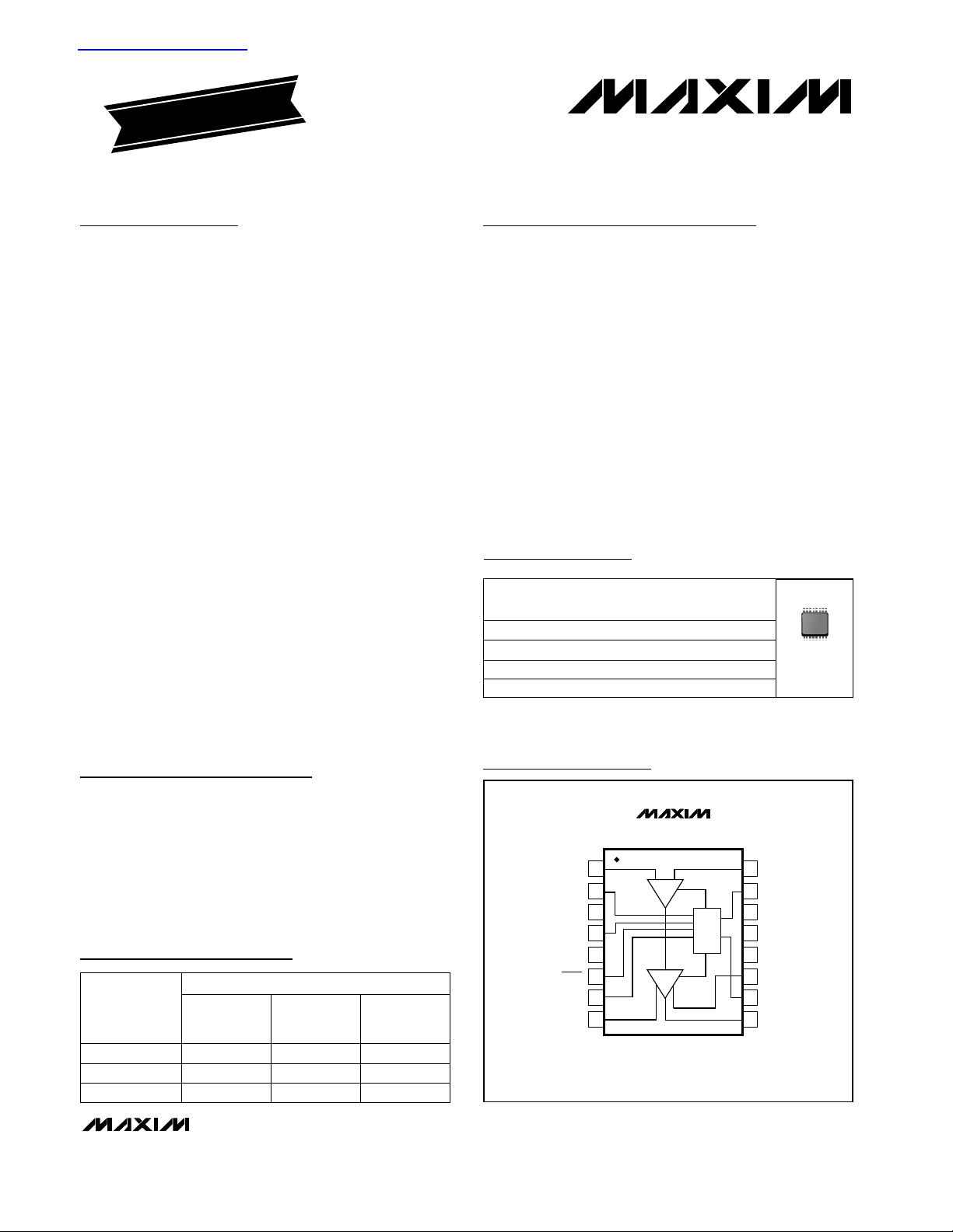
Pin Configurations
Ordering Information
Selector Guide
*Contact factory for dice specifications.
Pin Configurations continued at end of data sheet.
POWER-ADDED EFFICIENCY (%)
CDMA AT
+28dBm
CDMA AT
+16dBm
TDMA AT
+30dBm
—
427
1232
37MAX2265
MAX2264
DEVICE
16 TSSOP-EP
Dice*
16 TSSOP-EP
PIN-
PACKAGE
TEMP. RANGE
-40°C to +85°C
-40°C to +85°C
-40°C to +85°C
MAX2265EUE
MAX2264E/D
MAX2264EUE
16 TSSOP-EP-40°C to +85°C
MAX2266EUE
—
1732MAX2266
TSSOP-EP
5mm x 6.4mm
查询MAX2264供应商
TOP VIEW
IN1 IN0
1
PWR
2
V
3
CC
4
BIAS1H
V
5
CC
SHDN
6
BIAS2L
7
OUT1
8
MAX2264/MAX2266
16
BIAS2H
15
V
14
BIAS
TSSOP-EP
CC
GND
13
NFP
12
OUT0
11
BIAS1L
10
OUT1
9
MAX2264/MAX2265/MAX2266
2.7V, Single-Supply, Cellular-Band
Linear Power Amplifiers
2 _______________________________________________________________________________________
ABSOLUTE MAXIMUM RATINGS
DC ELECTRICAL CHARACTERISTICS
(VCC= +2.7V to +5V, TA= T
MIN
to T
MAX
, no input signal applied, V
SHDN
= 2.0V. Typical values are at VCC= +3.3V and TA= +25°C,
unless otherwise noted.)
Stresses beyond those listed under “Absolute Maximum Ratings” may cause permanent damage to the device. These are stress ratings only, and functional
operation of the device at these or any other conditions beyond those indicated in the operational sections of the specifications is not implied. Exposure to
absolute maximum rating conditions for extended periods may affect device reliability.
VCCto GND (no RF input) ....................................-0.3V to +6.5V
Logic Inputs to GND...................................-0.3V to (VCC+ 0.3V)
BIAS_ _ to GND..........................................-0.3V to (VCC+ 0.3V)
RF Input Power .................................................+13dBm (20mW)
Logic Input Current...........................................................±10mA
Output VSWR with +13dBm Input ........................................2.5:1
Total DC Power Dissipation (T
PADDLE
= +100°C)
16-Pin TSSOP-EP (derate 60mW/°C
above T
PADDLE
= +100°C) ...............................................4W
θJA ...............................................................................8°C/W
Operating Temperature Range ...........................-40°C to +85°C
Junction Temperature......................................................+150°C
Storage Temperature Range .............................-65°C to +150°C
Lead Temperature (soldering, 10sec) .............................+300°C
AC ELECTRICAL CHARACTERISTICS—MAX2264
(MAX2264 EV kit, VCC= V
PWR
= V
SHDN
= +3.3V, TA= +25°C, fIN= 836MHz, CDMA modulation, SHDN = VCC, matching networks
tuned for 824MHz to 849MHz operation, 50Ω system, unless otherwise noted.)
PWR = GND
PWR = V
CC
PARAMETER SYMBOL MIN TYP MAX UNITS
Logic Input Current Low
-1 1
µA
Logic Input Current High
-1 5
µA
Shutdown Supply Current I
CC
0.5 10
µA
83
Logic Threshold High
2.0
V
Logic Threshold Low
0.8
V
Idle Current
Operating Voltage Range V
CC
2.7 5.0
V
I
CC
95
34
CONDITIONS
Logic = GND
Logic = V
CC
SHDN = PWR = GND
MAX2265
MAX2264/MAX2266
mA
PARAMETER SYMBOL MIN TYP MAX UNITS
Output Power
(Low-Power Mode) (Note 1)
P
OUT
15 16.5
dBm
26 27
Output Power
(High-Power Mode) (Note 1)
P
OUT
27 28
dBm
18 21
14 15.5
Power Gain (Note 1)
Frequency Range (Notes 1, 2) f
IN
824 849
MHz
G
P
23 24.5
dB
22
CONDITIONS
PWR = GND, PINadjusted to meet ACPR
specification, f
IN
= 824MHz to 849MHz
PWR = VCC= 2.8V, PINadjusted to meet
ACPR specification, f
IN
= 824MHz to 849MHz
PWR = VCC, PINadjusted to meet ACPR
specification, f
IN
= 824MHz to 849MHz
PWR = GND
PWR = GND, VCC= 2.8V, PINadjusted to meet
ACPR specification, f
IN
= 824MHz to 849MHz
PWR = VCCor GND
PWR = V
CC
TA= +25°C
TA= T
MIN
to T
MAX
Gain Variation vs. Temperature
(Note 1)
±0.8 dBTA= T
MIN
to T
MAX
, relative to TA= +25°C
MAX2264/MAX2265/MAX2266
2.7V, Single-Supply, Cellular-Band
Linear Power Amplifiers
_______________________________________________________________________________________ 3
PARAMETER SYMBOL MIN TYP MAX UNITS
AMPS Output Power (Note 1) P
OUT
30.5 31 dBm
Adjacent-Channel Power Ratio
Limit (Notes 1, 2)
ACPR -44 dBc
Alternate-Channel Power Ratio
Limit (Notes 1, 2)
ACPR -56 dBc
AMPS Power-Added Efficiency PAE 44 %
Power-Mode Switching Time 550 ns
Turn-On Time (Notes 1, 4) 15µs
Maximum Input VSWR VSWR
Nonharmonic Spurious due
to Load Mismatch (Notes 1, 5)
-60 dBc
Noise Power (Note 6)
-139
-136
AMPS Noise Power (Note 6) -138 dBm/Hz
Harmonic Suppression 32 dBc
CONDITIONS
PIN= 8dBm
PIN= 8dBm
(Note 4)
VCC= 2.8V to 5.0V, offset = 885kHz,
30kHz BW, f
IN
= 824MHz to 849MHz
VCC= 2.8V to 5.0V, offset = 1980kHz,
30kHz BW, f
IN
= 824MHz to 849MHz
PWR = VCCor GND
fIN= 824MHz to 849MHz, PWR = GND or V
CC
PIN= 10dBm
Measured at 881MHz
PWR = GND, measured at 881MHz
Measured at 881MHz, PIN= 8dBm
(Note 7)
dBm/Hz
PARAMETER SYMBOL MIN TYP MAX UNITS
26 26.5
Output Power (Note 1) P
OUT
27 28
dBm
Gain Variation vs. Temperature
(Note 1)
±0.7 dB
AMPS Output Power (Note 1) P
OUT
30 31 dBm
Adjacent-Channel Power Ratio
(Notes 1, 2)
ACPR -44 -45 dBc
Alternate-Channel Power Ratio
(Notes 1, 2)
ACPR -56 -57 dBc
Frequency Range (Notes 1, 2) f
IN
824 849
MHz
23
CONDITIONS
VCC= 2.8V, PINadjusted to meet ACPR
specification, f
IN
= 824MHz to 849MHz
PINadjusted to meet ACPR specification,
f
IN
= 824MHz to 849MHz
TA= T
MIN
to T
MAX
, relative to TA= +25°C
PIN= 8dBm
VCC= 2.8V to 5.0V, offset = 885kHz,
30kHz BW, f
IN
= 824MHz to 849MHz
VCC= 2.8V to 5.0V, offset = 1980kHz,
30kHz BW, f
IN
= 824MHz to 849MHz
TA= T
MIN
to T
MAX
Power Gain (Note 1) G
P
24 25.5
dB
TA= +25°C
AC ELECTRICAL CHARACTERISTICS—MAX2264 (continued)
(MAX2264 EV kit, VCC= V
PWR
= V
SHDN
= +3.3V, TA= +25°C, fIN= 836MHz, CDMA modulation, SHDN = VCC, matching networks
tuned for 824MHz to 849MHz operation, 50Ω system, unless otherwise noted.)
32
PWR = VCC, PINadjusted to meet ACPR
specification
Power-Added Efficiency
(Note 3)
PAE
12
%
PWR = GND, PINadjusted to meet ACPR
specification
AC ELECTRICAL CHARACTERISTICS—MAX2265
(MAX2265 EV kit, VCC= V
SHDN
= +3.3V, TA= +25°C, fIN= 836MHz, CDMA modulation, matching networks tuned for 824MHz to
849MHz operation, 50Ω system, unless otherwise indicated.)
2.4:1
MAX2264/MAX2265/MAX2266
2.7V, Single-Supply, Cellular-Band
Linear Power Amplifiers
4 _______________________________________________________________________________________
AC ELECTRICAL CHARACTERISTICS—MAX2265 (continued)
(MAX2265 EV kit, VCC= V
SHDN
= +3.3V, TA= +25°C, fIN= 836MHz, CDMA modulation, matching networks tuned for 824MHz to
849MHz operation, 50Ω system, unless otherwise indicated.)
PARAMETER SYMBOL MIN TYP MAX UNITS
Power-Added Efficiency
(Note 3)
PAE
37
%
7
AMPS Power-Added Efficiency PAE 48 %
Turn-On Time (Notes 1, 4) 15µs
Maximum Input VSWR VSWR 1.3:1
Nonharmonic Spurious Due
to Load Mismatch (Notes 1, 5)
-60 dBc
Noise Power (Note 6) -140 dBm/Hz
AMPS Noise Power (Note 6) -139 dBm/Hz
Harmonic Suppression 47 dBc
CONDITIONS
PINadjusted to give P
OUT
= 28dBm
PINadjusted for P
OUT
= 16dBm
PIN= 8dBm
fIN= 824MHz to 849MHz
PIN= 10dBm
Measured at 881MHz
Measured at 881MHz, PIN= 8dBm
(Note 7)
AC ELECTRICAL CHARACTERISTICS—MAX2266
(MAX2266 EV kit, VCC= V
SHDN
= +3.3V, TA= +25°C, fIN= 836MHz, CDMA modulation, matching networks tuned for 824MHz to
849MHz operation, 50Ω system, unless otherwise indicated.)
PARAMETER SYMBOL MIN TYP MAX UNITS
Output Power
(Low-Power Mode) (Note 1)
P
OUT
14 15.5
dBm
26 27
Output Power
(High-Power Mode) (Note 1)
P
OUT
27 28
dBm
25 27.5
13 14
Power Gain (Note 1)
Frequency Range (Notes 1, 2) f
IN
824 849
MHz
G
P
24.5 26
dB
23
CONDITIONS
PWR = GND, PINadjusted to meet ACPR
specification, f
IN
= 824MHz to 849MHz
PWR = VCC= 2.8V, PINadjusted to meet
ACPR specification, f
IN
= 824MHz to 849MHz
PWR = VCC, PINadjusted to meet ACPR
specification, f
IN
= 824MHz to 849MHz
PWR = GND
PWR = GND, VCC= 2.8V, PINadjusted to meet
ACPR specification, f
IN
= 824MHz to 849MHz
PWR = VCCor GND
PWR = V
CC
Gain Variation vs. Temperature
(Note 1)
±0.8 dBTA= T
MIN
to T
MAX
, relative to TA= +25°C
TA= +25°C
TA= T
MIN
to T
MAX
Power-Added Efficiency
(Note 3)
PAE
32
%
17
PWR = VCC, PINadjusted to meet ACPR
specification
PWR = GND, PINadjusted to meet ACPR
specification
AMPS Output Power (Note 1) P
OUT
31 32 dBmPIN= 8dBm
Alternate-Channel Power Ratio
Limit (Notes 1, 2)
ACPR -56 dBc
VCC= 2.8V to 5.0V, offset = 1980kHz,
30kHz BW, f
IN
= 824MHz to 849MHz
Adjacent-Channel Power Ratio
Limit (Notes 1, 2)
ACPR -44 dBc
VCC= 2.8V to 5.0V, offset = 885kHz,
30kHz BW, f
IN
= 824MHz to 849MHz
MAX2264/MAX2265/MAX2266
2.7V, Single-Supply, Cellular-Band
Linear Power Amplifiers
_______________________________________________________________________________________ 5
Note 1: Minimum and maximum values are guaranteed by design and characterization, not production tested.
Note 2: P
MAX
is met over this frequency range at the ACPR limit with a single matching network. For optimum performance at other
frequencies, the output matching network must be properly designed. See the Applications Information section. Operation
between 750MHz and 1000MHz is possible but has not been characterized.
Note 3: PAE is specified into a 50Ω load, while meeting ACPR requirements.
Note 4: Time from logic transition until P
OUT
is within 1dB of its final mean power.
Note 5: Murata isolator as load with 20:1 VSWR any phase angle after isolator.
Note 6: Noise power can be improved by using the circuit in Figures 1, 2, and 3.
Note 7: Harmonics measured on evaluation kit, which provides some harmonic attenuation in addition to the rejection provided by
the IC. The combined suppression is specified.
PARAMETER SYMBOL MIN TYP MAX UNITS
AMPS Power-Added Efficiency PAE 48 %
Power-Mode Switching Time 550 ns
Turn-On Time (Notes 1, 4) 15µs
Maximum Input VSWR VSWR 2.4:1
Nonharmonic Spurious due
to Load Mismatch (Notes 1, 5)
-60 dBc
Noise Power (Note 6)
-137
-130
AMPS Noise Power (Note 6) -136 dBm/Hz
Harmonic Suppression 32 dBc
CONDITIONS
PIN= 8dBm
(Note 4)
PWR = VCCor GND
fIN= 824MHz to 849MHz, PWR = GND or V
CC
PIN= 10dBm
Measured at 881MHz
PWR = GND, measured at 881MHz
Measured at 881MHz, PIN= 8dBm
(Note 7)
dBm/Hz
AC ELECTRICAL CHARACTERISTICS—MAX2266 (continued)
(MAX2266 EV kit, VCC= V
PWR
= V
SHDN
= +3.3V, TA= +25°C, fIN= 836MHz, CDMA modulation, SHDN = VCC, matching networks
tuned for 824MHz to 849MHz operation, 50Ω system, unless otherwise noted.)
Typical Operating Characteristics
(MAX2264/MAX2265/MAX2266 EV kits, VCC= +3.3V, SHDN = VCC, CDMA modulation, TA= +25°C, unless otherwise noted.)
0
20
40
60
80
100
120
140
2.5 3.53.0 4.0 4.5 5.0 5.5
MAX2264
SHUTDOWN CURRENT vs. SUPPLY VOLTAGE
MAX2264-01
SUPPLY VOLTAGE (V)
SUPPLY CURRENT (nA)
TA = +85°C
TA = -40°C
TA = +25°C
PWR = GND
SHDN = GND
NO INPUT DRIVE
20
22
26
24
28
30
2.5 3.53.0 4.0 4.5 5.0
MAX2264
GAIN vs. SUPPLY VOLTAGE
MAX2264-02
SUPPLY VOLTAGE (V)
GAIN (dB)
PWR = V
CC
TA = -40°C
TA = +85°C
TA = +25°C
18
20
24
22
26
28
2.5 4.03.0
3.5
4.5 5.0
MAX2264
GAIN vs. SUPPLY VOLTAGE
MAX2264-03
SUPPLY VOLTAGE (V)
GAIN (dB)
PWR = GND
TA = -40°C
TA = +85°C
TA = +25°C

MAX2264/MAX2265/MAX2266
2.7V, Single-Supply, Cellular-Band
Linear Power Amplifiers
6 _______________________________________________________________________________________
Typical Operating Characteristics (continued)
(MAX2264/MAX2265/MAX2266 EV kits, VCC= +3.3V, SHDN = VCC, CDMA modulation, TA= +25°C, unless otherwise noted.)
36
PWR = V
34
32
PAE (%)
30
28
26
2.5 3.53.0 4.0 4.5 5.0
OUTPUT POWER vs. INPUT POWER
20
PWR = GND
16
12
OUTPUT POWER (dBm)
8
4
-14 -8-12
SUPPLY CURRENT vs. OUTPUT POWER
800
PWR = V
600
V
CC
400
AT T
SUPPLY CURRENT (mA)
200
MAX2264
POWER-ADDED EFFICIENCY
vs. SUPPLY VOLTAGE
CC
TA = +85°C
SUPPLY VOLTAGE (V)
TA = -40°C
TA = +25°C
MAX2264
TA = -40°C
TA = +25°C
TA = +85°C
-10
INPUT POWER (dBm)
-6 -4 -2
MAX2264
CC
= 2.7V/3.3V
= -40°C/+25°C/+85°C
A
MAX2264-04
PAE (%)
MAX2264-07
GAIN (dB)
160
MAX2264-10
120
SUPPLY CURRENT (mA)
MAX2264
POWER-ADDED EFFICIENCY
vs. SUPPLY VOLTAGE
14
13
12
11
10
9
8
2.5 4.03.0
PWR = GND
TA = +25°C
3.5
SUPPLY VOLTAGE (V)
TA = -40°C
TA = +85°C
4.5 5.0
MAX2264
GAIN vs. OUTPUT POWER
27
26
25
24
23
22
PWR = V
V
CC
T
A
0155
V
T
= +25°C
V
CC
CC
T
A
= 2.7V
CC
= -40°C
A
= 3.3V
V
= 2.7V
CC
= +25°C
T
A
10
OUTPUT POWER (dBm)
= 3.3V
= -40°C
V
CC
= +85°C
T
A
V
= 2.7V
CC
= +85°C
T
A
20 25
= 3.3V
MAX2264
SUPPLY CURRENT vs. OUTPUT POWER
PWR = GND
TA = +85°C
80
40
TA = +25°C
TA = -40°C
OUTPUT POWER vs. INPUT POWER
MAX2264
32
PWR = V
MAX2264-05
OUTPUT POWER (dBm)
31
30
29
28
27
26
25
CC
V
= 3.3V
CC
= +25°C
T
A
V
= 3.3V
CC
= -40°C
T
A
V
= 2.7V
CC
= +85°C
T
A
04
2
INPUT POWER (dBm)
MAX2264
GAIN vs. OUTPUT POWER
25
MAX2264-08
30
35
24
23
GAIN (dB)
22
21
20
PWR = GND
-10 5-5
TA = +25°C
0
OUTPUT POWER (dBm)
MAX2264
ADJACENT-CHANNEL POWER RATIO
vs. OUTPUT POWER
-30
PWR = V
MAX2264-11
-40
-50
ACPR (dBc)
-60
-70
CC
TA = +85°C
TA = +25°C
V
= 3.3V
CC
= +85°C
T
A
V
= 2.7V
CC
= +25°C
T
A
TA = -40°C
TA = +85°C
10 15 20
TA = -40°C
MAX2264-06
V
= 2.7V
CC
= -40°C
T
A
68
MAX2264-09
MAX2264-12
0
0155
10
OUTPUT POWER (dBm)
20 25
0
30
35
093
6
OUTPUT POWER (dBm)
12 15 18
-80
-20 0-10 10 20 30
OUTPUT POWER (dBm)
MAX2264/MAX2265/MAX2266
2.7V, Single-Supply, Cellular-Band
Linear Power Amplifiers
_______________________________________________________________________________________ 7
Typical Operating Characteristics (continued)
(MAX2264/MAX2265/MAX2266 EV kits, VCC= +3.3V, SHDN = VCC, CDMA modulation, TA= +25°C, unless otherwise noted.)
0
20
40
60
80
100
120
140
2.5 3.53.0 4.0 4.5 5.0 5.5
MAX2265
SHUTDOWN CURRENT
vs. SUPPLY VOLTAGE
MAX2265-18
SUPPLY VOLTAGE (V)
SUPPLY CURRENT (nA)
TA = +85°C
TA = -40°C
TA = +25°C
PWR = GND
SHDN = GND
NO INPUT DRIVE
20
22
26
24
28
30
2.5 3.53.0 4.0 4.5 5.0
MAX2265
GAIN vs. SUPPLY VOLTAGE
MAX2265-19
SUPPLY VOLTAGE (V)
GAIN (dB)
TA = -40°C
TA = +85°C
TA = +25°C
29
31
35
33
37
39
2.5 3.53.0 4.0 4.5 5.0
MAX2265
POWER-ADDED EFFICIENCY
vs. SUPPLY VOLTAGE
MAX2265-20
SUPPLY VOLTAGE (V)
PAE (%)
TA = +25°C
TA = +85°C
TA = -40°C
25
28
27
26
29
30
31
32
04
2
68
MAX2265
OUTPUT POWER
vs. INPUT POWER
MAX2265-21
INPUT POWER (dBm)
OUTPUT POWER (dBm)
V
CC
= 3.3V
T
A
= +85°C
V
CC
= 3.3V
T
A
= +25°C
V
CC
= 2.7V
T
A
= +25°C
V
CC
= 3.3V
T
A
= -40°C
V
CC
= 2.7V
T
A
= +85°C
V
CC
= 2.7V
T
A
= -40°C
MAX2264
ADJACENT-CHANNEL POWER RATIO
vs. OUTPUT POWER
MAX2264-13
55
50
PWR = V
= T
T
A
45
40
35
30
25
PAE (%)
20
15
10
5
0
51015
020
POWER-ADDED EFFICIENCY
-40
-45
-50
ACPR (dBc)
-55
-60
-65
-10 5-5
PWR = GND
TA = +25°C
TA = +85°C
TA = -40°C
0
OUTPUT POWER (dBm)
MAX2264
POWER-ADDED EFFICIENCY
10 15 20
vs. FREQUENCY
MAX2264-16
15
10
PAE (%)
5
PWR = GND
= 16dBm
P
OUT
11%
40
38
36
PAE (%)
34
32
PWR = V
P
OUT
32.0%
CC
= 28dBm
32.7%
33.2%
33.1%
33.0%
MAX2264
POWER-ADDED EFFICIENCY
vs. OUTPUT POWER
CC
TO T
MIN
MAX
V
= 2.7V
CC
V
= 3.3V
CC
25
OUTPUT POWER (dBm)
MAX2264
vs. FREQUENCY
12%
12%
12%
30 35
11%
MAX2264-14
MAX2264-17
16
12
8
PAE (%)
4
0
PWR = GND
-10 5-5
MAX2264
POWER-ADDED EFFICIENCY
vs. OUTPUT POWER
TA = +85°C
TA = +25°C
TA = -40°C
0
OUTPUT POWER (dBm)
10 15 20
MAX2264-15
30
824 836830 842 848
0
824 836830 842 848
FREQUENCY (MHz)
FREQUENCY (MHz)

MAX2264/MAX2265/MAX2266
2.7V, Single-Supply, Cellular-Band
Linear Power Amplifiers
8 _______________________________________________________________________________________
Typical Operating Characteristics (continued)
(MAX2264/MAX2265/MAX2266 EV kits, VCC= +3.3V, SHDN = VCC, CDMA modulation, TA= +25°C, unless otherwise noted.)
30
32
36
34
38
40
826 836831 841 846
MAX2265
POWER-ADDED EFFICIENCY
vs. FREQUENCY
MAX2265-26
PAE (%)
36.75%
36.58%
36.74%
36.38%
36.50%
-60
-40
-50
-20
-30
0
-10
10
30
20
40
CENTER 836MHz
MAX2265
TDMA POWER SPECTRUM
MAX2265-27
15.2805kHz/div
SPAN 152.805kHz
POWER (dBm)
0
20
40
60
80
100
120
140
2.5 3.53.0 4.0 4.5 5.0 5.5
MAX2266
SHUTDOWN CURRENT vs. SUPPLY VOLTAGE
MAX2266-01
SUPPLY VOLTAGE (V)
SUPPLY CURRENT (nA)
TA = +85°C
TA = -40°C
TA = +25°C
PWR = GND
SHDN = GND
NO INPUT DRIVE
20
22
26
24
28
30
2.5 3.0 3.5 4.0 4.5 5.0
MAX2266
GAIN vs. SUPPLY VOLTAGE
MAX2266 toc02
SUPPLY VOLTAGE (V)
GAIN (dB)
PWR = V
CC
TA = +25°C
TA = -40°C
TA = +85°C
24
26
30
28
32
34
2.5 3.0 3.5 4.0 4.5 5.0
MAX2266
GAIN vs. SUPPLY VOLTAGE
MAX2266 toc03
SUPPLY VOLTAGE (V)
GAIN (dB)
PWR = GND
PIN = SET FOR ACPR LIMIT
TA = +25°C
TA = -40°C
TA = +85°C
MAX2265
GAIN vs. OUTPUT POWER
27
V
26
T
= 2.7V
CC
= -40°C
A
V
CC
= -40°C
T
A
= 3.3V
MAX2265-22
SUPPLY CURRENT vs. OUTPUT POWER
800
600
MAX2265
MAX2265-23
ADJACENT-CHANNEL POWER RATIO
-30
VCC = 3.3V
-40
MAX2265
vs. OUTPUT POWER
TA = +85°C
MAX2265-24
25
GAIN (dB)
24
23
22
V
CC
T
A
0155
= 3.3V
= +25°C
V
CC
T
A
10
OUTPUT POWER (dBm)
= 2.7V
= +25°C
V
CC
= +85°C
T
A
V
= 2.7V
CC
= +85°C
T
A
20 25
= 3.3V
SUPPLY CURRENT (mA)
30
35
400
200
0
0155
V
AT T
CC
= 2.7V/3.3V
= -40°C/+25°C/+85°C
A
USING OPTIONAL TB
CIRCUIT IN FIGURE 2
10
OUTPUT POWER (dBm)
20 25
MAX2265
POWER-ADDED EFFICIENCY
vs. OUTPUT POWER
55
50
45
40
35
30
25
PAE (%)
20
15
10
5
0
51015
020
V
= 2.7V
CC
= -40°C
T
A
V
= 2.7V
CC
= +25°C
T
A
V
= 2.7V
CC
= +85°C
T
A
V
= 3.3V
CC
= -40°C
T
A
V
T
OUTPUT POWER (dBm)
V
T
= 3.3V
CC
= +25°C
A
25
= 3.3V
CC
= +85°C
A
30 35
MAX2265-25
-50
ACPR (dBc)
-60
-70
-80
30
35
-20 0-10 10 20 30
TA = +25°C
OUTPUT POWER (dBm)
TA = -40°C

MAX2264/MAX2265/MAX2266
2.7V, Single-Supply, Cellular-Band
Linear Power Amplifiers
_______________________________________________________________________________________ 9
Typical Operating Characteristics (continued)
(MAX2264/MAX2265/MAX2266 EV kits, VCC= +3.3V, SHDN = VCC, CDMA modulation, TA= +25°C, unless otherwise noted.)
MAX2266
POWER-ADDED EFFICIENCY
vs. SUPPLY VOLTAGE
MAX2266 toc04
20
PWR = GND
19
18
17
PAE (%)
16
15
14
2.5 3.53.0 4.0 4.5 5.0
36
PWR = V
CC
34
TA = -40°C
32
PAE (%)
30
TA = +25°C
TA = +85°C
28
26
2.5 3.0 3.5 4.0 4.5 5.0
SUPPLY VOLTAGE (V)
MAX2266
OUTPUT POWER vs. INPUT POWER
24
PWR = GND
TA = -40°C
20
TA = +25°C
16
OUTPUT POWER (dBm)
12
TA = +85°C
8
-14 -8-12 -10 -6 -4 -2
INPUT POWER (dBm)
MAX2266 toc07
27
PWR = V
26
25
GAIN (dB)
24
23
22
0105 1520253035
MAX2266
SUPPLY CURRENT vs. OUTPUT POWER
800
PWR = V
CC
600
VCC = 2.7V/3.3V
= -40°C/+25°C/+85°C
AT T
400
SUPPLY CURRENT (mA)
200
A
MAX2266 toc10
SUPPLY CURRENT vs. OUTPUT POWER
160
PWR = GND
120
80
SUPPLY CURRENT (mA)
40
MAX2266
POWER-ADDED EFFICIENCY
vs. SUPPLY VOLTAGE
TA = -40°C
TA = +25°C
TA = +85°C
SUPPLY VOLTAGE (V)
MAX2266
GAIN vs. OUTPUT POWER
VCC = 3.3V
CC
TA = -40°C
VCC = 2.7V
TA = -40°C
VCC = 3.3V
TA = +85°C
VCC = 2.7V
CC
= 3.3V
TA = +85°C
VCC = 2.7V
TA = +25°C
V
TA = +25°C
OUTPUT POWER (dBm)
MAX2266
TA = +85°C
TA = +25°C
TA = -40°C
MAX2266 toc05
OUTPUT POWER (dBm)
MAX2266 toc08
GAIN (dB)
-30
MAX2266 toc11
-40
-50
ACPR (dBc)
-60
-70
OUTPUT POWER vs. INPUT POWER
MAX2266
32
PWR = V
CC
VCC = 3.3V
= +85°C
T
31
30
VCC = 3.3V
TA = -40°C
29
28
27
26
25
0231 45678
VCC = 3.3V
T
= +25°C
A
A
VCC = 2.7V
TA = +85°C
V
= 2.7V
CC
TA = +25°C
VCC = 2.7V
TA = -40°C
INPUT POWER (dBm)
MAX2266
GAIN vs. OUTPUT POWER
30
PWR = GND
TA = -40°C
29
28
TA = +25°C
27
26
25
TA = +85°C
-10 -5 0 5 10 15 20
OUTPUT POWER (dBm)
MAX2266
ADJACENT-CHANNEL POWER RATIO
vs. OUTPUT POWER
PWR = V
CC
TA = +25°C
TA = +85°C
TA = -40°C
MAX2266 toc06
MAX2266 toc09
MAX2266 toc12
0
015205 10 253035
OUTPUT POWER (dBm)
0
093 6 12 15 18
OUTPUT POWER (dBm)
-80
-20 -10 0 10 20 30
OUTPUT POWER (dBm)

MAX2264/MAX2265/MAX2266
2.7V, Single-Supply, Cellular-Band
Linear Power Amplifiers
10 ______________________________________________________________________________________
Typical Operating Characteristics (continued)
(MAX2264/MAX2265/MAX2266 EV kits, VCC= +3.3V, SHDN = VCC, CDMA modulation, TA= +25°C, unless otherwise noted.)
ADJACENT-CHANNEL POWER RATIO
MAX2266
vs. OUTPUT POWER
-30
PWR = GND
-40
-50
ACPR (dBc)
-60
-70
-80
-10 -5 0 5 10 15 20
TA = +85°C
TA = +25°C
TA = -40°C
MAX2266 toc13
55
PWR = V
50
45
40
35
30
25
PAE (%)
20
15
10
5
0
0 5 10 15 20 25 30 35
MAX2266
POWER-ADDED EFFICIENCY
vs. OUTPUT POWER
CC
VCC = 2.7V
VCC = 3.3V
OUTPUT POWER (dBm)
MAX2266 toc14
20
PWR = GND
15
10
PAE (%)
5
0
-10 5-5 0 101520
MAX2266
POWER-ADDED EFFICIENCY
vs. OUTPUT POWER
TA = +25°C
TA = -40°C
TA = +85°C
OUTPUT POWER (dBm)
MAX2266 toc15
MAX2266
POWER-ADDED EFFICIENCY
vs. FREQUENCY
38
PWR = V
CC
P
= 28dBm
OUT
36
34
PAE (%)
32
30
28
31.6%
31.3%
824 836830 842 848
FREQUENCY (MHz)
31.9%
32.2%
MAX2266 toc16
32.4%
25
PWR = GND
P
20
17.6%
15
PAE (%)
10
5
MAX2266
POWER-ADDED EFFICIENCY
vs. FREQUENCY
= 16dBm
OUT
17.4%
17.3%
17.0%
16.9%
824 836830 842 848
FREQUENCY (MHz)
MAX2266 toc17

MAX2264/MAX2265/MAX2266
2.7V, Single-Supply, Cellular-Band
Linear Power Amplifiers
______________________________________________________________________________________ 11
Detailed Description
The MAX2264/MAX2265/MAX2266 are linear power
amplifiers (PAs) intended for CDMA and TDMA applications. The devices have been fully characterized in
the 824MHz to 849MHz U.S. cellular band and can be
used from 750MHz to 1000MHz by adjusting the input
and output match. In CDMA applications, they provide
typically 28dBm of output power and up to 37% poweradded efficiency (PAE) from a single +2.7V to +5V supply. In TDMA applications, efficiency is 42% at 30dBm
of output power.
An inherent drawback of traditional PAs is that their efficiency drops rapidly with reduced output power. For
example, in a PA designed for maximum efficiency at
+28dBm, the efficiency at +15dBm falls well below
4.5% (over 210mA from a +3.3V supply). This behavior
significantly reduces talk time in CDMA phones
because over 90% of the time they are at output powers below +16dBm. The MAX2264/MAX2265/MAX2266
are optimized for lowest current draw at output powers
that are most likely to occur in real-life situations. This
provides up to 50% reduced average PA current.
High-Power and Low-Power Modes
The MAX2264/MAX2266 are designed to provide optimum PAE in both high- and low-power modes. For a
+3.3V supply, maximum output power is +28dBm in
high-power mode and +16dBm in low-power mode.
Use the system’s microcontroller to determine required
output power, and switch between the two modes as
appropriate with the PWR logic pin.
Bias Control
The bias current of the first stage in low-power mode is
proportional to the current flowing out of BIAS1L. The
voltage at BIAS1L is fixed by an internal bandgap refer-
Pin Description
IN0 RF Input Port. Requires external matching network.—16
BIAS1L
OUT0
NFP
GND
BIAS2H
BIAS1H
SHDN
BIAS2L
OUT1
V
CC
PWR
IN1
NAME
Low-Power Mode First Stage Bias Control. See General Description.—10
RF Output Port. Requires an appropriate output matching network and collector
bias.
—11
Noise Filtering Pin. Connect noise filtering network as described in
Noise Filtering section. If unused, leave open.
1212
Ground. Solder the package slug to high-thermal-conductivity circuit board
ground plane.
13, Slug13, Slug
High-Power Mode Second Stage Bias Control. See General Description.1515
High-Power Mode First Stage Bias Control. See General Description.44
Shutdown Control Input. Drive SHDN low to enable shutdown. Drive high for normal
operation. On the MAX2265, make sure that both pins get driven simultaneously.
To place the MAX2264/MAX2266 into shutdown mode, also pull the PWR pin low.
2, 66
Low-Power Mode Second Stage Bias Control. See General Description.—7
RF Output Ports. Require an appropriate output matching network and collector
bias.
8, 98, 9
Voltage Supply. Bypass with capacitors connected between this pin and GND.3, 53, 5, 14
Mode-Select Input. Drive low to select the low-power mode (BIAS1L and
BIAS2L). Drive high to select high-power mode (BIAS1H and BIAS2H).
—2
PIN
RF Input Port. Requires external matching network.11
MAX2265
MAX2264
MAX2266
FUNCTION
N.C. Not Internally Connected. Do not make any connections to these pins.
7, 10, 11,
14, 16
—
MAX2264/MAX2265/MAX2266
2.7V, Single-Supply, Cellular-Band
Linear Power Amplifiers
12 ______________________________________________________________________________________
ence, so the current out of this pin is inversely proportional to the value of the resistor between this pin and
ground. Similarly, the bias current of the first stage in
high-power mode is proportional to the current flowing
out of BIAS1H. The current in the second stage is proportional to the currents out of BIAS2L and BIAS2H for
low- and high-power modes, respectively.
Additionally, these resistors allow for customization of
gain and alternate- and adjacent-channel power ratios.
Increasing the bias current in the first stage increases
the gain and improves alternate-channel power ratio at
the expense of efficiency. Increasing the bias current in
the second stage increases gain at the expense of efficiency as well as adjacent- and alternate-channel power
ratios.
The PA bias current can be dynamically adjusted by
summing a current into the bias pin of interest with an
external source such as a DAC. See the MAX2265
Typical Application Circuit for using a voltage DAC and
current setting resistors RTB1 and RTB2. Choosing
RTB1 = R1 and RTB2 = R2 allows current adjustment
between 0mA to double the nominal idle current with
DAC voltages between 0V and 2.4V. The DAC must be
able to source approximately 100µA.
Shutdown Mode
Pull pins 2 and 6 low to place the MAX2264/MAX2265/
MAX2266 into shutdown mode. In this mode, all gain
stages are disabled and supply current drops to 0.5µA.
Increasing Efficiency Further
The MAX2266 incorporates an additional external
switch to increase efficiency to 17% at +16dBm and to
32% at +28dBm. This efficiency increase is mainly due
to the additional isolation between the high- and lowpower outputs provided by the external switch.
Applications Information
External Components
The MAX2264/MAX2265/MAX2266 require matching
circuits at their inputs and outputs for operation in a
50Ω system. The application circuits in Figures 1, 2,
and 3 describe the topology of the matching circuits for
Figure 1. MAX2264 Typical Application Circuit
RFIN
L1
L2
C1
C2
MAX2264
L3
C3
C11
C12
V
SHDN
CC
PWR
V
V
1
2
CC
CC
RH1
RL2
L4
C4
3
4
5
6
7
8
BIAS
16
15
14
13
12
11
10
9
C7
RH2
V
C13
RL1
C9
CC
OPTIONAL NOISE-REDUCTION CIRCUIT
L6
C6
L5
C8
RFOUT
V
CC
C5
MAX2264/MAX2265/MAX2266
2.7V, Single-Supply, Cellular-Band
Linear Power Amplifiers
______________________________________________________________________________________ 13
Figure 2. MAX2265 Typical Application Circuit
each device; suggested component values, suppliers,
and part numbers are listed in Table 1. These values
are optimized for best simultaneous efficiency and
return loss performance. Use high-quality components
in these matching circuits for greatest efficiency.
Layout and Power-Supply Bypassing
A properly designed PC board is essential to any
RF/microwave circuit. Be sure to use controlled impedance lines on all high-frequency inputs and outputs.
Proper grounding of the GND pins is fundamental; if the
PC board uses a topside RF ground, connect all GND
pins (especially the TSSOP package exposed GND pad)
directly to it. On boards where the ground plane is not on
the component side, it’s best to connect all GND pins to
the ground plane with plated through-holes close to the
package.
To minimize coupling between different sections of the
system, the ideal power-supply layout is a star configuration with a large decoupling capacitor at a central
VCCnode. The VCCtraces branch out from this central
node, each leading to a separate VCCnode on the PC
board. A second bypass capacitor with low ESR at the
RF frequency of operation is located at the end of each
trace. This arrangement provides local decoupling at
the VCCpin.
Input and output impedance-matching networks are
very sensitive to layout-related parasitics. It is important
to keep all matching components as close to the IC as
possible to minimize the effects of stray inductance
and stray capacitance of PC board traces.
OPTIONAL TB CIRCUIT
TX
POWER
R
TB2
R
TB1
R1
C11
C12
V
SHDN
CC
C3
V
CC
V
CC
L3
C4
RFIN
L1
C1
L4
MAX2265
BIAS
16
15
14
13
12
11
10
9
C13
C9
R2
L7
OPTIONAL
NOISE-REDUCTION
CIRCUIT
1
2
3
4
5
6
7
8
L6
C6
C7
RFOUT

MAX2264/MAX2265/MAX2266
Noise Filtering
For improved noise performance, the MAX2264/
MAX2265/MAX2266 allow for additional noise filtering
for further suppression of transmit noise. This is
achieved by using C6 and L6 on the MAX2264, C13
and L7 on the MAX2265, and C6 and L6 on the
MAX2266. Use the recommended component values
for optimal noise power (Table 1).
2.7V, Single-Supply, Cellular-Band
Linear Power Amplifiers
14 ______________________________________________________________________________________
Figure 3. MAX2266 Typical Application Circuit
RFIN
C2
L1
L2
C1
MAX2266
L3
PWR
C3
C11
C12
V
V
SHDN
CC
V
CC
CC
RH1
RL2
L4
C4
1
2
3
4
5
6
7
8
C7
C9
BIAS
16
15
14
13
12
11
10
9
U1
UPG152TA
2
RL1
RH2
V
CC
C13
L6
C6
OPTIONAL NOISEREDUCTION CIRCUIT
V
L5
V
CC
3
6
4
5
C8
CC
C5
R1
PWR
Q1
OPTIONAL
RFOUT

MAX2264/MAX2265/MAX2266
2.7V, Single-Supply, Cellular-Band
Linear Power Amplifiers
______________________________________________________________________________________ 15
Chip Information
TRANSISTOR COUNT: 1256
Pin Configurations (continued)
TOP VIEW
IN1 N.C.
1
SHDN
2
V
3
CC
BIAS1H
4
V
5
CC
SHDN
6
N.C.
7
OUT1
8
MAX2265
TSSOP-EP
BIAS
16
BIAS2H
15
N.C.
14
GND
13
NFP
12
N.C.
11
N.C.
10
OUT1
9

MAX2264/MAX2265/MAX2266
2.7V, Single-Supply, Cellular-Band
Linear Power Amplifiers
NOTES
16 ______________________________________________________________________________________
 Loading...