

Page 1
For pricing, delivery, and ordering information, please contact Maxim/Dallas Direct! at
1-888-629-4642, or visit Maxim’s website at www.maxim-ic.com.
General Description
The MAX2242 low-voltage linear power amplifier (PA) is
designed for 2.4GHz ISM-band wireless LAN applications. It delivers +22.5dBm of linear output power with
an adjacent-channel power ratio (ACPR) of <-33dBc
1st-side lobe and <-55dBc 2nd-side lobe, compliant
with the IEEE 802.11b 11MB/s WLAN standard with at
least 3dB margin. The PA is packaged in the tiny 3x4
chip-scale package (UCSP™), measuring only 1.5mm x
2.0mm, ideal for radios built in small PC card and compact flash card form factors.
The MAX2242 PA consists of a three-stage PA, power
detector, and power management circuitry. The power
detector provides over 20dB of dynamic range with
±0.8dB accuracy at the highest output power level. An
accurate automatic level control (ALC) function can be
easily implemented using this detector circuit.
The PA also features an external bias control pin.
Through the use of an external DAC, the current can be
throttled back at lower output power levels while maintaining sufficient ACPR performance. As a result, the
highest possible efficiency is maintained at all power
levels. The device operates over a single +2.7V to
+3.6V power-supply range. An on-chip shutdown feature reduces operating current to 0.5µA, eliminating the
need for an external supply switch.
________________________Applications
IEEE 802.11b DSSS Radios
Wireless LANs
HomeRF
2.4GHz Cordless Phones
2.4GHz ISM Radios
Features
♦ 2.4GHz to 2.5GHz Operating Range
♦ +22.5dBm Linear Output Power (ACPR of <-33dBc
1st-Side Lobe and <-55dbc 2nd-Side Lobe)
♦ 28.5dB Power Gain
♦ On-Chip Power Detector
♦ External Bias Control for Current Throttleback
♦ +2.7V to +3.6V Single-Supply Operation
♦ 0.5µA Shutdown Mode
♦ Tiny Chip-Scale Package (1.5mm
✕
2.0mm)
MAX2242
2.4GHz to 2.5GHz Linear Power Amplifier
________________________________________________________________ Maxim Integrated Products 1
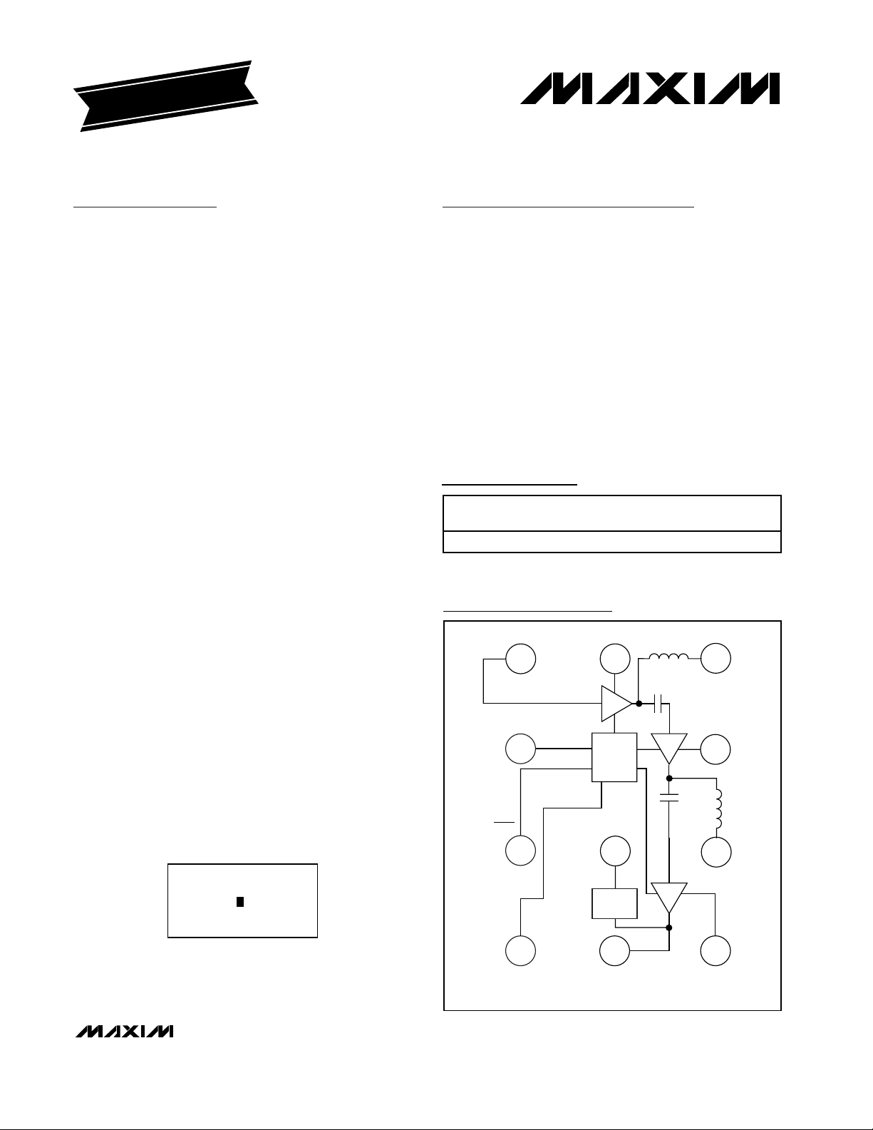
Pin Configuration
19-1912; Rev 3; 11/03
EVALUATION KIT
AVAILABLE
Ordering Information
Typical Application Circuit appears at end of data sheet.
Actual Size
1.5mm
✕
2.0mm
UCSP is a trademark of Maxim Integrated Products, Inc.
PART TEMP RANGE
MAX2242EBC-T -40°C to +85°C3
GNDRF_IN
B4C4
C3
V
CCB
BIAS
CIRCUIT
PIN-
PACKAGE
✕ 4 UCSP AAE
V
CC1
A4
GND
A3
MARK
TOP
PD_OUT
B2
DET
B1C1
RF_OUTBIAS
3✕4 UCSP
A2
A1
GND
SHDN
C2
V
CC2
Page 2
MAX2242
2.4GHz to 2.5GHz
Linear Power Amplifier
2 _______________________________________________________________________________________
ABSOLUTE MAXIMUM RATINGS
DC ELECTRICAL CHARACTERISTICS
(VCC= +2.7V to +3.6V, fIN= 2.4GHz to 2.5GHz, V
SHDN
= VCC, RF_IN = RF_OUT = connected to 50Ω load, TA= -40°C to +85°C.
Typical values are measured at V
CC
= +3.3V, fIN= 2.45GHz, TA= +25°C, unless otherwise noted.) (Note 1)
Stresses beyond those listed under “Absolute Maximum Ratings” may cause permanent damage to the device. These are stress ratings only, and functional
operation of the device at these or any other conditions beyond those indicated in the operational sections of the specifications is not implied. Exposure to
absolute maximum rating conditions for extended periods may affect device reliability.
V
CC1
, V
CC2
to GND (no RF signal applied) ..........-0.3V to +5.5V
RF Input Power ...............................................................+10dBm
SHDN, BIAS, PD_OUT, RF_OUT................-0.3V to (V
CC
+ 0.3V)
DC Input Current at RF_IN Port.............................-1mA to +1mA
Maximum VSWR Without Damage ........................................10:1
Maximum VSWR for Stable Operation.....................................5:1
Continuous Power Dissipation (T
A
= +85°C)
3
✕
4 UCSP (derate 80mW/°C above +85°C) ..................1.6W
Operating Temperature Range ...........................-40°C to +85°C
Thermal Resistance .........................................................25°C/W
Junction Temperature......................................................+150°C
Storage Temperature Range .............................-65°C to +125°C
Lead Temperature (soldering, 10s) .................................+260°C
Continuous Operating Lifetime.....................10yrs × 0.92
(TA- 60°C)
(For Operating Temperature, TA≥ +60°C)
CAUTION! ESD SENSITIVE DEVICE
PARAMETER CONDITIONS MIN TYP MAX UNITS
Supply Voltage 2.7 3.6 V
Supply Current
(Notes 2, 3, 6)
Shutdown Supply Current V
Logic Input Voltage High 2.0 V
Logic Input Voltage Low 0.8 V
Logic Input Current High -1 5 µA
Logic Input Current Low -1 1 µA
P
= +22dBm, VCC = +3.3V, idle current = 280mA
OUT
P
= +13dBm, idle current = 55mA 90
OUT
= +5dBm, idle current = 25mA 50
P
OUT
= 0, no RF input 0.5 10 µA
SHDN
300 335
mA
Page 3
MAX2242
2.4GHz to 2.5GHz
Linear Power Amplifier
_______________________________________________________________________________________ 3
AC ELECTRICAL CHARACTERISTICS
(MAX2242 Evaluation Kit, VCC= +3.3V, V
SHDN
= VCC, 50Ω source and load impedance, fIN= 2.45GHz, TA= +25°C, unless other-
wise noted.) (Note 6)
Note 1: Specifications over T
A
= -40°C to +85°C are guaranteed by design. Production tests are performed at TA= +25°C.
Note 2: Idle current is controlled by external DAC for best efficiency over the entire output power range.
Note 3: Parameter measured with RF modulation based on IEEE 802.11b standard.
Note 4: Power gain is guaranteed over this frequency range. Operation outside this range is possible, but is not guaranteed.
Note 5: Output two-tone third-order intercept point (OIP3) is production tested at T
A
= +25°C. The OIP3 is tested with two signals at
f1 = 2.450GHz and f2 = 2.451GHz with fixed P
IN
.
Note 6: Min/max limits are guaranteed by design and characterization.
Note 7: The total turn-on and turn-off times required for PA output power to settle to within 0.5dB of the final value.
Note 8: Excludes PC board loss of approximately 0.15dB.
Note 9: See Typical Operating Characteristics for statistical variation.
Frequency Range (Notes 3, 4) 2.4 2.5 GHz
Power Gain (Notes 1, 3)
Gain Variation Over Temperature
(Note 3)
Gain Variation Over V
(Note 3)
Output Power (Notes 3, 5, 8)
Saturated Output Power
Harmonic Output (2f, 3f, 4f) -40 dBc
Input VSWR Over full PIN range 1.5:1
Output VSWR Over full P
Power Ramp Turn-On Time
(Note 7)
Power Ramp Turn-Off Time
(Note 7)
RF Output Detector Response
TIme
RF Output Detector Voltage
PARAMETER CONDITIONS MIN TYP MAX UNITS
TA = +25°C 26.5 28.5
T
A
T
A
(±10%)
CC
V
CC
ACPR,
st-side lobe < -33dBc,
1
nd-side lobe < -55dBc
2
P
IN
SHDN from low to high 1 1.5 µs
SHDN from high to low 1 1.5 µs
Po = +22dBm (Note 9) 1.8
Po = +13dBm (Note 9) 0.9
P
o
= -40°C to +85°C 25.5
= -40°C to +85°C ±1.2 dB
= +3.0V to +3.6V ±0.3 dB
21.5 22.5 dBm
= +5dBm
range 2.5:1
OUT
= +5dBm (Note 9) 0.55
26.5 dBm
2.5 5 µs
dB
V
Page 4
MAX2242
2.4GHz to 2.5GHz
Linear Power Amplifier
4 _______________________________________________________________________________________
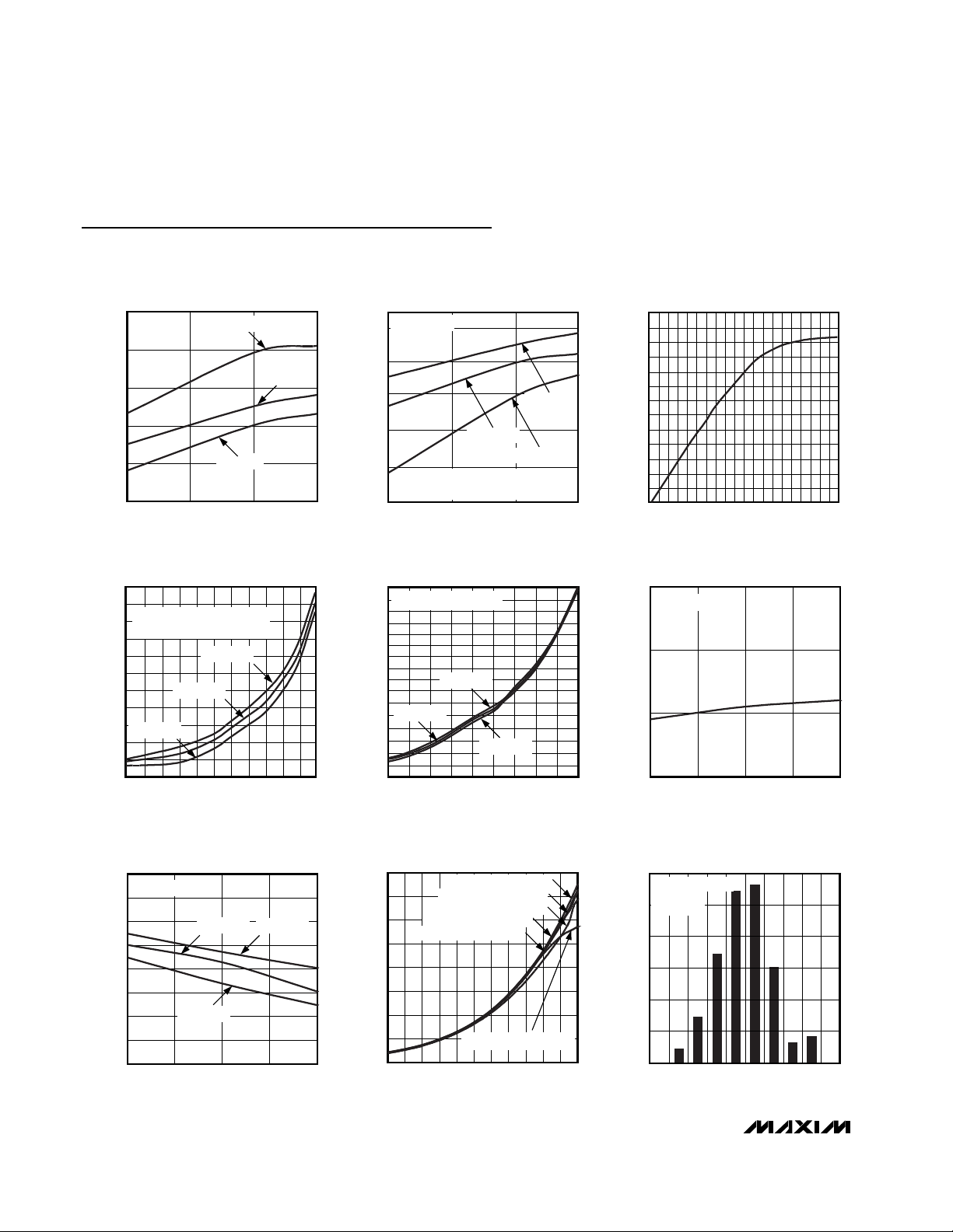
Typical Operating Characteristics
(VCC= +3.3V, fIN= 2.45MHz, RF modulation = IEEE 802.11b, V
SHDN
= VCC, TA= +25°C, unless otherwise noted.)
26
27
29
28
30
31
GAIN vs. SUPPLY VOLTAGE
MAX2242 toc01
SUPPLY VOLTAGE (V)
GAIN (dB)
2.7 3.33.0 3.6
PO = +22dBm
TA = +25°C
TA = +85°C
TA = -40°C
240
220
280
260
300
320
2.7 3.0 3.3 3.6
ICC vs. SUPPLY VOLTAGE
MAX2242 toc02
SUPPLY VOLTAGE (V)
I
CC
(mA)
PO = +22dBm
TA = +25°C
TA = -40°C
TA = +85°C
IDLE CURRENT SET TO 280mA
AT V
CC
= +3.3V, TA = +25°C
15
18
16
19
20
21
22
23
24
25
26
27
28
OUTPUT POWER vs. INPUT POWER
MAX2242 toc03
INPUT POWER (dBm)
OUTPUT POWER (dBm)
17
-15 -11 -7 -3 1
5-13 -9 -5 -1 3
0
30
60
90
120
150
180
210
240
270
300
330
ICC vs. OUTPUT POWER
MAX2242 toc04
OUTPUT POWER (dBm)
I
CC
(mA)
0462 8 10 12 14 16 18 20 22
TA = +25°C
TA = -40°C
TA = +85°C
IDLE CURRENT ADJUSTED TO
KEEP ACPR/ALT = -33/-55dBc
-40
-32
-33
-34
-36
-37
-38
-39
-30
-31
-28
-29
-27
-25
-26
-24
ACPR vs. OUTPUT POWER
MAX2242 toc05
OUTPUT POWER (dBm)
ACPR (dBc)
-35
16 19 2017 18 21 22 23 24 25
IDLE CURRENT = 280mA
TA = +25°C
TA = -40°C
TA = +85°C
2400 24502425 2475 2500
ACPR vs. FREQUENCY
MAX2242 toc06
FREQUENCY (MHz)
ACPR (dBc)
-35
-34
-33
-32
P
OUT
= +22 dBm
280
285
290
295
300
305
310
315
320
2400 2425 2450 2475 2500
ICC vs. FREQUENCY
MAX2242 toc07
FREQUENCY (MHz)
I
CC
(mA)
PO = +22dBm
TA = +25°C
TA = -40°C
TA = +85°C
0.4
0.6
1.8
1
0.8
1.2
1.4
1.6
2
0 468210121816 2014 22
POWER DETECTOR VOLTAGE
vs. OUTPUT POWER
MAX2242 toc08
OUTPUT POWER (dBm)
POWER DETECTOR VOLTAGE (V)
VCC = +2.7V, TA = +25°C
VCC = +3.3V, TA = -40°C
VCC = +3.3V, TA = +25°C
VCC = +3.3V, TA = +85°C
VCC = +3.6V, TA = +25°C
VCC = +3.0V, TA = +25°C
0
15
10
5
20
25
30
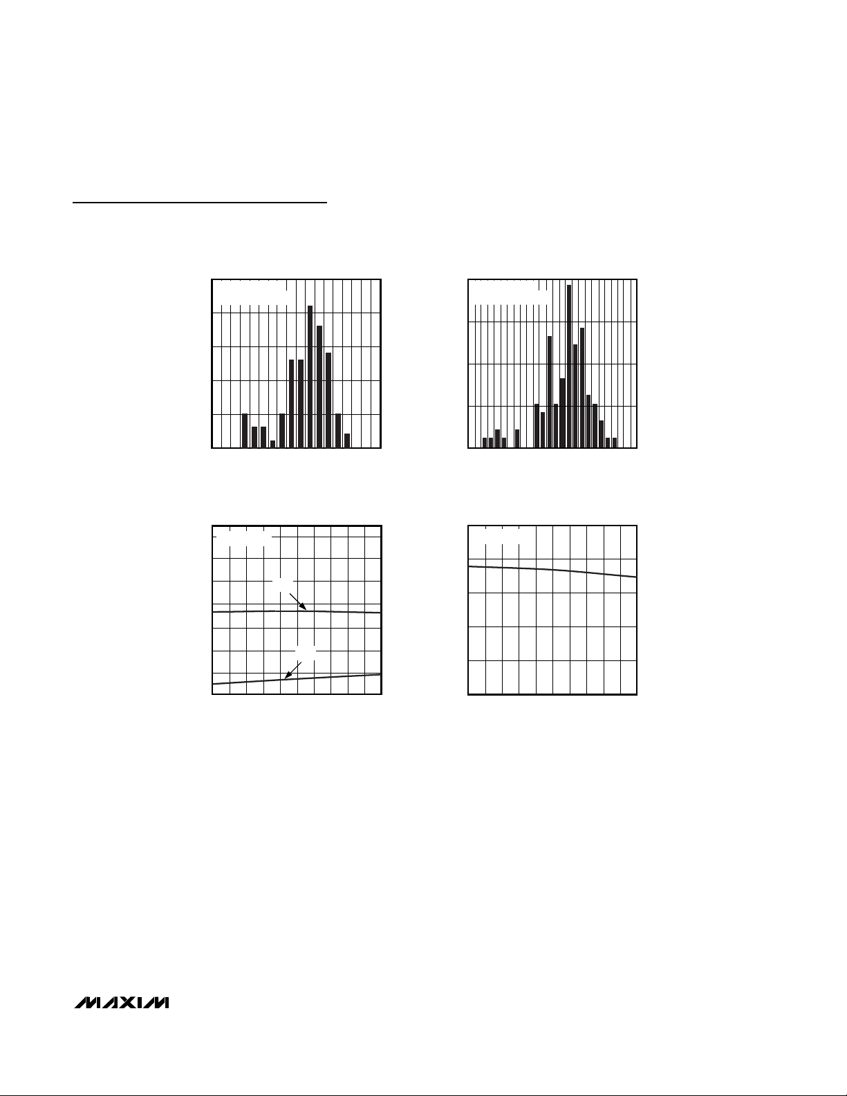
OUTPUT POWER HISTOGRAM AT FIXED
1.6V POWER DETECTOR VOLTAGE
MAX2242 toc09
OUTPUT POWER (dBm)
OCCURENCES
21.6 21.8 22 22.2 22.4
SIGMA = 0.14dBm
BASED ON
100 PARTS
Page 5
MAX2242
p2.4GHz to 2.5GHz
Linear Power Amplifier
_______________________________________________________________________________________ 5
Typical Operating Characteristics (continued)
(VCC= +3.3V, fIN= 2.45MHz, RF modulation = IEEE 802.11b, V
SHDN
= VCC, TA= +25°C, unless otherwise noted.)
0
5
15
10
20
25
OUTPUT POWER HISTOGRAM AT FIXED
0.8V POWER DETECTOR VOLTAGE
MAX2242 toc10
OUTPUT POWER (dBm)
OCCURRENCES
12.1 12.3 12.5 12.7 12.9 13.1 13.3 13.5 13.7
SIGMA = 0.25dBm
BASED ON 100 PARTS
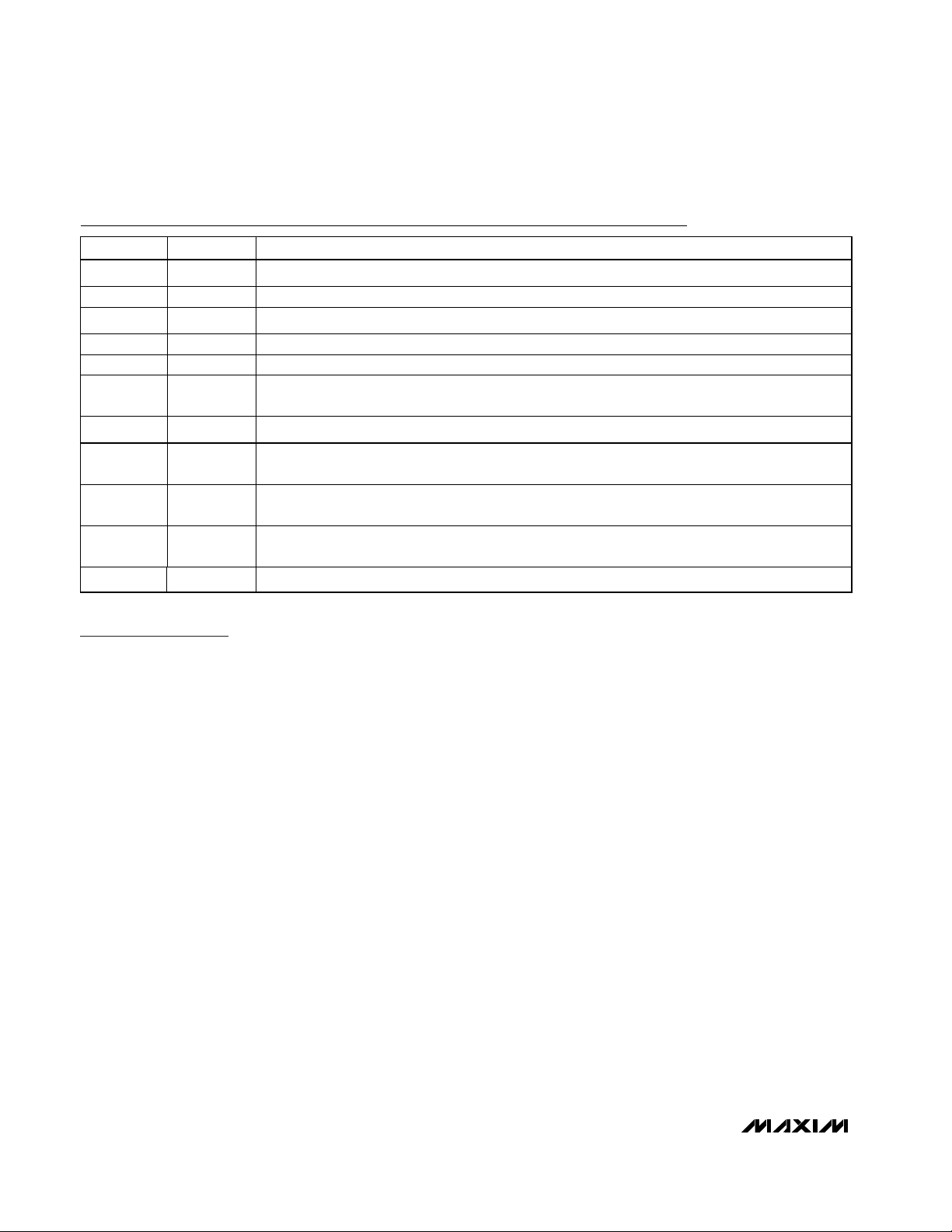
0
5
10
15
20
2.2 3.4 4.6 5.82.8 4.0 5.2 6.4 7.0
OUTPUT POWER HISTOGRAM AT FIXED
0.5V POWER DETECTOR VOLTAGE
MAX2242 toc11
OUTPUT POWER (dBm)
OCCURRENCES
SIGMA = 0.75dBm
BASED ON 100 PARTS
-13
-15
-11
-5
-3
-7
-9
-1
2400 2420 2440 2460 2480 2500
S11, S22, vs. FREQUENCY
MAX2242 toc12
FREQUENCY (MHz)
S11, S22 (dB)
PIN = -15dBm
S22
S11
25
26
27
28
29
30
2400 24402420 2460 2480 2500
MAX2242
S21 vs. FREQUENCY
MAX2242 toc13
FREQUENCY (MHz)
S21 (dB)
PIN = -15dBm
Page 6
Detailed Description
The MAX2242 is a linear PA intended for 2.4GHz ISMband wireless LAN applications. The PA is fully characterized in the 2.4GHz to 2.5GHz ISM band. The PA
consists of two driver stages and an output stage. The
MAX2242 also features an integrated power detector
and power shutdown control mode.
Dynamic Power Control
The MAX2242 is designed to provide optimum poweradded efficiency (PAE) in both high and low power
applications. For a +3.3V supply at high output power
level, the output power is typically +22.5dBm with an
idle current of 280mA. At low output-power levels, the
DC current can be reduced by an external DAC to
increase PAE while still maintaining sufficient ACPR
performance. This is achieved by using external resistors connected to the BIAS pin to set the bias currents
of the driver and output stages. The resistors are typically 8kΩ. Typically, a DAC voltage of 1.0V will give a
280mA bias current. Increasing the DAC voltage will
decrease the idle current. Similarly, decreasing the
DAC voltage will increase the idle current.
The BIAS pin is maintained at a constant voltage of
1.0V, allowing the user to set the desired idle current
using only two off-chip 1% resistors: a shunt resistor,
R2, from BIAS to ground; and a series resistor, R1, to
the DAC voltage, as shown in the Typical Application
Circuit. Resistor values R1 and R2 are determined as
follows:
V
MAX
= 1.0 + (1.0 ✕R1) / R2;
(I
CC
= 0, V
DAC
= V
MAX
) (1)
I
MAX
= (1.0 ✕1867) ✕(R1 + R2) / (R1 ✕R2);
(I
CC
= I
MAX
= max value, V
DAC
= 0) (2)
I
DAC
= (V
DAC
- 1.0) / R1 (3)
I
MID
= (1.0 ✕1867) / R2;
(V
DAC
= 1.0V or floating) (4)
I
CC
= 1867 ✕I
BIAS
(5)
where
V
MAX
= is the maximum DAC voltage
I
MAX
= is the maximum idle current
I
MID
= is the idle current with V
DAC
= 1.0V or not
connected
V
DAC
= is the DAC voltage
I
DAC
= is the DAC current
If no DAC is used and a constant idle current is
desired, use equation 4 to determine the resistor values
for a given total bias current. Only R2 is required.
MAX2242
2.4GHz to 2.5GHz
Linear Power Amplifier
6 _______________________________________________________________________________________
Pin Description
PIN NAME FUNCTION
A1 GND 3rd Stage Ground. Refer to Application Information section for detailed PC-board layout information.
A2 V
A3 GND 3rd Stage Ground. Refer to Application Information section for detailed PC-board layout information.
A4 V
B1 RF_OUT RF Output. Requires external matching.
B2 PD_OUT
B4 GND 1st Stage and Bias Control Circuit Ground
C1 BIAS
C2 SHDN
C3 V
C4 RF_IN RF Input. Requires external matching.
CC2
CC1
CCB
2nd Stage Supply Voltage. Bypass to ground using configuration in the typical operating circuit.
1st Stage Supply Voltage. Bypass to ground using configuration in the typical operating circuit.
Power Detector Output. This output is a DC voltage indicating the PA output power. Connect a
47kΩ resistor to GND.
Bias Control. Connect one 8kΩ resistor from BIAS to GND and one 8kΩ resistor from BIAS to DAC
block to set the idle current.
Shutdown Input. Drive logic low to place the device in shutdown mode. Drive logic high for normal
operation.
Bias Circuit DC Supply Voltage. Bypass to ground using configuration in the typical operating
circuit.
Page 7

MAX2242
2.4GHz to 2.5GHz
Linear Power Amplifier
_______________________________________________________________________________________ 7
For a DAC capable of both sourcing and sinking currents, the full voltage range of the DAC (typically from 0
to +3V) can be used. By substituting the desired values
of V
MAX
and I
MAX
into equations 1 and 2, R1 and R2
can be easily calculated.
For a DAC capable of sourcing current only, use equation 4 to determine the value of resistor R2 for the
desired maximum current. Use equation 1 to determine
the value of resistor R1 for the desired minimum current.
For a DAC capable of sinking current only, set resistors
R1 and R2 to 0 and connect the DAC directly to the
BIAS pin. Use equation 5 to determine the DAC current
required for a given ICC.
Shutdown Mode
Apply logic low to SHDN (pin C2) to place the
MAX2242 into shutdown mode. In this mode, all gain
stages are disabled and supply current typically drops
to 0.5µA. Note that the shutdown current is lowest when
V
SHDN
= 0.
Power Detector
The power detector generates a voltage proportional to
the output power by monitoring the output power using
an internal coupler. It is fully temperature compensated
and allows the user to set the bandwidth with an external capacitor. For maximum bandwidth, connect a
47kΩ resistor from PD_OUT to GND and do not use any
external capacitor.
Applications Information
Interstage Matching and Bypassing
V
CC1
and V
CC2
provide bias to the first and second
stage amplifiers, and are also part of the interstage
matching networks required to optimize performance
between the three amplifier stages. See the Typical
Application Circuit for the lumped and discrete component values used on the MAX2242 EV kit for optimum
interstage matching and RF bypassing. In addition to
RF bypass capacitors on each bias line, a global
bypass capacitor of 22µF is necessary to filter any
noise on the supply line. Route separate VCCbias
paths from the global bypass capacitor (star topology)
to avoid coupling between PA stages. Use the
MAX2242 EV kit PC board layout as a guide.
External Matching
The RFIN port requires a matching network. The RFIN
port impedance is 16–j30 at 2.45GHz. See the Typical
Application Circuit for recommended component values.
The RFOUT port is an open-collector output that must
be pulled to V
CC
through a 10nH RF choke for proper
biasing. A shunt 33pF capacitor to ground is required
at the supply side of the inductor. In addition, a matching network is required for optimum gain, efficiency,
ACPR, and output power. The load impedance seen at
the RFOUT port of the MAX2242 on the EV kit is
approximately 8 + j5Ω. This should serve as a good
starting point for your layout. However, optimum performance is layout dependent and some component optimization may be required. See the Typical Application
Circuit for the lumped and discrete component values
used on the MAX2242 EV kit to achieve this impedance.
Ground Vias
Placement and type of ground vias are important to
achieve optimum gain and output power and ACPR
performance. Each ground pin requires its own throughhole via (via diameter = 10mils) placed as near to the
device pin as possible to reduce ground inductance
and feedback between stages. Use the MAX2242 EV
kit PC board layout as a guide.
Layout and Thermal Management Issues
The MAX2242 EV kit serves as a layout guide. Use controlled-impedance lines on all high-frequency inputs
and outputs. The GND pins also serve as heat sinks.
Connect all GND pins directly to the topside RF ground.
On boards where the ground plane is not on the component side, connect all GND pins to the ground plane
with plated multiple throughholes close to the package.
PC board traces connecting the GND pins also serve
as heat sinks. Make sure that the traces are sufficiently
wide.
UCSP Reliability
UCSP represents a unique packaging form factor that
may not perform equally to a packaged product
through traditional mechanical reliability tests. UCSP
reliability is integrally linked to the user’s assembly
methods, circuit-board material, and usage environment. The user should closely review these areas when
considering use of a UCSP. Performance through the
operating-life test and moisture resistance remains
uncompromised as it is primarily determined by the
wafer-fabrication process. Mechanical stress performance is a greater consideration for a UCSP. UCSPs
are attached through direct solder contact to the user’s
PC board, foregoing the inherent stress relief of a packaged-product lead frame. Solder joint contact integrity
must be considered. Testing done to characterize the
Page 8

MAX2242
UCSP reliability performance shows that it is capable of
performing reliably through environmental stresses.
Users should also be aware that as with any interconnect system there are electromigration-based current
limits that, in this case, apply to the maximum allowable
current in the bumps. Reliability is a function of this current, the duty cycle, lifetime, and bump temperature.
See the Absolute Maximum Ratings section for any
specific limitations listed under Continuous Operating
Lifetime.Results of environmental stress tests and additional usage data and recommendations are detailed in
the UCSP application note, which can be found on
Maxim’s website at www.maxim-ic.com.
Chip Information
TRANSISTOR COUNT: 486
2.4GHz to 2.5GHz
Linear Power Amplifier
8 _______________________________________________________________________________________
Typical Application Circuit
Package Diagram
DAC
R1
8kΩ
BIAS
V
V
CCB
CC1
V
CC
33pF
V
CC
0.1µF
R2
8kΩ
0.1µF
SHDN
BIAS
CIRCUIT
V
CC
V
CC
DET
OUT
47kΩ
V
CC2
PD_OUT
DETECTOR
0.1µF
50Ω
33pF
10nH
100pF
RF_IN
2.2nH
NOTE: REFER TO MAX2242 EV KIT DATA SHEET FOR DETAILED LAYOUT INFORMATION.
6pF
GND
GND GND
1.8pF
RF_OUT
1.5
0.5
C4
C3
2.0
C2
0.5
C1
B4
B3
NOT
USED
B2
B1
A4
A3
A2
A1
0.75
MAX
BOTTOM VIEW
CHIP-SCALE PACKAGE (ALL DIMENSIONS IN mm)
SIDE VIEW
Page 9
Maxim cannot assume responsibility for use of any circuitry other than circuitry entirely embodied in a Maxim product. No circuit patent licenses are
implied. Maxim reserves the right to change the circuitry and specifications without notice at any time.
Maxim Integrated Products, 120 San Gabriel Drive, Sunnyvale, CA 94086 408-737-7600 _____________________ 9
© 2003 Maxim Integrated Products Printed USA is a registered trademark of Maxim Integrated Products.
2.4GHz to 2.5GHz
Linear Power Amplifier
Note: MAX2242 does not use bump B3.
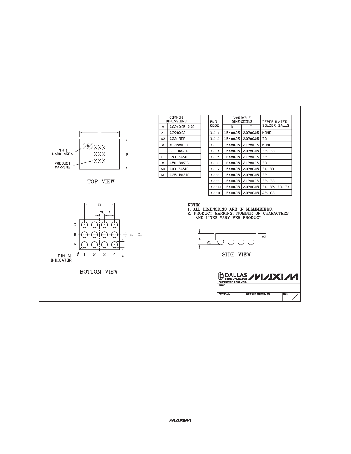
Package Information
(The package drawing(s) in this data sheet may not reflect the most current specifications. For the latest package outline information
go to www.maxim-ic.com/packages
.)
12L, UCSP 4x3.EPS
PACKAGE OUTLINE, 4x3 UCSP
21-0104
1
F
1
 Loading...