

Page 1
General Description
The MAX2240 single-supply, low-voltage power amplifier (PA) IC is designed specifically for applications in
the 2.4GHz to 2.5GHz frequency band. The PA is compliant with Bluetooth, HomeRF, and 802.11 standards,
as well as other FSK modulation systems. The PA provides a nominal +20dBm (100mW) output power in the
highest power mode.
The PA includes a digital power control circuit to greatly
simplify control of the output power. Four digitally controlled output power levels are provided: from +3dBm
to +20dBm. A digital input controls the active or shutdown operating modes of the PA. In the shutdown
mode, the current reduces to 0.5µA.
The IC integrates the RF input and interstage matching
to simplify application of the IC. Temperature and supply-independent biasing are also included to provide
stable performance under all operating conditions.
The IC operates from a +2.7V to +5V single-supply voltage. No negative bias voltage is required. Current consumption is a modest 105mA at the highest power
level.
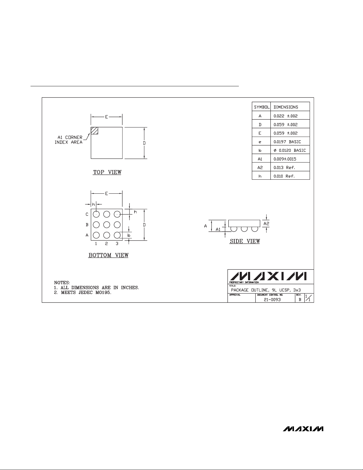
The part is packaged in the ultra-chipscale package
(UCSP), significantly reducing the required PC board
area. The chip occupies only a 1.56mm x 1.56mm area.
The 3 x 3 array of solder bumps are spaced with a
0.5mm bump pitch.
________________________Applications
Bluetooth
HomeRF
802.11 FHSS WLAN
2.4GHz ISM Proprietary Radios
Features
♦ 2.4GHz to 2.5GHz Frequency Range
♦ High +20dBm Output Power
♦ 2-Bit Digital Power Control: 4 Output Levels
♦ Integrated Input Match to 50Ω
♦ Low 105mA Operating Current
♦ 0.5µA Low-Power Shutdown Mode Current
♦ +2.7V to +5V Single-Supply Operation
♦ Ultra-Chipscale Package
(1.56mm x 1.56mm)
MAX2240
2.5GHz, +20dBm Power Amplifier IC
in UCSP Package
________________________________________________________________ Maxim Integrated Products 1
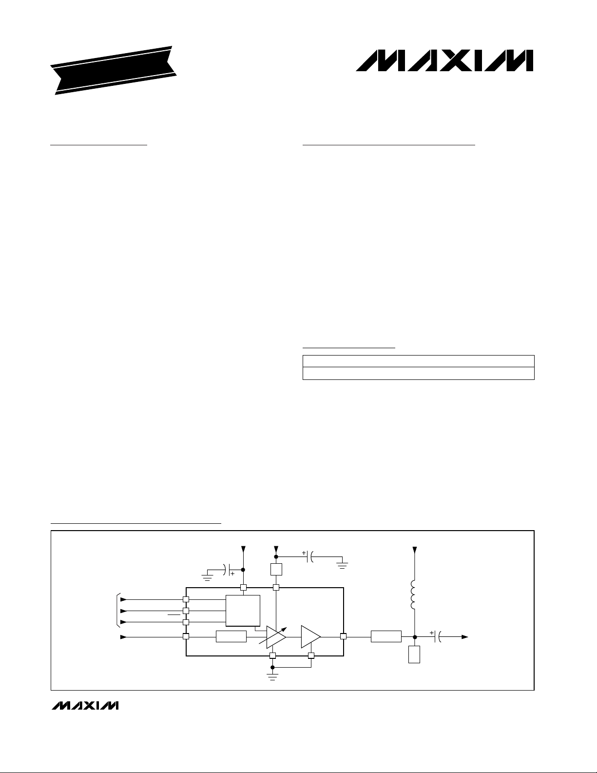
Typical Application Circuit/Functional Diagram
19-1624; Rev 0; 3/00
Ordering Information
9 UCSP*
PIN-PACKAGETEMP. RANGE
-40°C to +85°CMAX2240EBL
PART
*UCSP reliability is integrally linked to the user’s assembly
methods, circuit board material, and environment. Refer to the
UCSP Reliability Notice in the UCSP Reliability section of this
data sheet for more information.
Pin Configuration appears at end of data sheet.
For free samples and the latest literature, visit www.maxim-ic.com or phone 1-800-998-8800.
For small orders, phone 1-800-835-8769.
EVALUATION KIT MANUAL
FOLLOWS DATA SHEET
V
CC
220 pF
BIAS
D0
D1
LOGIC INPUTS
*INDUCTANCE CREATED WITH PC BOARD TRANSMISSION LINE
(SEE APPLICATIONS SECTION).
SHDN
RFIN
CONTROL
MATCH
BIAS &
POWER
V
CC
18pF
1.2nH* (BOARD TRACE)
V
CC
GND1 GND2
RFOUT
75Ω
θ = 26°
V
CC
65Ω
θ = 41°
22nH
RFOUT
10pF
Page 2
MAX2240
2.5GHz, +20dBm Power Amplifier IC
in UCSP Package
2 _______________________________________________________________________________________
ABSOLUTE MAXIMUM RATINGS
DC ELECTRICAL CHARACTERISTICS
(Using Typical Application Circuit, VCC= +2.7V to +5V, P
RFIN
= 0dBm to +4dBm, f
RFIN
= 2.4GHz to 2.5GHz, SHDN = VCC,
T
A
= -40°C to +85°C. Typical values measured at VCC= +3.2V, P
RFIN
= +3dBm, f
RFIN
= 2.45GHz, TA= +25°C, unless otherwise
noted.) (Note 1)
Stresses beyond those listed under “Absolute Maximum Ratings” may cause permanent damage to the device. These are stress ratings only, and functional
operation of the device at these or any other conditions beyond those indicated in the operational sections of the specifications is not implied. Exposure to
absolute maximum rating conditions for extended periods may affect device reliability.
BIAS, VCC, RFOUT to GND ......................................-0.3V to +6V
Input Voltages
(SHDN, D0, D1, to GND).......................-0.3V to (V
BIAS
+ 0.3V)
(RFIN to GND) ....................................................-0.7V to +0.7V
Input Current (SHDN, D0, D1) ..........................................±10mA
RF Input Power (RFIN)....................................................+10dBm
Continuous Power Dissipation (T
A
= +85°C)
9-Pin UCSP...................................................................810mW
Operating Temperature Range ...........................-40°C to +85°C
Storage Temperature Range .............................-65°C to +150°C
Supply Current
(Note 2)
Shutdown Supply Current
DIGITAL CONTROL INPUT (D0, D1, AND SHDN)
Input Logic Voltage High
Input Logic Voltage Low
Input Current GND ≤ VIN ≤ V
PARAMETER CONDITIONS MIN TYP MAX UNITS
VDI ≤ 0.8V, VDO ≤ 0.8V, TA = +25°C, P
V
= 3.2V, f
CC
VDI ≤ 0.8V, VDO ≤ 0.8V 110
VDI ≤ 0.8V, VDO ≥ 2.0V, TA = +25°C, P
V
= 3.2V, f
CC
VDI ≤ 0.8V, VDO ≥ 2.0V 111
V
≥ 2.0V, VDO ≤ 0.8V, TA = +25°C, P
DI
= 3.2V, f
V
CC
VDI ≥ 2.0V, VDO ≤ 0.8V 115
VDI ≥ 2.0V, VDO ≥ 2.0V, TA = +25°C, P
V
= 3.2V, f
CC
V
≥ 2.0V, VDO ≥ 2.0V 155
DI
SHDN ≤ 0.8V, VD0 ≤ 0.8V, VD1 ≤ 0.8V, no input signal 0.5 10.0
= 2.45GHz (Note 3)
RFIN
= 2.45GHz (Note 3)
RFIN
= 2.45GHz (Note 3)
RFIN
= 2.45GHz (Note 3)
RFIN
BIAS
RFIN
RFIN
RFIN
RFIN
= +3dBm,
= +3dBm,
= +3dBm,
= +3dBm,
65 80
68 85
75 90
105 125
2
11µA
0.8
mA
µA
V
V
Page 3
MAX2240
2.5GHz, +20dBm Power Amplifier IC
in UCSP Package
_______________________________________________________________________________________ 3
AC ELECTRICAL CHARACTERISTICS
(MAX2240 EV kit, VCC= +2.7V to +5V, P
RFIN
= 0dBm to +4dBm, f
RFIN
= 2.4GHz to 2.5GHz, SHDN = VCC, TA= +25°C. Typical values
measured at V
CC
= +3.2V, P
RFIN
= +3dBm, f
RFIN
= 2.45GHz, unless otherwise noted.)
All power levels set by D0, D1;
any load phase angle, any duration
All power levels set by D0, D1; load VSWR ≤ 3:1
SHDN = 1 to 0, D0 = D1 = logic high-to-low transition
CONDITIONS
6:1
Maximum Output VSWR Without
Damage (Note 8)
dB45
Input to Output Isolation in
Shutdown
dBm-30
Nonharmonic Spurious Output
(Note 9)
µs2
Power Ramp Turn-Off Time
(Notes 7, 9)
UNITSMIN TYP MAXPARAMETERS
VCC= 5.0V 268
Power Control Steps
(Notes 4, 9)
SHDN = 0 to 1, D0 = D1 = logic low-to-high transition
µs2
Power Ramp Turn-On Time
(Notes 6, 9)
dBm-15 -5Harmonic Output (Notes 3, 9)
RS= 50Ω, over full Pinrange dBm1.5:1 2:1
In-Band Spurious Noise
(Notes 5, 9)
Frequency offset = ±550kHz dBc-21 -20
Frequency offset = ±1.5MHz
dBm
-20
Frequency offset = ±2.5MHz -40
Input VSWR (Note 9)
VCC= 2.7V to 5.0V
dB
2 8.6
Note 1: Limits are 100% production tested at TA= +25°C. Limits over the entire operating temperature range are guaranteed by
design and characterization but are not production tested.
Note 2: Supply current is measured with RF power applied to the input.
Note 3: Measured with an output-matching network to minimize the 2nd and 3rd harmonics (see Applications section).
Note 4: Power steps between adjacent power levels. All other operating conditions remain constant during power step change.
Note 5: Output measured in 100kHz RBW. Test signal modulation shall comply with GFSK, BT = 0.5, 1-bit/symbol, 1Mbps, frequency
deviation = 175kHz.
Note 6: The total turn-on time for the PA output power to settle within 1dB of the final value.
Note 7: The total turn-off time for the PA output power to drop to -10dBm.
Note 8: After removal of the load mismatch, the PA returns to operation under normal conditions.
Note 9: Guaranteed by design and characterization.
MHz2400 2500Frequency Range
VD1≤ 0.8V, VD0≥ 2V 8
VD1≥ 2V, VD0≤ 0.8V 12
VD1≥ 2V, VD0≥ 2V, TA= -40°C to +85°C (Note 1) 15.3 19 24
VD1≤ 0.8V, VD0≤ 0.8V
dBm
3
Output Power
dBm04Input Power Range
Page 4

MAX2240
2.5GHz, +20dBm Power Amplifier IC
in UCSP Package
4 _______________________________________________________________________________________
)
)
Typical Operating Characteristics
(MAX2240 EV kit, VCC= +3.2V, P
RFIN
= +3dBm, f
RFIN
= 2.45GHz, SHDN = VCC, TA= +25°C, unless otherwise noted. See Table 1
for power level settings P1, P2, P3, P4.)
0
30
20
10
50
40
90
80
70
60
100
-40 -20 0 20 40 60 80 100
SHUTDOWN SUPPLY CURRENT
vs. TEMPERATURE
MAX2240 toc01
TEMPERATURE (°C)
SUPPLY CURRENT (nA)
SHDN = D0 = D1 = GND
V
CC
= 5.0V
V
CC
= 2.7V
V
CC
= 3.2V
2.5 3.53.0 4.0 4.5 5.0
MAX2240 toc02
SUPPLY VOLTAGE (V)
0
5
15
10
20
25
OUTPUT POWER (dBm)
OUTPUT POWER vs. SUPPLY VOLTAGE
P4
P3
P2
P1
20
0
40
80
60
100
120
2.5 3.53.0 4.0 4.5 5.0
MAX2240 toc08
SUPPLY VOLTAGE (V)
SUPPLY CURRENT (mA)
SUPPLY CURRENT vs. SUPPLY VOLTAGE
P4
P3
P2
P1
OUTPUT POWER vs. FREQUENCY
25
20
15
10
OUTPUT POWER (dBm)
5
0
2400 24402420 2460 2480 2500
FREQUENCY (MHz
OUTPUT POWER vs. INPUT POWER
25
20
P4
15
P3
10
5
P2
0
OUTPUT POWER (dBm)
-5
P1
-10
-15
-5 -1-3 1 3 5
INPUT POWER (dBm)
OUTPUT POWER vs. TEMPERATURE
25
P4
MAX2240 toc05
P3
P2
P1
20
15
10
OUTPUT POWER (dBm)
5
0
-40
0-20 20 40 60 80
TEMPERATURE (°C
OUTPUT POWER vs. PINC2 VOLTAGE
25
20
MAX2240 toc07
15
10
5
0
-5
OUTPUT POWER (dBm)
-10
-15
-20
1.0 2.01.5 2.5 3.0 3.5
V
PINC2
(V)
MAX2240 toc06
P4
P3
P2
P1
SUPPLY CURRENT vs. INPUT POWER
120
P4
P3
P2
P1
110
MAX2240 toc04
100
SUPPLY CURRENT (mA)
90
80
70
60
50
40
021345
INPUT POWER (dBm)
P4
MAX2240 toc08
P3
P2
P1
FSK MODULATED OUTPUT SPECTRUM
30
20
10
0
-10
-20
-30
OUTPUT POWER (dBm)
-40
-50
PEAK DEV = ±175kHz
BT = 0.5
-60
1Msps
-70
CENTER = 2.45GHz
SPAN = 5MHz
MAX2240 toc09
Page 5

MAX2240
2.5GHz, +20dBm Power Amplifier IC
in UCSP Package
_______________________________________________________________________________________ 5
NAME FUNCTION
C3 RFIN Power Amplifier RF Input. Internally DC blocked and matched to 50Ω.
C2 V
CC
DC Voltage Supply for 1st Stage. A 1.2nH series inductance required for optimum output power and efficiency, followed by an external RF bypass capacitor to ground.
PIN
C1 GND2
Ground Connection to the Amplifier 2nd Stage. Requires a low-inductance/low thermal resistance path to
the ground plane with multiple vias.
B3 GND1
Ground Connection for Bias and 1st Stage. Requires a low-inductance/low thermal resistance path to the
ground plane with multiple vias.
A2 D1 Digital Power Control Input (MSB) (Table 1)
A3 BIAS
DC Voltage Supply for Bias and Control Circuitry. An external RF bypass capacitor to ground is required.
Place capacitor as close to the pin as possible.
B1 RFOUT
Power Amplifier RF Output. Open-collector output requires external pull-up inductor to VCC. Requires an
external matching network for optimum output power and efficiency.
B2
SHDN
Power Amplifier Shutdown Control Input. Drive SHDN low to enable low-power shutdown mode. Drive SHDN
high for normal operation.
A1 D0 Digital Power Control Input (LSB) (Table 1)
Pin Description
MAX2240 toc10
HARMONIC OUTPUT SPECTRUM
f
0
2f
0
5f
0
3f
0
4f
0
START = 1.0GHz
STOP = 13.0GHz
-70
-30
-40
-50
-60
0
-10
-20
30
20
10
OUTPUT POWER (dBm)
MAX2240 toc11
S
11
START = 2400MHz
STOP = 2500MHz
MAX2240 toc12
POWER-ON/OFF CHARACTERISTICS
-70
-60
-50
-40
-10
0
10
-30
-20
20
30
200ns/div
OUTPUT POWER (dBm)
Typical Operating Characteristics (continued)
(MAX2240 EV kit, VCC= +3.2V, P
RFIN
= +3dBm, f
RFIN
= 2.45GHz, SHDN = VCC, TA= +25°C, unless otherwise noted. See Table 1
for power level settings P1, P2, P3, P4.)
_______________Detailed Description
The MAX2240 PA is guaranteed to operate over a
2.4GHz to 2.5GHz frequency range with a +2.7V to
+5V single supply. The PA provides a nominal +20dBm
output power in the highest power mode setting (D0 =
D1 = 1). The signal path consists of two amplifier
stages: an input amplifier stage and a PA stage. A
matching circuit is provided between the two stages to
match the amplifiers’ impedance. The PA also contains
bias circuits that interface to external logic commands
(D0, D1, and SHDN) to control output power and
power-up/down of the amplifier.
The input amplifier is an AC-coupled variable gain
amplifier (VGA) with its input port internally matched to
50Ω. The amplifier is AC-coupled; hence, a DC blocking capacitor is not required at the RFIN port. The VGA
gain is varied by changing the bias current through a
current driver circuit. The current driver circuit provides
Page 6

four levels (magnitudes) of precisely controlled currents
to the VGA, depending on power control digital inputs
D0 and D1. Each current level presents a different
power level to the final amplifier stage, therefore controlling the output power.
The digital power control circuit of the PA greatly simplifies control of the output power. The two digital bits
D0 and D1 control the output power in four steps with
approximately a 6dB/step. The PA is optimized to provide power control steps within a 2dB/step to 8.6dB/
step over the full temperature range and VCCand RF
input power variations. Table 1 shows the D0 and D1
digital control states, the corresponding nominal output
power, and the typical current consumption of the IC.
The bias circuit provides separate bias voltages and
currents to the amplifier stages. An internal lowpass RC
filter isolates the bias circuit from being corrupted by
the RF signals. The bias circuit is optimized to minimize
output power variations due to the variations in temperature, VCC, and RF power input. The bias circuit design
also ensures the stability of the PA when connected to
high VSWR loads over all power levels. A digital low at
the SHDN port turns the amplifier down with a current
consumption of less than 1µA.
The MAX2240 integrates all the RF matching components on-chip, except for the output stage match. The
internal input match enables the RF input with 50Ω
impedance to be directly connected to the RFIN port
through a 50Ω transmission line.
The MAX2240 PA requires an external match at the
RFOUT port to optimize the amplifier for output power
and efficiency. For an optimum match at 2.45GHz, the
load impedance at the RFOUT port is approximately
15Ω + j18Ω (Figure 1). There are numerous ways of
transforming 50Ω to the optimum impedance. The output matching in the typical operating circuit is implemented using a series transmission line of 75Ω and
electrical length of 26°, and an open-ended shunt stub
of 65Ω and 41° in length. The shunt stub also reduces
the second harmonic at the output.
Applications Information
The MAX2240 power amplifier requires a relatively
small number of external components. These components are small, low-cost surface-mount passive elements. The capacitors are all 0402 multilayer ceramic
chip capacitors. These capacitors possess excellent
high-frequency properties and are cost effective. The
Typical Application Circuit is shown on page 1.
The inductor is a Q (>25) 0603 chip inductor. All transmission lines are simple microstrip structures printed
on the PC board.
Power-Supply Considerations
The MAX2240 is designed to operate from a single, positive supply voltage (V
CC
). Three pins are fed by the supply voltage: BIAS, VCC, and RFOUT. Each supply
voltage connection requires a separate RF bypass
capacitor for proper operation. Use a 0.1µF bypass
capacitor to filter the supply at the common VCCnode
(see Typical Application Circuit).
BIAS requires a 220pF capacitor to ground. Locate one
end of the capacitor as close as possible to BIAS and
the other end of the capacitor near GND1 with several
vias to the ground plane.
V
CC
powers the amplifier 1st stage output. A 1.2nH
inductor in series with VCCand the VCCbypass capacitor is needed for optimal output power and efficiency.
An 18pF bypass capacitor to ground is required at the
supply end of the 1.2nH inductor.
RFOUT is connected to the power supply through a
choke inductor (through transmission line section T1).
Select a choke with a self-resonant frequency at or
slightly below 2.4GHz. A 220pF bypass capacitor is
needed at the supply voltage end of the inductor.
MAX2240
2.5GHz, +20dBm Power Amplifier IC
in UCSP Package
6 _______________________________________________________________________________________
P3
P2
P1
PA OFF-
POWER LEVEL
OUTPUT POWER AND SUPPLY CURRENT
7531
6831
6531
<1µA30
I
CC
(mA)
P
IN
(dBm)
SHDN
DIGITAL CONTROL INPUTS
12
8
3
-22
P
OUT
(dBm)
1
0
0
0
D1
0
1
0
0
D0
191 P41 10531
Table 1. Control Inputs
Page 7

RF Input
The internal input stage impedance matching network
is integrated on the MAX2240, so it is possible to
directly connect a 50Ω transmission line to RFIN. No
external matching is required.
Output Stage (RF Output)
The output stage of the MAX2240 power amplifier is the
collector of a transistor. The DC bias and impedance
matching network are off-chip as shown in the Typical
Application Circuit.
An off-chip external network, as with most PA ICs, is
used to achieve higher efficiency and output power
than is typically achieved using low-Q on-chip matching elements. Optimum output power and efficiency are
achieved with a particular impedance on the output at
the operating frequencies of interest and a “short” at
the RF harmonic frequencies. This impedance is specified relative to a reference plane at the amplifier output
into the matching network and load. This is the impedance that achieves the output power and current consumption listed in the electrical specifications. It is
shown below in the chart and table of Figure 1.
The primary power-matching structure is a lowpass network formed by the series transmission line section T1
and the open-stub transmission line section T2. The
transmission line network acts like a series inductance
and shunt capacitance. T1 and T2 are expressed as
electrical lengths of a particular characteristic impedance line, but could be designed with different impedance lines.
Choose the length of T2 to provide a “short” at the 2nd
harmonic frequency of the fundamental, and significantly
attenuate its amplitude at the output—1/4 wave at the
2nd harmonic frequency of 4.9GHz. The 3rd harmonic is
attenuated through the clever use of the parasitic capacitance in the choke. This capacitance rolls off the choke
impedance at higher frequencies and appears as a
low impedance at the 3rd harmonic frequency.
The output series capacitor is used as a DC blocking
capacitor and a final matching element. A value of
10pF is recommended.
As explained in the Power-Supply Considerations section, for proper DC biasing, the PA requires a connection
to VCCthrough an inductor, serving as a choke. Locate
the inductor on the load side of transmission line T1. The
recommended inductor value is 22nH. However, its
value is not critical but must provide an impedance that
is several hundred ohms. Choose an inductor with a selfresonant frequency at or slightly below 2.4GHz. The
inductor Q is not critical; a moderate Q (>25) is sufficient. Remember to provide sufficient current-handling
capability for the inductor, in this case at least 200mA.
Also, a 220pF bypass capacitor is recommended at the
supply voltage end of the inductor.
Layout
Design the layout for the PA IC to be as compact as
possible to minimize the magnitude of parasitics. The
chipscale IC package uses a bump pitch of 0.5mm
(19.7mil) and bump diameter of 0.3mm (~12mil).
Therefore, lay out the solder pad spacing on 0.5mm
(19.7mil) centers, use a pad size of 0.25mm (~10mil)
and a solder mask opening of 0.33mm (13mil). Round or
square pads are permissible. (Refer to the Maxim document, Wafer Level Ultra-Chipscale Packaging for additional detailed information on UCSP layout and handling.)
Connect multiple vias from the ground plane as close to
the ground pins as possible.
As already described, locate the capacitors as close as
possible to the IC supply voltage pin or supply end of
the series inductor. Place the ground end of these
capacitors near the IC GND pins to provide a lowimpedance return path for the signal current.
MAX2240
2.5GHz, +20dBm Power Amplifier IC
in UCSP Package
_______________________________________________________________________________________ 7
0.59
0.57
2.5
2.45
2.4
FREQUENCY
(GHz)
13615.0
13815.2
14015.5
<Γ| Γ |
R X
19.0
17.9
16.7
Figure 1. Output Impedance
0.58
MATCHING IMPEDANCE
SMITH CHART
MATCHING IMPEDANCE FOR RF
2
1
OUT
PIN
1: (15.5Ω + J16.7Ω), 2.4GHz
2: (15.0Ω + 19.0Ω), 2.5GHz
Page 8
MAX2240
2.5GHz, +20dBm Power Amplifier IC
in UCSP Package
8 ____________________________________________________________________________________________________
SHDN
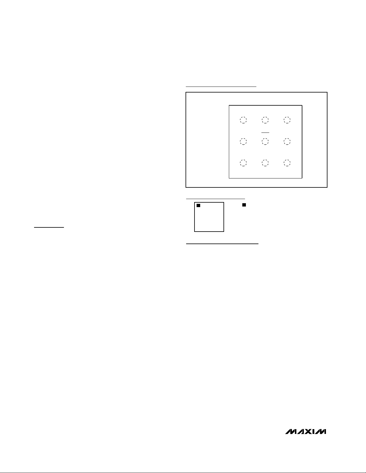
SHDN is located in the center of the bump layout of the
MAX2240. Therefore, the SHDN line requires the use of
either a via to a buried line or a trace that fits inside a
10mil gap between solder pads to bring out a connection from SHDN.
D0, D1 Pins
Digital power control inputs D0 and D1 have CMOSlogic level inputs. As in any PC board circuit, the length
of the logic signal traces determines the susceptibility
to high-frequency noise that may interfere with normal
switching. Therefore, in some cases it may be necessary to provide some local lowpass filtering of the logic
traces to suppress HF noise coupling to these inputs.
Output Match Layout
It is possible to lay out the output matching network
transmission traces in a more compact manner if PC
board area is limited. Series lines T1 and T2 may be
constructed as folded lines, though it may be necessary to chamfer the corners for wide lines.
Prototype Chip Installation
Alignment keys on the PC board around the area where
the chip is located will be helpful in the prototype
assembly process. The MAX2240 EV kit PC board has Lshaped alignment keys at the diagonal corners of the
chip. It is better to align the chip on the board before any
other components are placed, and then place the board
on a hotplate or hot surface until the solder starts melting. Remove the board from the hotplate without disturbing the position of the chip, and let it cool down to room
temperature before processing the board further.
Marking Information
: Pin 1 ID
AAA: Product ID code
XXX: Lot Code
Chip Information
TRANSISTOR COUNT: 771
AAA
XXX
Pin Configuration
TOP VIEW
(BUMPS AT THE
BOTTOM)
A
B
C
1
DO DI BIAS
A1
RFOUT SHDN GND1
B1
GND2 V
C1
2
A2
B2
CC
C2
UCSP
3
A3
B3
RFIN
C3
Page 9
MAX2240
2.5GHz, +20dBm Power Amplifier IC
in UCSP Package
_______________________________________________________________________________________ 9
Table 2. Reliability Test Data
UCSP Reliability
The ultra-chipscale package (UCSP) represents a unique
packaging form factor that may not perform equally to a
packaged product through traditional mechanical reliability tests. CSP reliability is integrally linked to the user’s
assembly methods, circuit board material, and usage
environment. The user should closely review these areas
when considering use of a CSP package. Performance
through Operating Life Test and Moisture Resistance
remains uncompromised as it is primarily determined by
the wafer-fabrication process.
Mechanical stress performance is a greater consideration for a CSP package. CSPs are attached through
direct solder contact to the user’s PC board, foregoing
the inherent stress relief of a packaged product lead
frame. Solder joint contact integrity must be considered.
Table 2 shows the testing done to characterize the CSP
reliability performance. In conclusion, the UCSP is capable of performing reliably through environmental stresses
as indicated by the results in the table. Additional usage
data and recommendations are detailed in the UCSP
application note, which can be found on Maxim’s website at www.maxim-ic.com.
TEST CONDITIONS DURATION
Temperature Cycle
Operating Life TA = +70°C 240hr 0/10
Moisture Resistance +20°C to +60°C, 90% RH 240hr 0/10
Low-Temperature Storage -20°C 240hr 0/10
Low-Temperature
Operational
Solderability 8hr steam age — 0/15
ESD ±2000V, Human Body Model — 0/5
High-Temperature Operating
Life
-35°C to +85°C,
-40°C to +100°C
-10°C 24hr 0/10
= +150°C 168hr 0/45
T
J
150 cycles,
900 cycles
NO. OF FAILURES PER
SAMPLE SIZE
0/10,
0/200
Page 10
MAX2240
2.5GHz, +20dBm Power Amplifier IC
in UCSP Package
10 ______________________________________________________________________________________
Package Information
9LUCSP, 3x3.EPS
 Loading...