

Page 1
General Description
The MAX2235 low-voltage, silicon RF power amplifier
(PA) is designed for use in the 900MHz frequency band.
It operates directly from a single +2.7V to +5.5V supply,
making it suitable for use with 3-cell NiCd or 1-cell Li-Ion
batteries. The device delivers +30dBm (1W) typical output power from a +3.6V supply or +28dBm from a +2.7V
supply.
The MAX2235’s gain is adjustable over a 37dB range.
A power-control pin controls gain and bias to maintain
optimum efficiency, even at lower output power levels,
thus extending the operating life of the battery. At
+30dBm output power, efficiency is typically 47%. An
additional power-saving feature is a shutdown mode
that typically reduces supply current below 1µA.
A key feature of this PA is its autoramping capability.
During turn-on and turn-off periods, the RF envelope is
controlled to approximate a raised cosine on the rising
and falling edge, thereby minimizing transient noise
and spectral splatter. The ramp time is set by selecting
the value of an external capacitor.
The MAX2235 is intended for use in constant envelope
applications such as AMPS, two-way paging, or FSKbased communications in the 900MHz ISM band. The
device is available in a thermally enhanced 20-pin
TSSOP package with a heat slug.
Applications
900MHz ISM-Band Applications
Two-Way Pagers
Analog Cellular Phones
Microcellular GSM (Power Class 5)
Wireless Data Networks
Features
♦ 800MHz to 1000MHz Operation
♦ High Output Power at 836MHz
+32.5dBm at +5.0V
+30dBm at +3.6V
+29dBm at +3.0V
+28dBm at +2.7V
♦ +2.7V to +5.5V Single-Supply Operation
♦ Automatic Power-Up/Power-Down Ramp
♦ Direct On/Off Keying (OOK) without Intersymbol
Interference or VCO Pulling
♦ 37dB Power-Control Range
♦ 47% Efficiency
♦ <1µA Supply Current in Shutdown Mode
♦ Small 20-Pin TSSOP Package with Heat Slug
MAX2235
+3.6V, 1W Autoramping Power
Amplifier for 900MHz Applications
________________________________________________________________ Maxim Integrated Products 1
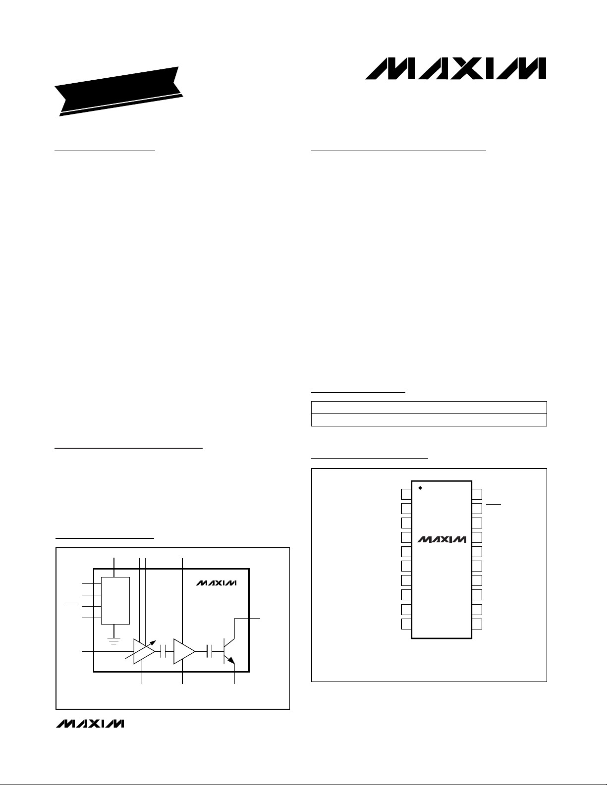
Functional Diagram
19-1463; Rev 2; 10/00
PART
MAX2235EUP -40°C to +85°C
TEMP. RANGE PIN-PACKAGE
20 TSSOP-EP
EVALUATION KIT
AVAILABLE
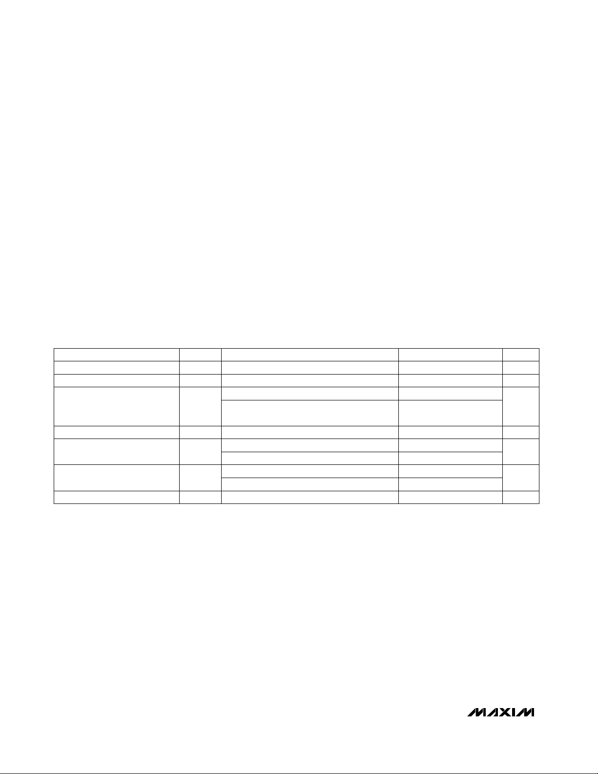
Pin Configuration
Ordering Information
For pricing, delivery, and ordering information, please contact Maxim/Dallas Direct! at
1-888-629-4642, or visit Maxim’s website at www.maxim-ic.com.
V
CCVCCVCC
4 3 5 8, 9
11
RAMP
12
REF
SHDN
GC
RFIN
NOTE: SOLDER UNDERSIDE OF METAL SLUG TO BOARD GND PLANE.
BIAS
19
20
1
VGA
V
CC
MAX2235
6, 7, 102
RFOUT
15, 16
13, 14, 17, 18, SLUG
GNDGND GND
TOP VIEW
1
RFIN
2
GND
3
V
CC
4
CC
5
6
7
8
9
10
MAX2235
TSSOP-EP
V
CC
GND
GND
CC
V
CC
NOTE: THE GROUND OF THE OUTPUT STAGE IS CONNECTED TO THE
UNDERSIDE METAL SLUG.
20
GC
19
SHDN
18
GND
17
GNDV
16
RFOUT
15
RFOUT
14
GND
13
GNDV
12
REF
11
RAMPGND
Page 2
MAX2235
+3.6V, 1W Autoramping Power
Amplifier for 900MHz Applications
2 _______________________________________________________________________________________
ABSOLUTE MAXIMUM RATINGS
DC ELECTRICAL CHARACTERISTICS
(VCC= +2.7V to +5.5V, GC = RAMP = REF = unconnected, no input signal applied, TA= -40°C to +85°C, unless otherwise noted.
Typical values are at V
CC
= +3.6V and TA= +25°C.)
Stresses beyond those listed under “Absolute Maximum Ratings” may cause permanent damage to the device. These are stress ratings only, and functional
operation of the device at these or any other conditions beyond those indicated in the operational sections of the specifications is not implied. Exposure to
absolute maximum rating conditions for extended periods may affect device reliability.
VCCto GND...........................................................-0.3V to +6.5V
SHDN to GND.............................................-0.3V to (V
CC
+ 0.3V)
GC to GND .................................................-0.3V to (V
CC
+ 0.3V)
RF Input Power .................................................+13dBm (20mW)
Maximum Load Mismatch without Damage,
V
CC
= +2.7V to +3.4V, Any Load Phase Angle,
Any Duration.......................................................................20:1
Maximum Load Mismatch without Damage,
V
CC
= +3.4V to +5.5V, Any Load Phase Angle,
Any Duration.........................................................................8:1
Continuous Power Dissipation (T
A
= +70°C)
TSSOP (derate 80mW/°C above T
A
= +70°C) ..................6.4W
Operating Temperature Range ...........................-40°C to +85°C
Junction Temperature......................................................+150°C
Storage Temperature Range .............................-65°C to +150°C
Lead Temperature (soldering, 10s) .................................+300°C
SHDN = GND
(Note 1)
(Note 2)
V
SHDN
> 2.3V, VGC> 0.6V
V
SHDN
< 0.5V, VGC< 0.4V
2.7V < VCC< 3.4V, SHDN = GND,
T
A
= +55°C
V
SHDN
= 2.0V
V
SHDN
< 0.5V
CONDITIONS
0.5 100
V0.5V
IL
V2.0V
IH
SHDN Logic High
SHDN Logic Low
V2.0 2.2 2.4V
GCNOM
GC Open-Circuit Voltage
µA
-10 1.0
I
GC
GC Input Current
-0.5 0.5
I
SHDN
Shutdown Supply Current µA
2
0.5
µA
-0.5 0.5
I
INSHDN
SHDN Input Current
UNITSMIN TYP MAXSYMBOLPARAMETER
VGC< 0.4 mA20I
STBY
Standby Supply Current
Page 3
MAX2235
+3.6V, 1W Autoramping Power
Amplifier for 900MHz Applications
_______________________________________________________________________________________ 3
Note 1: ≥ +25°C guaranteed by production test, <+25°C guaranteed by design and characterization.
Note 2: MAX guaranteed by production test, MIN guaranteed by design and characterization.
Note 3: Guaranteed by design and characterization.
Note 4: For optimum performance at a given frequency, design the output matching network for maximum output power.
Note 5: Gain is monotonic with V
GC
.
Note 6: 0.068µF capacitor from RAMP to REF. Time is measured from SHDN low-to-high transition to +29dBm output power, or
from SHDN high-to-low transition to -25dBm output power.
Note 7: Harmonics measured on the evaluation kit, which provides some harmonic attenuation in addition to the rejection provided
by the IC. The combined suppression is specified.
P
RFIN
adjusted to give P
RFOUT
= +24dBm
P
RFOUT
= +30dBm
P
RFIN
= 0dBm, VGCadjusted to give
P
RFOUT
= 24dBm
315
610
Average Supply Current
%47PAEPower Added Efficiency
0.6V < VGC< 2.3V dB37
dB24 26G
P
Power Gain
Gain-Control Range (Note 5)
mW/µs1.6dP/dt
Auto-Power Ramping-Up
Maximum Slope (Note 6)
Input VSWR relative to input impedance in
operating mode
VCC= 2.7V to 5.5V, 6:1 VSWR at any phase
angle
1.5:1∆VSWR
Standby Mode Input VSWR
Change
50Ω source impedance
dBc-60
Maximum Nonharmonic
Spurious Output Due to Load
Mismatch
1.5:1VSWRInput VSWR
mW/µs-1.3dP/dt
Auto-Power Ramping-Down
Minimum Slope (Note 6)
30kHz BW at offset = 45MHz dBm-90Noise Power
40 48
P
RFIN
= +7dBm dBc30 38Harmonic Suppression (Note 7)
mA
305
I
CC
P
RFIN
= 0dBm dB
25 36
Off-Isolation
V
SHDN
= 0.5V
GC = GND
AC ELECTRICAL CHARACTERISTICS
(MAX2235 Evaluation Kit, GC = unconnected, P
RFIN
adjusted to give P
RFOUT
= +30dBm, f
RFIN
= 836MHz, VCC= V
SHDN
= +3.6V,
T
A
= +25°C, unless otherwise noted.) (Note 3)
CONDITIONS UNITSMIN TYP MAXSYMBOLPARAMETER
VCC= 2.7V 28.0
VCC= 3.0V, TA= T
MIN
to T
MAX
25.5
VCC= 3.0V (Note 4)
27.0 28.7
VCC= 3.6V
30.3
VCC= 5.0V
dBm
32.5
P
RFOUT
Minimum Output Power
MHz
800 1000
f
RFIN
Operational Frequency Range
(Note 4)
Page 4
MAX2235
+3.6V, 1W Autoramping Power
Amplifier for 900MHz Applications
4 _______________________________________________________________________________________
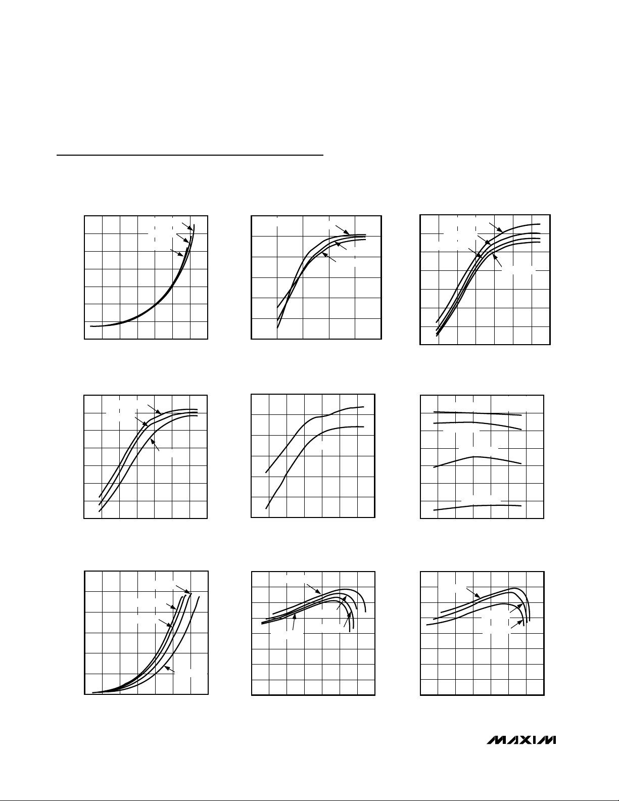
Typical Operating Characteristics
(MAX2235 Evaluation Kit, GC = unconnected, f
RFIN
= 836MHz, VCC= V
SHDN
= +3.6V, TA= +25°C, unless otherwise noted.)
0
200
100
400
300
600
500
700
010155 20253035
SUPPLY CURRENT vs. OUTPUT POWER
MAX2235 toc01
OUTPUT POWER (dBm)
I
CC
(mA)
TA = -40°C
TA = +25°C
TA = +85°C
-20
0
-10
20
10
30
40
0 1.00.5 1.5 2.0 2.5
OUTPUT POWER
vs. VOLTAGE AT GC PIN
MAX2235 toc02
VGC (V)
OUTPUT POWER (dBm)
P
RFIN
= 0dBm
TA = -40°C
TA = +25°C
TA = +85°C
0
10
5
20
15
30
25
35
-25 -15 -10-20 -5 0 5 10
OUTPUT POWER vs. INPUT POWER
MAX2235 toc03
INPUT POWER (dBm)
OUTPUT POWER (dBm)
VCC = +5.0V
VCC = +3.6V
VCC = +3.0V
VCC = +2.7V
0
10
5
20
15
30
25
35
-25 -15 -10-20 -5 0 5 10
OUTPUT POWER vs. INPUT POWER
AND TEMPERATURE
MAX2235 toc04
INPUT POWER (dBm)
OUTPUT POWER (dBm)
TA = -40°C
TA = +25°C
TA = +85°C
0
20
10
40
30
50
60
015205 10 253035
EFFICIENCY vs. OUTPUT POWER
MAX2235 toc07
OUTPUT POWER (dBm)
EFFICIENCY (%)
VCC = +5.0V
VCC = +3.6V
VCC = +3.0V
VCC = +2.7V
-60
-40
-50
-20
-30
-10
0
-25 -10 -5-20 -15 0 5 10
SECOND AND THIRD HARMONICS
vs. INPUT POWER
MAX2235 toc05
INPUT POWER (dBm)
HARMONIC POWER (dBm)
2nd
3rd
0
10
5
20
15
30
25
35
820 830 835825 840 845 850 855
OUTPUT POWER vs. FREQUENCY
MAX2235 toc06
INPUT FREQUENCY (MHz)
OUTPUT POWER (dBm)
P
RFIN
= +3dBm
P
RFIN
= -5dBm
P
RFIN
= -13dBm
P
RFIN
= -21dBm
MATCHED AT
836MHz
0
10
5
20
15
30
25
35
010155 20253035
POWER GAIN vs. OUTPUT POWER
MAX2235 toc08
OUTPUT POWER (dBm)
POWER GAIN (dB)
VCC = +5.0V
VCC = +3.6V
VCC = +3.0V
40
VCC = +2.7V
0
10
5
20
15
35
30
25
40
0105 1520253035
POWER GAIN vs. OUTPUT POWER
AND TEMPERATURE
MAX2235 toc09
OUTPUT POWER (dBm)
POWER GAIN (dB)
TA = -40°C
TA = +25°C
TA = +85°C
Page 5

MAX2235
+3.6V, 1W Autoramping Power
Amplifier for 900MHz Applications
_______________________________________________________________________________________ 5
Typical Operating Characteristics (continued)
(MAX2235 Evaluation Kit, GC = unconnected, f
RFIN
= 836MHz, VCC= V
SHDN
= +3.6V, TA= +25°C, unless otherwise noted.)
0
400
200
800
600
1000
1200
0406020 80 100 120
FALL TIME vs. RAMPING CAPACITANCE
MAX2235 toc11
CAPACITANCE (nF)
FALL TIME (µs)
FULL POWER = +20dBm
FULL POWER = +10dBm
FULL POWER = +30dBm
NAME FUNCTION
1 RFIN
RF Input. A DC blocking capacitor in series with RFIN is required. The value of the capacitor depends on
the operating frequency.
PIN
Pin Description
2 GND
GND connection for the input stage (variable-gain amplifier). Connect to the circuit board ground plane
with a separate low-inductance path (via).
3 V
CC
Supply Voltage Input for the Input Stage. Bypass with its own 100pF low-inductance capacitor to GND.
4 V
CC
Supply Voltage Input for Bias Circuitry. Bypass with its own 100pF low-inductance capacitor and a 1000pF
capacitor to GND, to minimize RF signal coupling into the bias circuits.
5 V
CC
Supply Voltage Input for the Input Stage. Bypass with its own 22pF low-inductance capacitor to pins 6 and 7.
6, 7, 10 GND
GND Connection for the Second-Stage Amplifier (driver). Connect to the circuit board ground plane with a
separate low-inductance path (via).
8 V
CC
Supply Voltage Input for the Second Stage. Bypass with its own 220pF and 1000pF low-inductance
capacitors to GND.
9 V
CC
Supply Voltage Input for the Second Stage. Connect to pin 8.
11 RAMP
Power Ramp Pin. Connect a capacitor between RAMP and REF to provide a gradual linear power-up/down
ramp. See Detailed Description.
12 REF Reference Voltage for RAMP Capacitor. The reference is internally set to 1.9V.
13, 14,
17, 18,
SLUG
GND
GND Connection for the Power Stage. Solder the slug to the circuit board ground plane. Connect pins 13,
14, 17, and 18 to the slug with a straight board trace under the chip.
15 RFOUT
Power Amplifier Output. See Typical Operating Circuit for an example of a matching network, which provides optimal output power at 836MHz. Connect to pin 16.
16 RFOUT Power Amplifier Output. Connect to pin 15.
19
SHDN
Shutdown Pin. Drive SHDN low to turn the device off. Drive above 2.0V to turn the device on. Drive V
SHDN
> 2.0V and V
GC
< 0.4V for standby mode.
20 GC
Gain-Control Pin. Apply VGCbetween 0.6V and 2.3V to control the output power with a monotonic dB/V
relationship. See the Typical Operating Characteristics for a typical relationship.
RISE TIME vs. RAMPING CAPACITANCE
1400
FULL POWER = +10dBm
1200
FULL POWER = +20dBm
1000
800
600
RISE TIME (µs)
400
200
0
0406020 80 100 120
FULL POWER = +30dBm
CAPACITANCE (nF)
MAX2235 toc10
Page 6

MAX2235
+3.6V, 1W Autoramping Power
Amplifier for 900MHz Applications
6 _______________________________________________________________________________________
Detailed Description
The MAX2235 power amplifier (PA) operates over a
wide frequency range of 800MHz to 1000MHz. The signal path consists of three stages: the input stage, the
driver stage, and the power stage. There are matching
circuits between the first and second stages, and
between the second and third stages. The bias circuits
process external commands to control the device’s
power-up/down and the gain of the PA.
Input Stage
The first stage is a variable-gain amplifier with 37dB
gain-control range. The input transistor acts as a
transconductor with constant bias current. Gain control
is achieved by steering the signal current from the input
transistor to the first output matching network (to drive
the second stage) or to a separate supply pin. This
stage operates in class A and remains on in standby
mode to ensure that the VSWR at the input does not
vary more than 1.5:1 compared with normal operation.
The input stage typically requires an external inductor
to achieve an optimum input VSWR.
Second Stage (Driver)
The driver produces a signal large enough to drive the
power stage into saturation. The driver stage operates
in Class C and is off during standby.
Second- and Third-Stage Matching
The interstage matching networks provide optimal loading and power transfer. The circuits are on-chip to save
board space. The bandwidths of the matching networks allow the PA to operate over a wide frequency
range.
Typical Operating Circuit
100pF
1000pF
8.2nH
100pF
100pF
1
RFIN
2
GND
3
V
CC
4
V
MAX2235
CC
5
V
22pF
V
CC
CC
6
GND
7
GND
8
V
CC
9
V
CC
10
GND
SHDN
GND
GND
RFOUT
RFOUT
GND
GND
REF
RAMP
20
GC
19
18
17
16
15
14
13
12
11
1000pF
100pF
V
CC
0.01µF1µF
J1
SMA
V
CC
J3
J4
JU2
V
CC
3
2
JU1
1
V
CC
J2
SMA
*
0.068µF
470pF
47pF
1500pF
470pF
11pF
1000pF
1000pF
68pF
* VALUE OF OUTPUT INDUCTOR DEPENDS ON APPLICATION.
Page 7

Third Stage (Power Stage)
This last stage delivers 30dBm to a 50Ω load. It operates in Class E to achieve a high power-added efficiency (PAE). Proper output matching is required for
optimal output power. The output of the power stage
requires a low-series-resistance pull-up inductor with a
minimum current rating of 1.5A. See the Typical
Operating Circuit for an example of an output matching
circuit.
Biasing and Power Control
SHDN, GC, RAMP, and REF are bias and power-control
pins. Drive SHDN below 0.5V to turn off the entire chip,
and drive SHDN above 2.0V to turn on the device.
When SHDN is high, a VGCfrom 0.6V to 2.3V continuously controls the gain in the first stage (VGA) and the
output power.
Drive GC below 0.4V to put the device in standby mode
with only the first stage on. If GC is unconnected and
V
SHDN
> 2.0V, the device is set to maximum gain.
Table 1 summarizes these operating modes.
Power Ramping Control
A capacitor connected between RAMP and REF controls the output power rise/fall time to reduce transient
noise when SHDN turns the device on and off. Because
the ramp is approximately a raised cosine, this device
can be used in direct On/Off Keying (OOK) applications
with minimum intersymbol interference. The value of the
ramping capacitor is determined from the Rise/Fall Time
vs. Ramping Capacitance curves in the Typical
Operating Characteristics.
Table 1. Operating Modes
Board Assembly Precaution
Solder the underside metal slug evenly to the board
ground plane for optimal performance. Fill all vias in the
area under the slug. For maximum power gain and saturated output power, ensure that the entire slug makes
contact with the board ground.
MAX2235
+3.6V, 1W Autoramping Power
Amplifier for 900MHz Applications
_______________________________________________________________________________________ 7
GC
SHDN
>2.0V >0.6V
MODE
On
Standby>2.0V <0.4V
Shutdown<0.5V Don’t care
Chip Information
TRANSISTOR COUNT: 668
Page 8

MAX2235
+3.6V, 1W Autoramping Power
Amplifier for 900MHz Applications
Package Information
Maxim cannot assume responsibility for use of any circuitry other than circuitry entirely embodied in a Maxim product. No circuit patent licenses are
implied. Maxim reserves the right to change the circuitry and specifications without notice at any time.
8 _____________________Maxim Integrated Products, 120 San Gabriel Drive, Sunnyvale, CA 94086 408-737-7600
© 2001 Maxim Integrated Products Printed USA is a registered trademark of Maxim Integrated Products.
TSSOP.EPS
 Loading...