

Page 1
General Description
The MAX2232/MAX2233 low-voltage, silicon RF power
amplifiers (PAs) are designed for use in the 900MHz
ISM band. They operate from a single +2.7V to +5.5V
supply, allowing them to be powered directly from a 3cell NiCd or a 1-cell Lithium-Ion battery. The devices
typically deliver 250mW (+24dBm) of output power at
915MHz from a single +3.6V supply, or 150mW
(+22dBm) from a single +2.7V supply. At +24dBm output power, power-added efficiency (PAE) is 44%.
The MAX2232/MAX2233 provide 24dB of gain, which is
adjustable over a continuous 24dB span via the analog
gain-control pin of the MAX2232 or in two 10dB steps
via the 2-bit programmable gain-control DAC of the
MAX2233. An external capacitor sets the RF output
power envelope ramp time, reducing spurious emissions during power-up and power-down by providing a
gradual change in output power (MAX2232).
The MAX2232/MAX2233 feature a low-power shutdown
mode, which typically draws less than 1µA of supply
current, saving power during “idle slots” in time-division
multiple-access (TDMA) systems. The ∆VSWR of the RF
input in shutdown mode relative to normal operation is
1.2:1. The devices also feature a thermal shutdown
function, enabling the PA to protect itself from excessive
temperature conditions that could damage the IC. A
capacitor to ground limits thermal cycling by setting a
thermal shutdown timeout period.
The MAX2232/MAX2233 are available in a space-saving, thermally enhanced 16-pin power-QSOP (PQSOP)
package.
Applications
900MHz ISM Band
Digital Cordless Phones
Wireless Data
FM Analog Transmitters
868MHz European ISM Band
Features
♦ 800MHz to 1000MHz Frequency Range
♦ 250mW (+24dBm) Output Power at 915MHz from
+3.6V Supply
♦ +2.7V to +5.5V Single-Supply Operation
♦ 44% Power-Added Efficiency
♦ 24dB Power Gain
♦ 24dB Analog Gain-Control Range (MAX2232)
♦ Three Levels of Digitally Programmed Power Gain
in 10dB Steps (MAX2233)
♦ Programmable RF Power Envelope Ramping
(MAX2232)
♦ Thermal Shutdown
♦ Programmable Thermal Shutdown Timeout Period
♦ 0.2µA Low-Power Shutdown Mode
♦ Low ∆VWSR in Standby and Shutdown Modes
MAX2232/MAX2233
900MHz ISM-Band, 250mW Power Amplifiers
with Analog or Digital Gain Control
________________________________________________________________ Maxim Integrated Products 1
19-1470; Rev 1; 6/00
PART
MAX2232EEE
MAX2233EEE
-40°C to +85°C
-40°C to +85°C
TEMP. RANGE PIN-PACKAGE
16 PQSOP
16 PQSOP
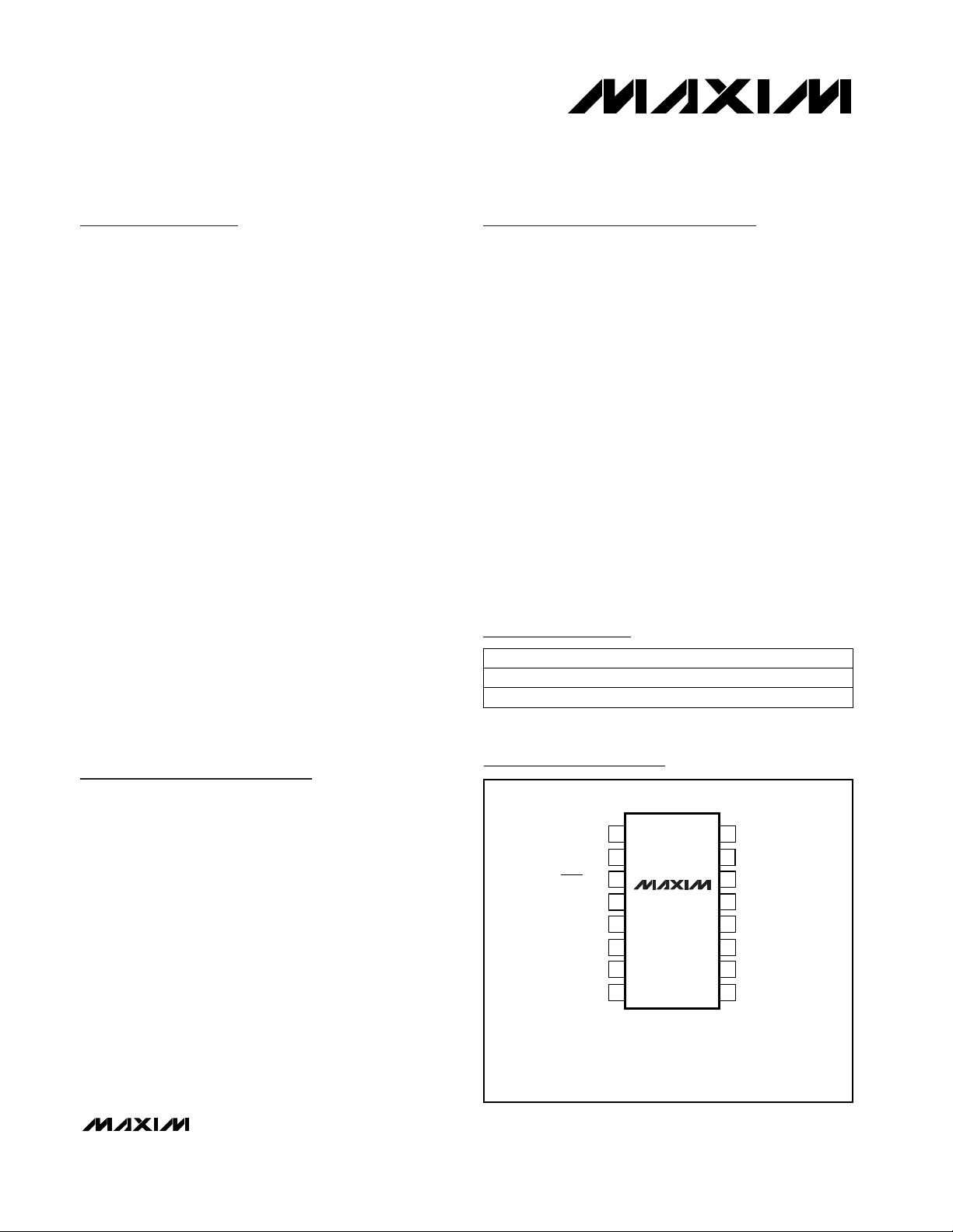
Pin Configuration
Ordering Information
Functional Diagrams appear at end of data sheet.
For price, delivery, and to place orders, please contact Maxim Distribution at 1-888-629-4642,
or visit Maxim’s website at www.maxim-ic.com.
TOP VIEW
1
RFIN V
GND
2
SHDN (D1)
CTRL (D0)
GND
GND
GND
RFOUT
3
MAX2232
4
MAX2233
5
6
7
8
16
GND
15
RAMP+ (N.C.)
14
RAMP- (N.C.)
13
V
12
V
11
TSET
10
N.C.
9
CC
CC
CC
GROUND OF OUTPUT STAGE CONNECTED TO PACKAGE SLUG.
( ) ARE FOR MAX2233.
PQSOP
Page 2
MAX2232/MAX2233
900MHz ISM-Band, 250mW Power Amplifiers
with Analog or Digital Gain Control
2 _______________________________________________________________________________________
ABSOLUTE MAXIMUM RATINGS
DC ELECTRICAL CHARACTERISTICS
(V
CC
= +2.7V to +5.5V, V
CTRL
= +2.2V, V
SHDN
= VD0= VD1= +2V, TA= -40°C to +85°C. No input signal applied, unless otherwise
noted. Typical values are at V
CC
= +3.6V and TA= +25°C.)
AC ELECTRICAL CHARACTERISTICS
(MAX2232/MAX2233 Evaluation Kit, VCC= +3.6V, V
CTRL
= +2.2V, SHDN = VCC(MAX2232), D0 = D1 = VCC(MAX2233),
P
RFIN
= 0dBm, ƒ
RFIN
= 915MHz, TA= +25°C, unless otherwise noted.)
Stresses beyond those listed under “Absolute Maximum Ratings” may cause permanent damage to the device. These are stress ratings only, and functional
operation of the device at these or any other conditions beyond those indicated in the operational sections of the specifications is not implied. Exposure to
absolute maximum rating conditions for extended periods may affect device reliability.
VCCto GND...........................................................-0.3V to +6.5V
SHDN, CTRL, D0, D1 to GND ....................-0.3V to (V
CC
+0.3V)
I
RFIN
....................................................................................10mA
RFIN Power (50Ω AC-coupled source). .........................+10dBm
Output Load VSWR. ................................................................6:1
Continuous Power Dissipation (T
A
= +70°C)
16-Pin PQSOP (derate 80mW/°C above +70°C) ................3W
Operating Temperature Range ...........................-40°C to +85°C
Storage Temperature Range .............................-65°C to +150°C
Lead Temperature (soldering, 10s) .................................+300°C
V
CTRL
≤ 0.4V (MAX2232)
V
SHDN
= 0.6V,
VD0= VD1= 0.6V
V
CTRL
= GND
V
SHDN
= GND (MAX2232),
VD0= VD1= GND (MAX2233)
V
SHDN
= 2.0V (MAX2232),
V
D0
= VD1= 2.0V (MAX2233)
MAX2232
SHDN (MAX2232), D0, D1 (MAX2233)
SHDN (MAX2232), D0, D1 (MAX2233)
MAX2232
V
CTRL
= 2.2V
CONDITIONS
1.5
mA20.3 25I
CC
Standby Supply Current
0.2 10
I
CC
V2.7 5.5V
CC
Supply Voltage Range
Shutdown Supply Current
µA
-1.5 1
CTRL Input Current
-1 1I
IL
µA
-1 10I
IH
Logic Input Current
V0.6V
CTRL
CTRL Input for Gain-Control
Mode
V2.0V
IH
Logic Input High
V0.6V
IL
Logic Input Low
V0.4V
CTRL
CTRL Input for Standby Mode
UNITSMIN TYP MAXSYMBOLPARAMETER
µA
120
VCC≤ 3.6V
VCC= 5.5V
VCC= 4.8V
(Notes 1, 2)
D0 = GND, D1 = VCC(MAX2233 only)
VCC= 3.6V (Note 1)
VCC= 3.0V
VCC= 2.7V
TA= T
MIN
to T
MAX
(Note 1)
CONDITIONS
25.4
dB23.9G
P
MHz902 928ƒ
IN
Frequency Range
Power Gain
dBm15.8P
OUT
Output Power, Medium-Power
Mode
22.9 23.9 24.9
dBm
22.5
21.6
P
OUT
Output Power
dB1.9 3.2∆P
OUT
Output Power Variation Over
Temperature
UNITSMIN TYP MAXSYMBOLPARAMETER
Page 3
MAX2232/MAX2233
900MHz ISM-Band, 250mW Power Amplifiers
with Analog or Digital Gain Control
_______________________________________________________________________________________ 3
AC ELECTRICAL CHARACTERISTICS (continued)
(MAX2232/MAX2233 Evaluation Kit, VCC= +3.6V, V
CTRL
= +2.2V, SHDN = VCC(MAX2232), D0 = D1 = VCC(MAX2233),
P
RFIN
= 0dBm, ƒ
RFIN
= 915MHz, TA= +25°C, unless otherwise noted.)
Note 1: Guaranteed by design.
Note 2: Operation outside this range is possible, but not characterized.
Note 3: Gain is monotonic with V
CTRL
.
Note 4: Input VSWR relative to input impedance in operating mode.
Note 5: Harmonics measured on evaluation kit, which provides some harmonic attenuation in addition to the rejection provided by
the IC. The combined suppression is specified.
Note 6: Time measured from SHDN (MAX2232) low-to-high transition to when output power is within 1dB of final value. Includes
effects of 1% tolerance capacitor.
Note 7: Time measured from SHDN (MAX2232) high-to-low transition to when output power is -20dB of final value. Includes effects
of 1% tolerance capacitors.
Note 8: Time from die temperature dropping below Thermal Shutdown Temperature, T
TH
, to when the device turns itself back on.
C
RAMP
= 0.22µF (Notes 1, 6) (MAX2232 only)
(Note 5)
Any load phase angle, P
RFIN
= +5dBm,
TA= T
MIN
to T
MAX
VCC= +2.7V to +5.5V,
6:1 VSWR at any phase angle,
P
RFIN
= +5dBm
CTRL = GND (MAX2232 only)
SHDN = D0 = D1 = GND
MAX2232 only
0.6V < V
CTRL
< 2.2V (MAX2232 only)
Z
SOURCE
= 50Ω (Note 1)
D0 = VCC, D1 = GND (MAX2233 only)
D0 = VCC, D1 = GND (MAX2233 only)
D0 = GND, D1 = VCC(MAX2233 only)
CTRL adjusted to give P
RFOUT
= +21dBm
(MAX2232 only)
CONDITIONS
ms0.9Autoramping Rise Time
dBc29Harmonic Suppression
6:1
Maximum Output Load VSWR
Without Damage (Note1)
dBc-60
Maximum Nonharmonic
Spurious Output Due to Load
Mismatch
dB
38
52
Off-Isolation
1.2:1∆VSWR
Input VSWR Change, Standby
Mode (Notes 1, 4)
1.4:1∆VSWR
Input VSWR Change, Shutdown
Mode (Notes 1, 4)
1.5:1VSWRInput VSWR
mA44.0I
CC
Supply Current, Low-Power
Mode
mA78.5I
CC
Supply Current, Medium-Power
Mode
%29PAE
Power-Added Efficiency at
+21dBm Output Power
%44PAEPower-Added Efficiency
dB23.6∆G
P
Gain-Control Range (Note 3)
dBm6.5P
OUT
Output Power, Low-Power Mode
UNITSMIN TYP MAXSYMBOLPARAMETER
P
RFIN
= 0dBm, VCC= +3.6V
RAMP+ = RAMP- = unconnected (Note 6)
C
RAMP
= 0.22µF (Notes 1, 7) (MAX2232 only)
C
TSET
= 0.22µF (Note 8)
°C145T
TH
Thermal Shutdown Temperature
µs0.4
ms3.2Autoramping Fall Time
Output Power Rise Time
ms900t
TH
Thermal Shutdown Timeout
Period
Page 4

LINEAR
SCALE
0
3V
1ms/div
MAX2232
OUTPUT POWER vs. SHUTDOWN CONTROL
MAX2232/33 toc10
C
RAMP
= 0.22µF
OUTPUT
POWER
SHUTDOWN
MAX2232/MAX2233
900MHz ISM-Band, 250mW Power Amplifiers
with Analog or Digital Gain Control
4 _______________________________________________________________________________________
Typical Operating Characteristics
(MAX2232/MAX2233 Evaluation Kit, VCC= +3.6V, CTRL = VCC, SHDN = D0 = D1 = VCC, P
RFIN
= 0dBm, f
RFIN
= 915MHz, TA= +25°C,
unless otherwise noted.)
0.001
0.01
1
0.1
10
100
2.5 3.53.0 4.0 4.5 5.0 5.5
SHUTDOWN SUPPLY CURRENT
vs. SUPPLY VOLTAGE
MAX2232/33 toc01
SUPPLY VOLTAGE (V)
SHUTDOWN SUPPLY CURRENT (µA)
TA = -40°C
TA = +25°C
TA = +85°C
0
10
5
20
15
25
30
2.5 3.5 4.03.0 4.5 5.0 5.5
MAX2232
STANDBY SUPPLY CURRENT
vs. SUPPLY VOLTAGE
MAX2232/33 toc02
SUPPLY VOLTAGE (V)
SUPPLY CURRENT (mA)
TA = -40°C
TA = +25°C
TA = +85°C
V
SHDN
= V
CC
V
CTRL
= GND
RFIN = UNCONNECTED
22
23
24
25
26
27
28
20
21
2.5 3.53.0 4.0 4.5 5.0 5.5
OUTPUT POWER vs. SUPPLY VOLTAGE
MAX2232/33 toc03
SUPPLY VOLTAGE (V)
OUTPUT POWER (dBm)
TA = +85°C
TA = -40°C
TA = +25°C
0
5
10
15
20
25
30
0.6 1.00.8 1.2 1.4 1.6 .1.8 2.0 2.2 2.4
MAX2232
OUTPUT POWER vs. GAIN CONTROL VOLTAGE
MAX2232/33 toc06
V
CTRL
(V)
OUTPUT POWER (dBm)
TA = -40°C
TA = +25°C
TA = +85°C
10
0
20
40
30
50
60
2.5 3.53.0 4.0 4.5 5.0 5.5
POWER-ADDED EFFICIENCY
vs. SUPPLY VOLTAGE
MAX2232/33 toc04
SUPPLY VOLTAGE (V)
POWER-ADDED EFFICIENCY (%)
TA = -40°C
TA = +25°C
TA = +85°C
5
10
15
20
25
30
902 915 928
OUTPUT POWER vs. FREQUENCY
MAX2232/33 toc05
FREQUENCY (MHz)
OUTPUT POWER (dBm)
MAX2233 (D0 = 0, D1 = 1)
MAX2233 (D0 = D1 = 1), AND MAX2232
MAX2233 (D0 = 1, D1 = 0)
3
8
18
13
23
28
10
25
55
40
70
85
-20 -10-15 -5 0 5 10 15
OUTPUT POWER AND POWER-ADDED EFFICIENCY
vs. INPUT POWER
MAX2232/33 toc07
INPUT POWER (dBm)
OUTPUT POWER (dBm)
PAE (%)
TA = -40°C
TA = -40°C
TA = +25°C
P
OUT
PAE
TA = +25°C
TA = +85°C
TA = +85°C
1.0
1.2
1.4
1.6
1.8
2.0
902 915 928
MAX2232
RFIN PORT VSWR vs. FREQUENCY
MAX2232/33 toc08
FREQUENCY (MHz)
VSWR
SHUTDOWN MODE
NORMAL OPERATION
STANDBY MODE
Page 5

MAX2232/MAX2233
900MHz ISM-Band, 250mW Power Amplifiers
with Analog or Digital Gain Control
_______________________________________________________________________________________ 5
Pin Description
PIN
FUNCTION
MAX2232 MAX2233
13 —
Negative Terminal of Output Power Ramp Capacitor. Connect capacitor, C
RAMP
, between
RAMP+ and RAMP- to control the rise and fall time of the output power ramp.
12 12 Input Stage Supply Voltage. Bypass with appropriate capacitors to GND.
11 11 Second Stage Supply Voltage. Bypass with appropriate capacitors to GND.
10 10
Thermal Shutdown Timeout Capacitor Terminal. Connect a capacitor from TSET to ground
to limit thermal cycling.
9 9, 13, 14 No Connection. Do not make a connection to this pin.
14 —
Positive Terminal of Output Power Ramp Capacitor. Connect capacitor, C
RAMP
, between
RAMP+ and RAMP- to control the rise and fall time of the output power ramp.
15 15
Bias Circuitry Ground. Connect directly to low-inductance ground plane. If vias are used,
separate them from other GND pin vias.
16 16 Bias Circuitry Supply Voltage. Bypass with appropriate capacitors to GND.
SLUG SLUG
Output Stage Ground. Provides additional thermal conduction, as well as a low-inductance
path to ground. Connect directly to low-inductance ground plane.
NAME
RAMP-
V
CC
V
CC
TSET
N.C.
RAMP+
GND
V
CC
GND
8 8 Open-Collector, RF Output Port. Connect output matching network to this pin.RFOUT
5, 6 5, 6
Second Stage Ground. Connect directly to low-inductance ground plane. If vias are used,
separate them from other GND pin vias.
GND
7 7
Output Stage Ground. Connect directly to low-inductance ground plane. If vias are used,
separate them from other GND pin vias.
GND
4 —
Analog Gain-Control Input. Apply a voltage between 0.6V and 2.2V to vary the gain of the
PA. Drive CTRL below 0.4V to place the device in standby mode. Drive CTRL above 2.2V to
place the device in peak output power mode.
CTRL
3 —
Shutdown Control Input. Drive SHDN low to place the device in shutdown mode. Drive high
for normal operation.
SHDN
— 3
Digital Gain/Shutdown Control Input. MSB of the 2-bit digital output power control. D0 and
D1 set the output power to one of three discrete levels. To place the device in shutdown,
drive D0 and D1 low (Table 2).
D1
— 4
Digital Gain/Shutdown Control Input. LSB of the 2-bit digital output power control. D0 and
D1 set the output power to one of three discrete levels. To place the device in shutdown,
drive D0 and D1 low (Table 2).
D0
1 1 RF Input Port. Requires external matching network and blocking capacitor.RFIN
2 2
Input Stage Ground. Connect directly to low-inductance ground plane. If vias are used,
separate them from other GND pin vias.
GND
Page 6

MAX2232/MAX2233
900MHz ISM-Band, 250mW Power Amplifiers
with Analog or Digital Gain Control
6 _______________________________________________________________________________________
Detailed Description
The MAX2232/MAX2233 are nonlinear power amplifiers
(PAs) intended for constant envelope applications (FM,
FSK, GMSK). The devices operate over the 902MHz to
928MHz frequency range and provide typically 250mW
of output power and 44% efficiency from a single +2.7V
to +5.5V supply. Both devices typically provide 24dB of
gain, which is adjustable over a continuous 24dB range
through an analog voltage on CTRL of the MAX2232 or
in two 10dB steps through the 2-bit programmable gain
inputs (D0, D1) on the MAX2233. A low-power shutdown
mode on both devices reduces supply current to 0.2µA.
All bias, gain control, and temperature-sensing circuitry
is provided on-chip to save board space and reduce
component count. The signal path includes a variable
gain amplifier (VGA), an output driver, and an output
power transistor. On-chip interstage matching networks
are provided for optimal loading and power transfer.
Internal bias circuitry responds to CTRL and SHDN of
the MAX2232, or to the 2-bit gain/shutdown control
DAC of the MAX2233, providing optimum biasing and
efficiency as well as shutdown and ramp control functions. A unique temperature-sensing circuit protects the
device from overheating by shutting down the PA until
a safe temperature is resumed.
The devices come in a 16-pin PQSOP package, which
incorporates a slug on the bottom of the device to
increase heat conduction and provide a low inductance path to ground.
RF Input Stage (Variable Gain Amplifier)
The input stage includes a variable gain amplifier
(VGA) with 24dB gain-control range. With the appropriate matching network, the input VSWR is nominally
1.5:1 during operation and the change in VSWR is only
1.2:1, relative to normal operation. This stage remains
active during standby mode (MAX2232) to provide a
constant input impedance but is off during shutdown
mode (MAX2232/MAX2233). AC-couple this port with a
DC-blocking capacitor.
RF Second Stage (Driver)
The driver provides gain to overcome interstage matching losses and to produce a signal large enough to
drive the output power transistor into saturation. The
driver stage is off during standby (MAX2232) and shutdown (MAX2232/MAX2233) modes.
RF Output Stage
(Output Power Transistor)
The output power transistor delivers +24dBm of output
power from a single +3.6V supply. The transistor’s
open-collector output requires a pull-up inductor to
V
CC
for proper biasing, as well as a proper output
matching network to ensure optimum output power.
Connect the output matching network to RFOUT (pin
8). See the Typical Application Circuit for bias and
matching components suitable for 900MHz operation.
The ground of the output stage is connected to a metal
slug on the bottom of the MAX2232/MAX2233’s 16-pin
PQSOP package. The metal slug increases heat conduction and provides a low-inductance path to ground.
Solder the metal slug to the PC-board ground plane.
___________________________MAX2232
Analog Gain Control
and Power Management
Shutdown Mode
Drive the shutdown (SHDN) pin below 0.6V to place the
MAX2232 in shutdown mode. The VGA, driver, and output transistor are off in shutdown mode and the supply
current is typically reduced to 0.2µA. When SHDN is
above 2.0V, the device is enabled.
Standby Mode
Drive SHDN above 2.0V and CTRL below 0.4V to place
the MAX2232 in standby mode. In standby mode, the
VGA remains biased while the driver and output transistor are disabled. Supply current is typically 20mA in
standby mode. This mode allows the device to maintain
a good input VSWR while maintaining 38dB of isolation.
This is useful to users who drive the PA with a direct
modulated VCO, where pulling of the VCO results from
changes in the input VSWR.
Analog Gain Control
The voltage applied to the gain-control (CTRL) pin varies
the output power of the MAX2232 continuously over a
24dB range. An internal comparator holds the PA to a
constant peak output power if V
CTRL
is above 2.2V. For
V
CTRL
below 0.4V, the PA is in standby mode. CTRL pre-
sents a high input impedance, allowing the V
CTRL
voltage
to be set with a resistor-divider or a voltage output DAC.
Output Power Autoramping
The internal bias circuitry of the MAX2232 automatically
ramps the output power of the PA down or up at a constant rate (in W/sec) when switched in or out of shutdown mode. The output power is ramped to the level set
by V
CTRL
on the MAX2232. The output power rise and
fall time ramp is set by placing a capacitor, C
RAMP
,
between RAMP+ and RAMP-. This provides an easy
means of avoiding spectral splatter and complying with
transmit mask requirements, without using a separate
controller. The output power rise and fall time is set by
the value of C
RAMP
.
Page 7

___________________________MAX2233
Digital Gain Control
and Power Management
The MAX2233 responds to logic-level signals at the
device’s 2-bit DAC inputs, D0 and D1, placing the
device in shutdown mode or into one of three discrete
output power levels. See Table 2 for operating modes
and output power levels. Setting D0 and D1 to a logiclevel low places the device in shutdown mode and
reduces supply current to 0.2µA. The VGA, driver, and
output stage are off in shutdown mode, while the input
impedance is only slightly changed. Setting D0 and D1
to one of the other three modes adjusts the output
power to one of three discrete levels in 10dB steps.
Thermal Shutdown
The MAX2232/MAX2233 feature a thermal shutdown
mode that helps to protect the device from damage
when the die temperature becomes excessive. If the
temperature of the die exceeds the thermal shutdown
temperature, TTH, the VGA is forced into a low-gain
mode and output power is reduced to a minimum. After
the PA’s die temperature drops below T
TH
, the device
remains in thermal shutdown mode for the thermal shutdown timeout period, tTH. A single capacitor, C
TSET
,
from TSET to ground sets tTH. The thermal shutdown
timeout period helps to limit device thermal cycling that
results if the source of the excessive temperature is not
removed. tTHis set by the value of C
TSET
.
Applications Information
Proper attention to voltage supply bypassing is essential for high-frequency RF circuit stability. Bypass V
CC
with 0.1µF, 10nF, and 100pF capacitors in parallel with
each other to ground. Use separate vias to the ground
plane for each of the bypass capacitors and minimize
trace length to reduce inductance. Use separate vias to
the ground plane for each ground pin. Use low-inductance ground connections.
Decouple SHDN, CTRL, D0, and D1 with 0.1µF capacitors to ground to minimize noise on the internal bias cell.
Use a series resistor (typically 100Ω) to further reduce
coupling of high-frequency signals into the control pins.
MAX2232/MAX2233
900MHz ISM-Band, 250mW Power Amplifiers
with Analog or Digital Gain Control
_______________________________________________________________________________________ 7
MODE
Standby > 2.0V
< 0.6V
V
SHDN
V
CTRL
X
≤ 0.4V
OUTPUT POWER
(P
RFIN
= 0dBm,
V
CC
= +3.6V)
< -35dBm
< -35dBm
Variable Gain > 2.0V
0.6V ≤ V
CTRL
< 2.2V
0dBm to +24dBm
Maximum Gain > 2.0V > 2.2V +24 dBm
Shutdown
Table 1. MAX2232 Operating Modes
X = Don’t care
Table 2. MAX2233 Operating Modes
Truth Table
MODE
Shutdown
Low Power 0
0
D1 D0
0
1
OUTPUT POWER
(P
RFIN
= 0dBm,
VCC= +3.6V)
< -35dBm
+6.5dBm
Medium Power 1 0 +15dBm
High Power 1 1 +24dBm
Functional Diagrams
MAX2232
VGA DRIVER
TEMP
SENSOR
RFOUT
TSET
2
16 15
5, 6 7, SLUG
8
10
SHDN
RAMP+
14
3
11
12
1
13
RAMP-
V
CC
V
CC
4
CTRL
RFIN
BIAS
GND
V
CC
GND
GND GND
TSET
MAX2233
VGA DRIVER
TEMP
SENSOR
RFOUT
2
16 15
5, 6 7, SLUG
10
D0
4
3
11
12
1
D1
V
CC
V
CC
RFIN
BIAS
GND
V
CC
GND
GND GND
8
2-BIT
DAC
Page 8

MAX2232/MAX2233
900MHz ISM-Band, 250mW Power Amplifiers
with Analog or Digital Gain Control
Maxim cannot assume responsibility for use of any circuitry other than circuitry entirely embodied in a Maxim product. No circuit patent licenses are
implied. Maxim reserves the right to change the circuitry and specifications without notice at any time.
8 _____________________Maxim Integrated Products, 120 San Gabriel Drive, Sunnyvale, CA 94086 408-737-7600
© 2000 Maxim Integrated Products Printed USA is a registered trademark of Maxim Integrated Products.
Typical Application Circuit
Package Information
0.22µF
RFIN
15nH
100pF
100pF
68pF
1
RFIN
MAX2232
2
MAX2233
GND GND
3
SHDN
(D1)
4
CTRL
(D0)
5
GND
6
GND
RAMP+
(N.C.)
RAMP-
(N.C.)
V
16
V
CC
15
14
13
12
V
CC
11
V
CC
C
RAMP
0.22µF
100pF
10nF 0.1µF
10nF 0.1µF100pF
10nF 0.1µF100pF
CC
V
CC
V
CC
RFOUT
NOTES: ( ) APPLIES TO MAX2233.
BACKSIDE SLUG MUST BE SOLDERED
0.22µF
3.6pF
TO GROUNDPLANE.
2.55nH
7
GND
8
RFOUT
27nH
100pF 10nF 0.1µF
TSET
N.C.
10
9
C
TSET
0.22µF
V
CC
PSSOPPS.EPS
 Loading...