

For free samples & the latest literature: http://www.maxim-ic.com, or phone 1-800-998-8800.
For small orders, phone 1-800-835-8769.
General Description
The MAX221E is a +5V powered, single transmit/
receive RS-232 and V.28 communications interface with
automatic shutdown/wake-up features and high data
rate capabilities.
The MAX221E features enhanced electrostatic discharge
(ESD) protection. Both the transmitter output and receiver
input are protected to ±15kV using the IEC 1000-4-2 AirGap Discharge Method, to ±8kV using the IEC 1000-4-2
Contact Discharge Method, and to ±15kV using the
Human Body Model.
The MAX221E achieves a low 1µA supply current with
Maxim’s revolutionary AutoShutdown™ feature.
AutoShutdown saves power without changes to the
existing BIOS or operating system by entering lowpower shutdown mode when the RS-232 cable is disconnected or when the transmitter of the connected
peripheral is off. The MAX221E wakes up and drives the
INVALID pin high when an active RS-232 cable is connected, signaling the host that a peripheral is connected
to the communications port.
The MAX221E is available in a 16-pin SSOP package as
well as a 16-pin TSSOP that uses 50% less board space
than a 16-pin SO.
Applications
Maintenance/Diagnostic Ports
Industrial Systems
Telecommunications
Set-Top Boxes
Features
♦ Single RS-232 Transceiver in a Small 16-Pin TSSOP
♦ ESD Protection for RS-232 I/O Pins
±15kV—Human Body Model
±8kV—IEC 1000-4-2, Contact Discharge
±15kV—IEC 1000-4-2, Air-Gap Discharge
♦ Latchup Free
♦ 1µA Supply Current
♦ AutoShutdown Saves Power without Changes
to BIOS
♦ Guaranteed 250kbps Data Rate
MAX221E
±15kV ESD-Protected, +5V, 1µA, Single RS-232
Transceiver with AutoShutdown
________________________________________________________________
Maxim Integrated Products
1
Typical Operating Circuit
19-1527; Rev 0; 8/99
PART
MAX221ECUE
MAX221ECAE
MAX221EEUE 40°C to +85°C
0°C to +70°C
0°C to +70°C
TEMP. RANGE PIN-PACKAGE
16 TSSOP
16 SSOP
16 TSSOP
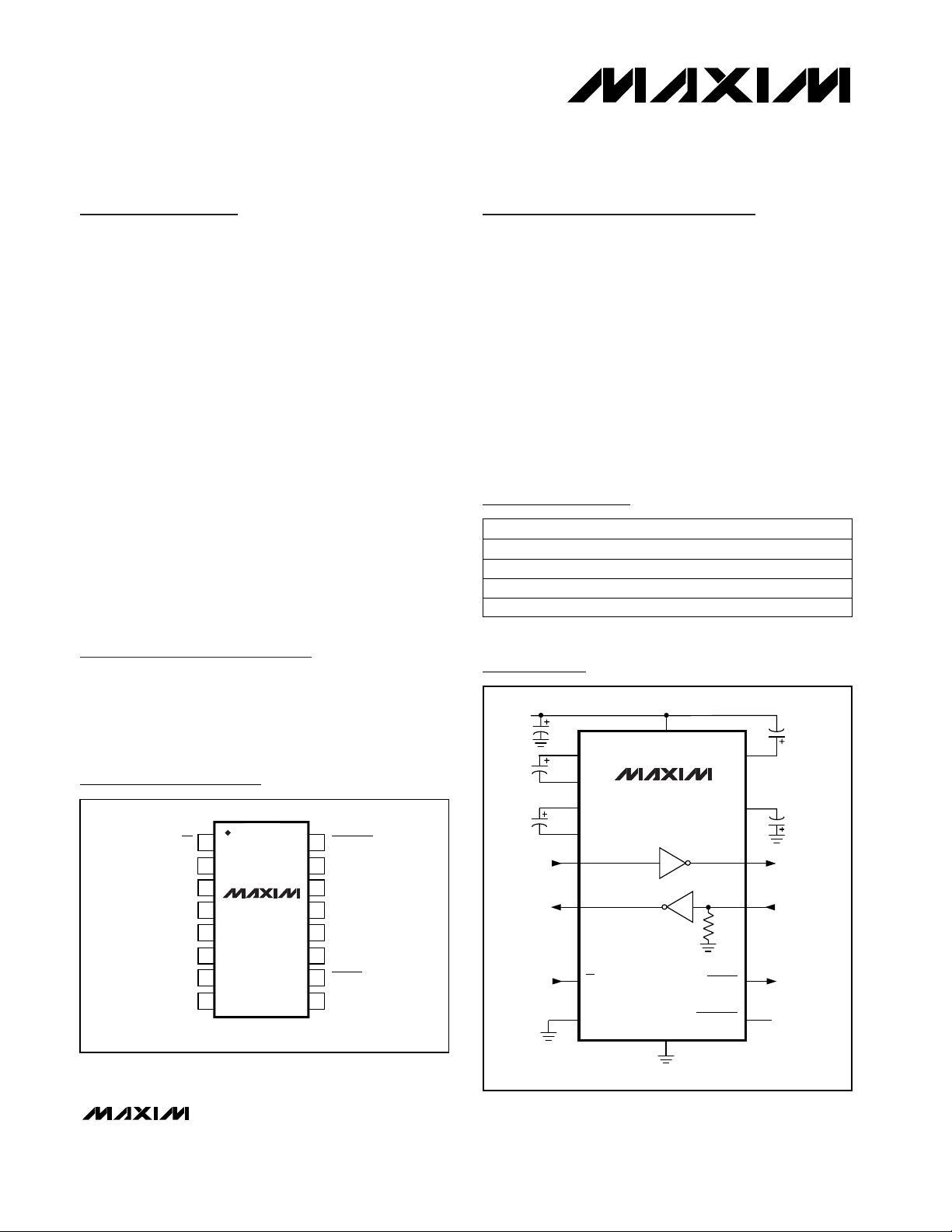
Pin Configuration
Ordering Information
AutoShutdown is a trademark of Maxim Integrated Products.
MAX221EEAE 40°C to +85°C 16 SSOP
TOP VIEW
1
EN FORCEOFF
C1+
2
V+
3
4
C1-
C2+
5
C2-
6
V-
7
RIN
8
16
15
V
CC
14
GND
MAX221E
TSSOP/SSOP
13
12
11
10
9
TOUT
FORCEON
TIN
INVALID
ROUT
C
BYPASS
0.1µF
0.1µF
0.1µF
C1
C2
+5V
11
12
2
4
5
6
1
C1+
C1-
C2+
C2-
TIN
ROUT9
EN
FORCEON
15
V
CC
MAX221E
GND
14
V+
V-
TOUT 13
RIN 8
5k
INVALID
FORCEOFF
CAPACITORS MAY BE
POLARIZED OR UNPOLARIZED.
3
7
10
16
C3
0.1µF
C4
0.1µF
TO POWERMANAGEMENT
UNIT
V
CC
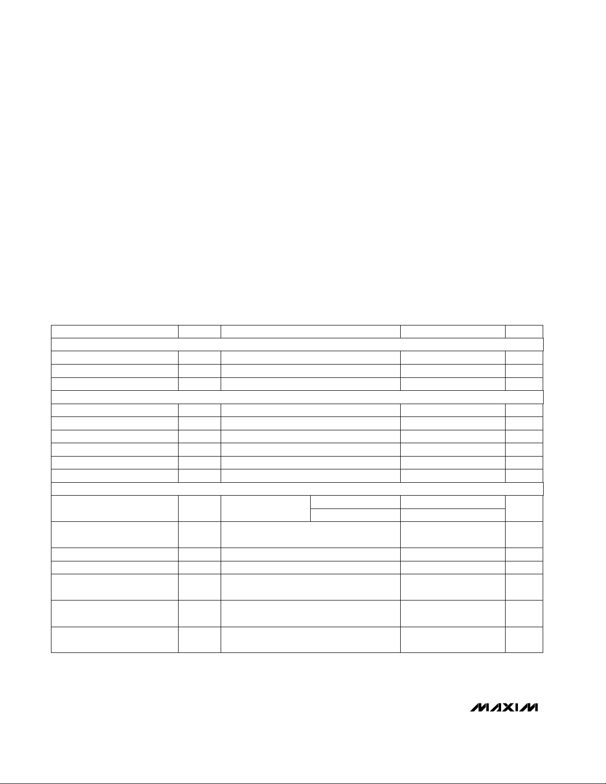
MAX221E
±15kV ESD-Protected, +5V, 1µA, Single RS-232
Transceiver with AutoShutdown
2 _______________________________________________________________________________________
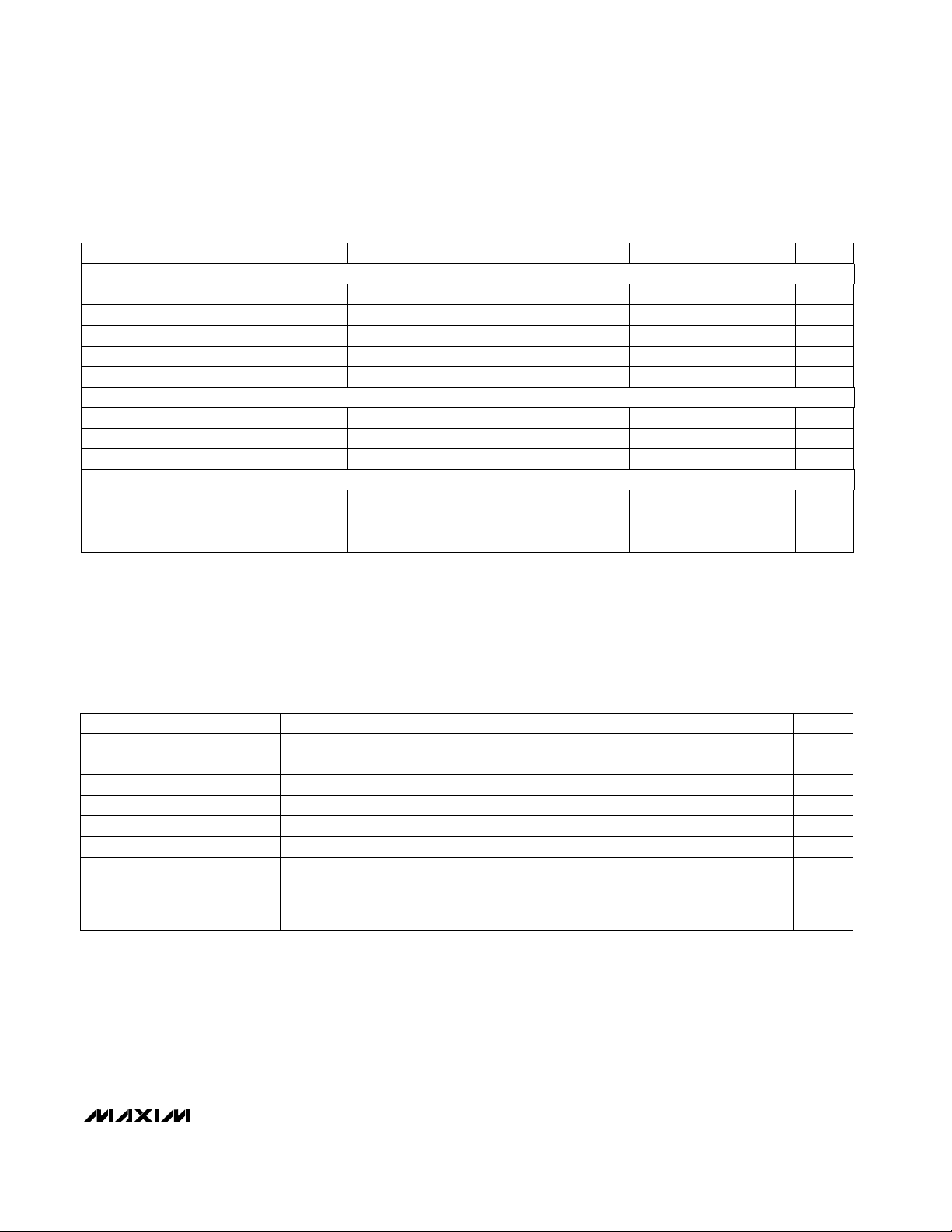
ABSOLUTE MAXIMUM RATINGS
ELECTRICAL CHARACTERISTICS
(V
CC
= +5V ±10%, C1–C4 = 0.1µF, TA= T
MIN
to T
MAX
, unless otherwise noted. Typical values are at TA= +25°C.)
Stresses beyond those listed under “Absolute Maximum Ratings” may cause permanent damage to the device. These are stress ratings only, and functional
operation of the device at these or any other conditions beyond those indicated in the operational sections of the specifications is not implied. Exposure to
absolute maximum rating conditions for extended periods may affect device reliability.
VCC..........................................................................-0.3V to +6V
V+ ...............................................................(V
CC
- 0.3V) to +14V
V- ...........................................................................-14V to +0.3V
Input Voltages
TIN............................................................-0.3V to (V+ + 0.3V)
RIN...................................................................................±30V
FORCEON, FORCEOFF, EN ..................-0.3V to (V
CC
+ 0.3V)
Output Voltages
TOUT ................................................(V- - 0.3V) to (V+ + 0.3V)
ROUT, INVALID ......................................-0.3V to (V
CC
+ 0.3V)
Short-Circuit Duration, TOUT .....................................Continuous
Continuous Power Dissipation (T
A
= +70°C)
16-Pin TSSOP (derated 6.7mW/°C above +70°C) .......533mW
16-Pin SSOP (derated 7.1mW/°C above +70°C) .........571mW
Operating Temperature Range
MAX221EC_ _. ....................................................0°C to +70°C
MAX221EE_ _ ..................................................-40°C to +85°C
Maximum Junction Temperature .................................... +150°C
Storage Temperature Range ........................... -65°C to +150°C
Lead Temperature (soldering, 10sec) ............................ +300°C
Figure 3
Figure 3
No load, TA= +25°C
Figure 3
I
SOURCE
= 1.0mA
I
SINK
= 1.6mA
CONDITIONS
ICC= 1µA, Figure 3
ROUT; I
SINK
= 3.2mA
Figure 3
TIN, EN, FORCEOFF, FORCEON
TA= +25°C, Figure 1
EN = VCC, 0 ≤ ROUT ≤ V
CC
TIN = 0 to V
CC
ROUT; I
SOURCE
= 1.0mA
µs30t
INVL
Receiver Positive or Negative
Threshold to INVALID Low
µs1t
INVH
Receiver Positive or Negative
Threshold to INVALID High
µs250t
WU
Receiver Threshold to
Transmitter Enabled
VVCC- 0.6
INVALID Output Voltage High
V0.4
INVALID Output Voltage Low
V
-0.3 0.3
Receiver Input Threshold,
Transmitter Disabled
-2.7
Positive threshold
V
2.7
Receiver Input Threshold,
Transmitter Enabled
µA
±0.05 ±10
Negative threshold
Output Leakage Current
V
3.5
V
OH
Output Voltage High
mA
510
I
CC
VCCSupply Current
UNITSMIN TYP MAXSYMBOLPARAMETER
V
0.4
V
OL
Output Voltage Low
V
0.8
V
IL
Input Threshold Low
µA
110
I
SHDN
Shutdown Supply Current
µA
110
I
AS
AutoShutdown Supply Current
µA
±1
Input Leakage Current
EN, FORCEOFF, TIN
V
2.4
V
IH
Input Threshold High
DC CHARACTERISTICS
LOGIC INPUTS
AUTOSHUTDOWN
MAX221E
±15kV ESD-Protected, +5V, 1µA, Single RS-232
Transceiver with AutoShutdown
_______________________________________________________________________________________ 3
TIMING CHARACTERISTICS
(VCC= +5V ±10%, C1–C4 = 0.1µF, TA = T
MIN
to T
MAX
, unless otherwise noted. Typical values are at TA= +25°C.)
ELECTRICAL CHARACTERISTICS (continued)
(V
CC
= +5V ±10%, C1–C4 = 0.1µF, TA= T
MIN
to T
MAX
, unless otherwise noted. Typical values are at TA= +25°C.)
Note 1: Transmitter skew is measured at the transmitter zero crosspoints.
RL= 3kΩ to 7kΩ, CL= 50pF to 1000pF,
VCC= 4.5V
CONDITIONS
kbps
250
Maximum Data Rate
UNITSMIN TYP MAXSYMBOLPARAMETER
TA= +25°C, VCC= 5V, RL= 3kΩ to 7kΩ,
CL= 500pF to 1000pF, measured from
-3V to +3V or +3V to -3V
(Note 1)
Normal operation
Normal operation
CL= 150pF
V/µs3630Transition-Region Slew Rate
ns
50
|t
PHL tPLH
|Receiver Skew
ns
200
|t
PHL tPLH
|Transmitter Skew
ns
200
Receiver Output Disable Time
ns
300
Receiver Output Enable Time
ms
0.15
t
PHL,tPLH
Receiver Propagation Delay
CONDITIONS UNITSMIN TYP MAXSYMBOLPARAMETER
V
CC
= V+ = V- = 0, V
OUT
= ±2V
Driver loaded with 3kΩ to ground
TA= +25°C, V
CC
= 5V
VCC= 5V, no hysteresis in shutdown
TA= +25°C, VCC= 5V
TA= +25°C, VCC= 5V
mA±10 ±60Output Short-Circuit Current
Ω300Output Resistance
V±5 ±9Output Voltage Swing
kΩ357Input Resistance
V0.5Input Hysteresis
V1.7 2.4Input Threshold High
V0.8 1.2Input Threshold Low
V-25 25Input Voltage Range
IEC 1000-4-2 Air-Gap Discharge
kV
±15
RIN, TOUT IEC 1000-4-2 Contact Discharge ±8
Human Body Model ±15
RECEIVER INPUT
TRANSMITTER OUTPUT
ESD PROTECTION
MAX221E
±15kV ESD-Protected, +5V, 1µA, Single RS-232
Transceiver with AutoShutdown
4 _______________________________________________________________________________________
NAME FUNCTION
1
EN
Receiver Enable Control. Drive low for normal operation. Drive high to force the receiver output
(ROUT) into a high-impedance state.
2 C1+ Positive Terminal of the Voltage Doubler Charge-Pump Capacitor
PIN
3 V+ Positive Voltage Generated by the Charge Pump
4 C1- Negative Terminal of the Voltage Doubler Charge-Pump Capacitor
8 RIN RS-232 Receiver Input, ±15kV ESD protected
7 V- Negative Voltage Generated by the Charge Pump
6 C2- Negative Terminal of the Inverting Charge-Pump Capacitor
5 C2+ Positive Terminal of the Inverting Charge-Pump Capacitor
13 TOUT RS-232 Transmitter Output, ±15kV ESD Protected
12 FORCEON
Drive high to override automatic circuitry, keeping transmitter and charge pump on. FORCEOFF
must be high (Table 1).
11 TIN TTL/CMOS Transmitter Input
10
INVALID
Output of the Invalid Signal Detector. INVALID is pulled low if no valid RS-232 level is present on
the receiver input.
9 ROUT TTL/CMOS Receiver Output
Pin Description
14 GND Ground
15 V
CC
+4.5V to +5.5V Supply Voltage
16
FORCEOFF
Force-Off Input, active low. Drive low to shut down transmitter, receiver, and on-board charge
pump. This overrides all automatic circuitry and FORCEON (Table 1).
-10
-6
-8
-2
-4
2
0
4
8
6
10
0
1000
2000
3000
4000
5000
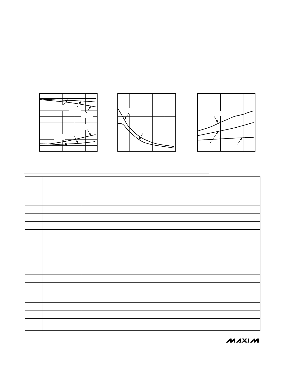
TRANSMITTER OUTPUT
VOLTAGE vs. LOAD CAPACITANCE
MAX221Etoc01
LOAD CAPACITANCE (pF)
TRANSMITTER OUTPUT VOLTAGE (V)
250kbps
250kbps
120kbps
20kbps
20kbps
120kbps
0
10
20
30
40
50
0
1000
2000
3000
4000
5000
OPERATING SUPPLY
CURRENT vs. LOAD CAPACITANCE
MAX221Etoc03
LOAD CAPACITANCE (pF)
SUPPLY CURRENT (mA)
250kbps
20kbps
120kbps
Typical Operating Characteristics
(VCC= +5V, 250kbps data rate, 0.1µF capacitors, transmitter loaded with 3kΩ and CL, TA= +25°C, unless otherwise noted.)
50
SLEW RATE vs.
LOAD CAPACITANCE
40
+SLEW
30
20
SLEW RATE (V/µs)
10
0
0
-SLEW
1000
2000
LOAD CAPACITANCE (pF)
3000
4000
MAX221Etoc02
5000

MAX221E
±15kV ESD-Protected, +5V, 1µA, Single RS-232
Transceiver with AutoShutdown
_______________________________________________________________________________________ 5
_______________Detailed Description
Dual Charge-Pump Voltage Converter
The MAX221E’s internal power supply consists of a
dual charge pump that provides a positive output voltage (doubling charge pump) and negative output voltage (inverting charge pump) from a single +5V supply.
The charge pumps operate in continuous mode. Each
charge pump requires a flying capacitor (C1, C2) and a
reservoir capacitor (C3, C4) to generate the V+ and Vsupplies.
RS-232 Transmitter
The transmitter is an inverting level translator that converts CMOS-logic levels to 5.0V EIA/TIA-232 levels. It
guarantees a 250kbps data rate with worst-case loads
of 3kΩ in parallel with 1000pF.
When FORCEOFF is driven to ground, or when the
AutoShutdown circuitry senses invalid voltage levels on
the receiver input, the transmitter is disabled and the
output is forced into a high-impedance state. The transmitter input does not have a pull-up resistor.
RS-232 Receiver
The MAX221E’s receiver converts RS-232 signals to
CMOS-logic output levels. The receiver has an inverting
three-state output and can be active or inactive. In
shutdown (FORCEOFF = low) or in AutoShutdown, the
receiver is active (Table 1). Drive EN high to place the
receiver in a high-impedance state. The receiver is
high-impedance when the MAX221E is in shutdown
(FORCEOFF = low).
The MAX221E’s INVALID output is pulled low when
there is no valid RS-232 signal level detected on the
receiver input. INVALID is functional in any mode
(Figures 2 and 3).
AutoShutdown
The MAX221E achieves 1µA supply current with
Maxim’s AutoShutdown feature, which operates when
FORCEON is low and FORCEOFF is high. When the
device senses no valid signal levels on the receiver
input for 30µs, the on-board charge pump and driver
are shut off, reducing supply current to 1µA. This
occurs if the RS-232 cable is disconnected or the connected peripheral transmitter is turned off. The
MAX221E turns on again when a valid level is applied
to the RS-232 receiver input. As a result, the system
saves power without changes to the existing BIOS or
operating system.
Table 1 and Figure 2c summarize the MAX221E operating modes. FORCEON and FORCEOFF override
AutoShutdown. When neither control is asserted, the
device selects between these states automatically,
based on the receiver input level. Figures 2a, 2b, and
3a depict valid and invalid RS-232 receiver levels.
Figure 3 shows the input levels and timing diagram for
AutoShutdown operation.
A device or another system with AutoShutdown connected to the MAX221E may need time to wake up.
Figure 4 shows a circuit that forces the transmitter on
for 100ms, allowing enough time for the other system to
realize that the MAX221E is awake. If the other system
transmits valid RS-232 signals within that time, the
RS-232 ports on both systems remain enabled.
When shut down, the device’s charge pumps turn off,
V+ is pulled to VCC, V- is pulled to ground, and the
transmitter output is high impedance. The time required
to exit shutdown is typically 100µs (Figure 3b).
Figure 1. Shutdown Current Test Circuit
I
+5V
C
BYPASS
0.1µF
C1
0.1µF
C2
0.1µF
SHDN
2
C1+
4
C1-
5
C2+
6
C2-
11
TIN
ROUT
9
15
V
CC
MAX221E
V+
V-
TOUT 13
RIN 8
5k
C3
0.1µF
3
7
C4
0.1µF
3k
1
12
EN
FORCEON
TO POWER-
10
MANAGEMENT
UNIT
16
GND
INVALID
FORCEOFF
14

MAX221E
±15kV ESD-Protected, +5V, 1µA, Single RS-232
Transceiver with AutoShutdown
6 _______________________________________________________________________________________
1 No
Shutdown
(AutoShutdown)
High-Z1 High-Z0
1
1
1
OPERATION
STATUS
X0
VALID
RECEIVER
EN
X
Shutdown
(Forced Off)
X
Normal Operation
(Forced On)
X0
Yes
Normal Operation
(AutoShutdown)
No
Yes0
0
High-Z
Active
Active
High-Z
TOUT
Active
High-Z
Active
0
FORCEOFF
1
0
1
1
1
1
High-Z
High-Z
Active
Active
ROUT
High-Z
Active
Active
X
FORCEON
1
X
1
0
0
0
RS-232 SIGNAL PRESENT
AT RECEIVER INPUT
INVALID OUTPUT
Yes High
No Low
Table 1. Output Control Truth Table
Table 2. INVALID Truth Table
Figure 2c. AutoShutdown Logic
Figure 2b. Transmitter Enabled Using AutoShutdown
Figure 2a. Entering 1µA Supply Mode via AutoShutdown
x = Don’t care
+0.3V
TO MAX221E
RIN
COUNTER
-0.3V
* TRANSMITTER IS DISABLED, REDUCING SUPPLY CURRENT TO 1µA IF
RECEIVER INPUT IS BETWEEN +0.3V AND -0.3V FOR AT LEAST 30µs.
30µs
R
POWER SUPPLY
AND TRANSMITTER
INVALID
+2.7V
RIN
COUNTER
-2.7V
* TRANSMITTER IS ENABLED IF:
RECEIVER INPUT IS GREATER THAN +2.7V OR LESS THAN -2.7V.
RECEIVER INPUT HAS BEEN BETWEEN +0.3V AND -0.3V FOR LESS THAN 30µs.
30µs
R
TO MAX221E
POWER SUPPLY
INVALID
FORCEOFF
FORCEON
INVALID
INVALID IS AN INTERNALLY GENERATED SIGNAL USED BY
AUTOSHUTDOWN LOGIC AND APPEARS AS AN OUTPUT.
POWER DOWN IS ONLY AN INTERNAL SIGNAL. IT CONTROLS THE
OPERATIONAL STATUS OF THE TRANSMITTER AND POWER SUPPLIES.
POWER DOWN

Software-Controlled Shutdown
For direct software control, use INVALID to indicate a
DTR or Ring Indicator signal. Connect FORCEOFF and
FORCEON together to disable AutoShutdown so the
line acts like a SHDN input.
±15kV ESD Protection
As with all Maxim devices, ESD-protection structures
are incorporated on all pins to protect against electrostatic discharges encountered during handling and
assembly. The driver output and receiver input of the
MAX221E have extra protection against static electricity. Maxim’s engineers have developed state-of-the-art
structures to protect these pins against ESD of ±15kV
without damage. The ESD structures withstand high
ESD in all states: normal operation, shutdown, and
powered down. After an ESD event, Maxim’s E versions
keep working without latchup, whereas competing
RS-232 products can latch and must be powered down
to remove latchup.
ESD protection can be tested in various ways; the transmitter output and receiver input of the MAX221E are
characterized for protection to the following limits:
1) ±15kV using the Human Body Model
2) ±8kV using the Contact-Discharge Method
specified in IEC 1000-4-2
3) ±15kV using IEC 1000-4-2’s Air-Gap Method
ESD Test Conditions
ESD performance depends on a variety of conditions.
Contact Maxim for a reliability report that documents
test setup, test methodology, and test results.
Human Body Model
Figure 5a shows the Human Body Model, and Figure
5b shows the current waveform it generates when discharged into a low impedance. This model consists of
a 100pF capacitor charged to the ESD voltage of interest, which is then discharged into the test device
through a 1.5kΩ resistor.
IEC 1000-4-2
The IEC 1000-4-2 standard covers ESD testing and
performance of finished equipment; it does not specifically refer to integrated circuits. The MAX221E helps
you design equipment that meets Level 4 (the highest
level) of IEC 1000-4-2, without the need for additional
ESD-protection components.
The major difference between tests done using the
Human Body Model and IEC 1000-4-2 (Figure 6) is
higher peak current in the IEC 1000-4-2 because series
resistance is lower in the IEC 1000-4-2 model. Hence,
MAX221E
±15kV ESD-Protected, +5V, 1µA, Single RS-232
Transceiver with AutoShutdown
_______________________________________________________________________________________ 7
Figure 3. AutoShutdown Trip Levels
a)
b)
Figure 4. AutoShutdown with Initial Turn-On to Wake Up a
Mouse or Another System
+2.7V
+0.3V
0
-0.3V
RECEIVER INPUT LEVEL
-2.7V
RECEIVER
INPUT
VOLTAGE
(V)
V
CC
INVALID
OUTPUT
(V)
0
V+
V
CC
0
V-
TRANSMITTER ENABLED, INVALID HIGH
INDETERMINATE
AUTOSHUTDOWN, TRANSMITTER DISABLED,
1µA SUPPLY CURRENT, INVALID LOW
INDETERMINATE
TRANSMITTER ENABLED, INVALID HIGH
t
INVL
t
INVH
INVALID
REGION
t
WU
POWER-
MANAGEMENT
UNIT
MASTER SHDN LINE
0.1µF 1MΩ
FORCEOFF
FORCEON
MAX221E

the ESD that withstands voltage measured to IEC 10004-2 is generally lower than that measured using the
Human Body Model. Figure 6a shows the IEEE 1000-42 model and Figure 6b shows the current waveform for
the ±8kV IEC 1000-4-2 Level 4 ESD Contact-Discharge
test.
The Air-Gap Method involves approaching the device
with a charged probe. The Contact-Discharge Method
connects the probe to the device before the probe is
energized.
Machine Model
The Machine Model for ESD tests all pins, using a
200pF storage capacitor and zero discharge resistance. Its objective is to emulate the stress caused not
only by RS-232 inputs and outputs, but also by contact
that occurs due to handling and assembling during
manufacturing. Therefore, after PC board assembly, the
Machine Model is less relevant to I/O ports.
MAX221E
±15kV ESD-Protected, +5V, 1µA, Single RS-232
Transceiver with AutoShutdown
8 _______________________________________________________________________________________
Figure 5a. Human Body ESD Test Model
Figure 6a. IEC 1000-4-2 ESD Test Model
Figure 6b. IEC 1000-4-2 ESD Generator Current Waveform
Figure 5b. Human Body Model Current Waveform
50MΩ to 100MΩ RD 330Ω
1MΩ RD 1500Ω
R
C
R
C
DISCHARGE
RESISTANCE
STORAGE
s
CAPACITOR
HIGH-
VOLTAGE
DC
SOURCE
CHARGE-CURRENT
LIMIT RESISTOR
C
100pF
IP 100%
90%
AMPERES
36.8%
10%
0
0
t
RL
TIME
CURRENT WAVEFORM
DISCHARGE
RESISTANCE
STORAGE
CAPACITOR
DEVICE
UNDER
TEST
DEVICE
UNDER
TEST
HIGH-
VOLTAGE
DC
SOURCE
CHARGE-CURRENT
LIMIT RESISTOR
C
150pF
s
I
100%
PEAK
I
90%
10%
30ns
t
60ns
PEAK-TO-PEAK RINGING
I
r
(NOT DRAWN TO SCALE)
t
DL
tr = 0.7ns to 1ns

MAX221E
±15kV ESD-Protected, +5V, 1µA, Single RS-232
Transceiver with AutoShutdown
_______________________________________________________________________________________ 9
__________Applications Information
Using
IINNVVAALLIIDD
INVALID indicates when an RS-232 signal is present at
the receiver input, and therefore when the port is in use.
INVALID can be used in alternative shutdown control
schemes where it relieves the processor from constantly
polling the part for activity.
Capacitor Selection
The capacitor type used for C1–C4 is not critical for
proper operation; either polarized or nonpolarized
capacitors are acceptable. If polarized capacitors are
used, connect polarity as shown in the
Typical
Operating Circuit
. The charge pump requires 0.1µF
capacitors. Increasing the capacitor values (e.g., by a
factor of 2) reduces ripple on the transmitter output,
and slightly reduces power consumption. C2, C3, and
C4 can be increased without changing C1’s value.
However, do not increase C1’s value without also
increasing the values of C2, C3, and C4 to maintain the
proper ratios (C1 to the other capacitors).
When using the minimum 0.1µF capacitors, make sure
the capacitance does not degrade excessively with
temperature. If in doubt, use capacitors with a larger
nominal value. The capacitor’s equivalent series resistance (ESR) usually rises at low temperatures and influences the amount of ripple on V+ and V-.
Power-Supply Decoupling
In most circumstances, a 0.1µF VCCbypass capacitor
is adequate. In applications that are sensitive to powersupply noise, use a capacitor of the same value as the
charge-pump capacitor C1. Connect bypass capacitors as close to the IC as possible.
Transmitter Output when
Exiting Shutdown
Figure 7 shows the transmitter output when exiting
shutdown mode. The transmitter is loaded with 3kΩ in
parallel with 1000pF. The transmitter output displays no
ringing or undesirable transients as the MAX221E
comes out of shutdown.
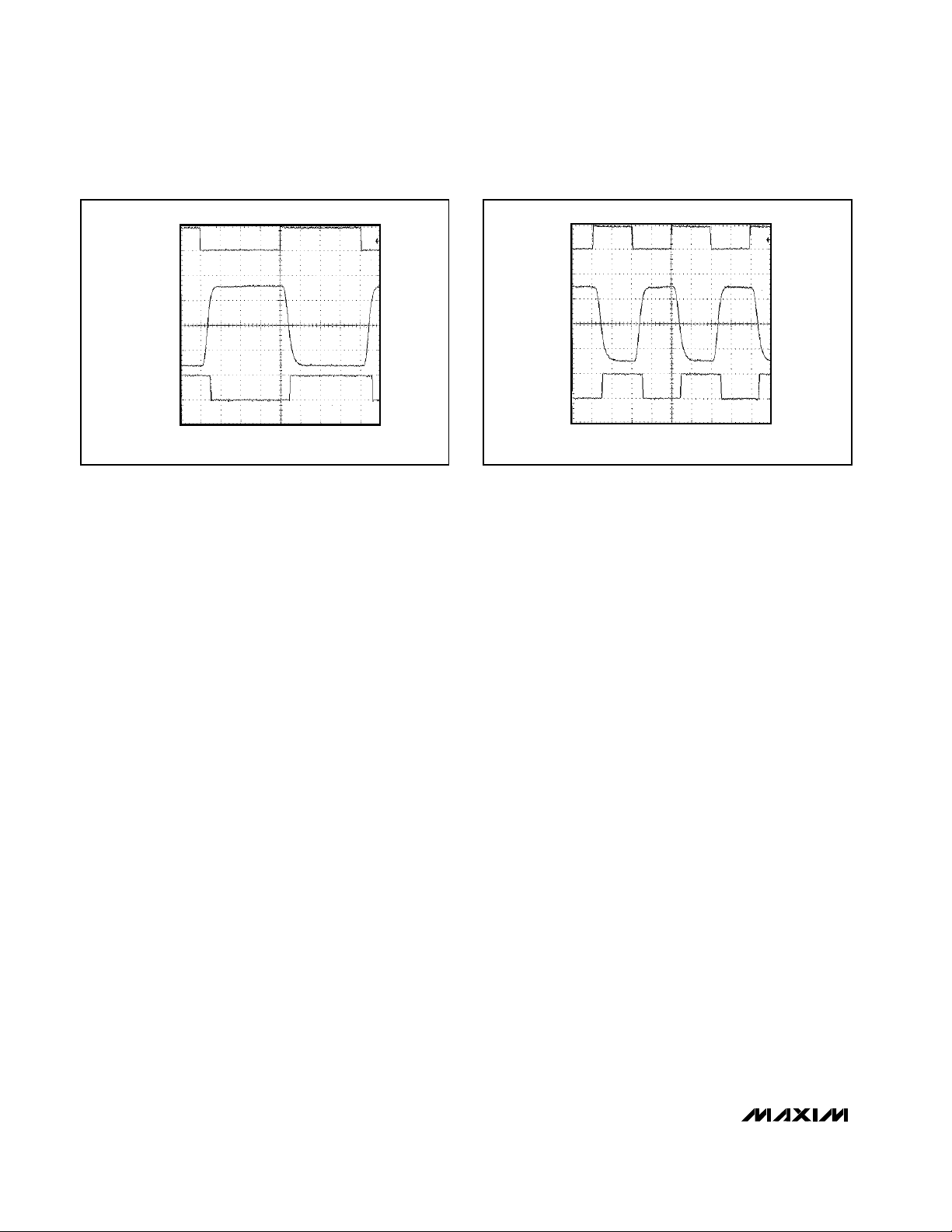
High Data Rates
The MAX221E maintains the RS-232 ±5.0V minimum
transmitter output voltage even at high data rates.
Figure 8 shows a transmitter loopback test circuit.
Figure 9 shows the loopback test result at 120kbps,
and Figure 10 shows the same test at 250kbps.
Figure 7. Transmitter Output when Exiting Shutdown or
Powering Up
Figure 8. Loopback Test Circuit
5V/div FORCEON =
TIN = GND
5V/div
TIN = V
50µs/div
FORCEOFF
TOUT
CC
+5V
0.1µF
C1+
C1
C2
0V
V
CC
C1-
C2+
C2-
TIN
ROUT
EN
FORCEOFF
FORCEON
MAX221E
V
GND
C3
CC
V+
V-
TOUT
RIN
5k
INVALID
C4
1000pF
MAX221E
±15kV ESD-Protected, +5V, 1µA, Single RS-232
Transceiver with AutoShutdown
10 ______________________________________________________________________________________
Figure 9. Loopback Test Result at 120kbps
Figure 10. Loopback Test Result at 250kbps
___________________Chip Information
TRANSISTOR COUNT: 157
5V/div
5V/div
5V/div
2µs/div
TIN
TOUT
ROUT
5V/div
5V/div
5V/div
2µs/div
TIN
TOUT
ROUT

MAX221E
±15kV ESD-Protected, +5V, 1µA, Single RS-232
Transceiver with AutoShutdown
______________________________________________________________________________________ 11
Package Information
TSSOP.EPS

MAX221E
±15kV ESD-Protected, +5V, 1µA, Single RS-232
Transceiver with AutoShutdown
Maxim cannot assume responsibility for use of any circuitry other than circuitry entirely embodied in a Maxim product. No circuit patent licenses are
implied. Maxim reserves the right to change the circuitry and specifications without notice at any time.
12
____________________Maxim Integrated Products, 120 San Gabriel Drive, Sunnyvale, CA 94086 408-737-7600
© 1999 Maxim Integrated Products Printed USA is a registered trademark of Maxim Integrated Products.
Package Information (continued)
SSOP.EPS
 Loading...