Page 1

General Description
The MAX2204 RF power detector is designed to operate from 450MHz to 2.5GHz. The device is ideal for
wideband code-division multiple access (WCDMA),
cdma2000
®
, and high-speed downlink/uplink packet
access. The MAX2204 accepts an RF signal at the
input, and outputs a highly repeatable voltage. The output voltage increases monotonically with increasing
input power. The device is designed to compensate for
temperature and process shifts, reducing the typical
output variation to less than ±0.5dB at full input power
and ±1.5dB at the lower power.
The MAX2204 features a detection range from -16dBm
to +5dBm. High input impedance allows for low-loss
resistive tap if an isolator is used. The device uses
external termination at the input so that the RF signal
from several directional couplers can be connected to
a single detector chip.
The MAX2204 operates from a 2.7V to 3.3V power
supply. The device is available in a tiny 5-pin SC70 package. Electrical performance is guaranteed over a -40°C to
+85°C temperature range.
Applications
WCDMA, cdma2000
High-Speed Downlink Packet Access (HSDPA)
High-Speed Uplink Packet Access (HSUPA)
Features
o -16dBm to +5dBm Detection Range
o ±0.3dB Detection Error Due to Temperature
o +2.7V to +3.3V Single-Supply Operation
o Easy-to-Assemble, Lead-Free, 5-Pin SC70
Package
MAX2204
RF Power Detector
________________________________________________________________
Maxim Integrated Products
1
Pin Configuration
Ordering Information
19-0753; Rev 0; 4/07
For pricing, delivery, and ordering information, please contact Maxim/Dallas Direct! at
1-888-629-4642, or visit Maxim’s website at www.maxim-ic.com.
+
Denotes a lead-free package.
cdma2000 is a registered trademark of Telecommunications
Industry Association.
EVALUATION KIT
AVAILABLE
PART TEMP RANGE
MAX2204EXK+ -40°C to +85°C 5 SC70 X5+1
PINPACKAGE
PKG
CODE
TOP VIEW
GND
+
1 5 OUTVCC
2
MAX2204
34
ENARFIN
Page 2

MAX2204
RF Power Detector
2 _______________________________________________________________________________________
ABSOLUTE MAXIMUM RATINGS
DC ELECTRICAL CHARACTERISTICS
(VCC= 2.7V to 3.3V, TA= -40°C to +85°C, ENA = 2.0V, no RF signal applied. Typical values are at VCC= 2.85V, TA= +25°C, unless
otherwise noted.) (Note 1)
Stresses beyond those listed under “Absolute Maximum Ratings” may cause permanent damage to the device. These are stress ratings only, and functional
operation of the device at these or any other conditions beyond those indicated in the operational sections of the specifications is not implied. Exposure to
absolute maximum rating conditions for extended periods may affect device reliability.
Note 1: Specifications over TA= -40°C to +85°C are guaranteed by design. Production tests are performed at TA= +25°C.
Note 2: Guaranteed by design and characterization.
V
CC
to GND ...........................................................-0.3V to +3.6V
OUT, Logic Input (ENA) to GND ................-0.3V to (V
CC
+ 0.3V)
RF Input Power ...............................................................+10dBm
Continuous Power Dissipation (T
A
= +70°C)
(derate 3.1mW/°C above +70°C)................................247mW
Operating Temperature Range ...........................-40°C to +85°C
Junction Temperature......................................................+150°C
θ
JC
...............................................................................+115°C/W
θ
JA
...............................................................................+324°C/W
Storage Temperature Range .............................-65°C to +160°C
Lead Temperature (soldering, 10s) .................................+300°C
PARAMETER SYMBOL CONDITIONS MIN TYP MAX UNITS
Supply Voltage VCC 2.7 3.3 V
Operating Supply Current ICC 1.2 2.5 mA
Sleep Mode Supply Current ENA = 0V 0.5 10 µA
ENA Logic-High Threshold VIH 2 V
ENA Logic-Low Threshold VIL 0.6 V
ENA = 2V -2 +10
ENA Input Current
ENA = 0.6V -2 +1
µA
AC ELECTRICAL CHARACTERISTICS
(MAX2204 Evaluation Kit, VCC= 2.85V, TA= -40°C to +85°C, ENA = 2.0V. fRF= 450MHz to 2.5GHz. Typical values are at VCC= 2.85V,
T
A
=+25°C, unless otherwise noted.) (Note 1)
Note: This part is not for automotive applications.
CAUTION! ESD SENSITIVE DEVICE
RF Input Frequency 450 2500 MHz
RF Input Level for 2.0V
Minimum Input Level
Power Detector Accuracy Due to
Temperature
In-Band Variation
PARAMETER SYMBOL CONDITIONS MIN TYP MAX UNITS
= +25°C, RFIN at 836MHz 3.3 4.8 6.3
T
A
T
= +25°C, RFIN at 1880MHz 1.9 3.4 4.9
A
-16dBm to -15dBm change in P
(836MHz to 2500MHz)
= 2.85V,
V
CC
836MHz to 1880MHz
= -40°C to +85°C
T
A
(Note 2)
824MHz to 849MHz 0.1
1850MHz to 1980MHz 0.2
IN
PIN for 2.0V output ±0.5 ±1.1
for 0.1V output ±1.5 ±4
P
IN
814 mV
dBm
dB
dB
Page 3
MAX2204
RF Power Detector
_______________________________________________________________________________________
3
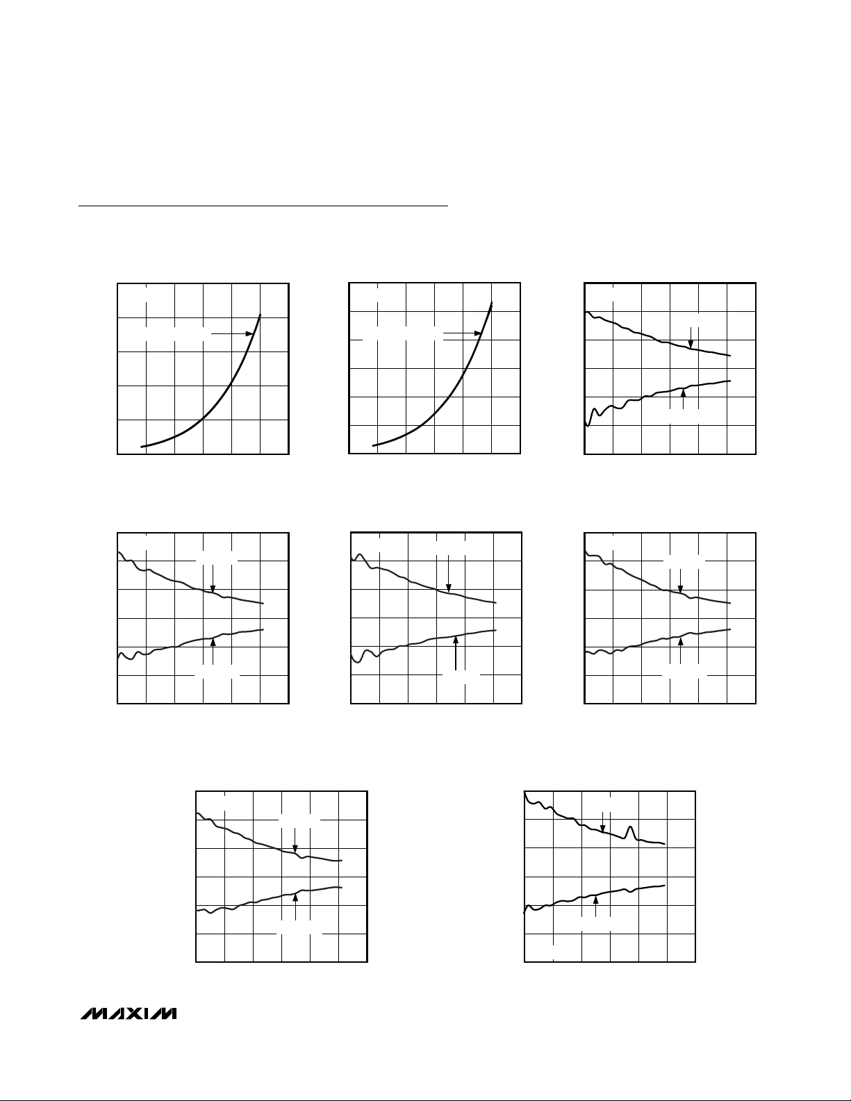
Typical Operating Characteristics
(MAX2204 Evaluation Kit, typical values are at VCC= 2.85V, ENA = 2.0V, TA= +25°C, modulation equals CW, unless otherwise noted.)
OUTPUT VOLTAGE vs. INPUT POWER
2.5
f = 836MHz
2.0
VCC = 2.7V, 3.0V, 3.3V
1.5
(V)
OUT
V
1.0
0.5
0
-20 -15 -10 -5 0 5 10
PIN (dBm)
DETECTOR ERROR FROM
= +25°C AT 824MHz
T
1.5
1.0
0.5
A
f = 824MHz
TA = -40°C
MAX2204 toc01
MAX2204 toc04
OUTPUT VOLTAGE vs. INPUT POWER
3.0
f = 1950MHz
2.5
VCC = 2.7V, 3.0V, 3.3V
2.0
(V)
1.5
OUT
V
1.0
0.5
0
-20 -15 -10 -5 0 5 10
PIN (dBm)
DETECTOR ERROR FROM
= +25°C AT 849MHz
T
f = 849MHz
A
TA = -40˚C
1.5
1.0
0.5
MAX2204 toc02
MAX2204 toc05
1.5
1.0
0.5
0
ERROR (dB)
-0.5
-1.0
-1.5
1.5
1.0
0.5
DETECTOR ERROR FROM
= +25°C AT 450MHz
T
A
f = 450MHz
TA = -40°C
TA = +85°C
-20 -15 -10 -5 0 5 10
PIN (dBm)
DETECTOR ERROR FROM
= +25°C AT 1850MHz
T
A
f = 1850MHz
TA = -40°C
MAX2204 toc03
MAX2204 toc06
0
ERROR (dB)
-0.5
-1.0
-1.5
-20 -15 -10 -5 0 5 10
TA = +85°C
PIN (dBm)
DETECTOR ERROR FROM
T
1.5
1.0
0.5
0
ERROR (dB)
-0.5
-1.0
-1.5
-20 -15 -10 -5 0 5 10
A
f = 1910MHz
ERROR (dB)
= +25°C AT 1910MHz
TA = -40°C
TA = +85°C
PIN (dBm)
0
-0.5
-1.0
-1.5
-20 -15 -10 -5 0 5 10
MAX2204 toc07
TA = +85˚C
PIN (dBm)
0
ERROR (dB)
-0.5
-1.0
-1.5
-20 -15 -10 -5 0 5 10
DETECTOR ERROR FROM
= +25°C AT 2500MHz
T
1.5
1.0
0.5
0
ERROR (dB)
-0.5
-1.0
-1.5
-20 -15 -10 -5 0 5 10
A
TA = -40°C
TA = +85°C
f = 2500MHz
PIN (dBm)
TA = +85°C
P
(dBm)
IN
MAX2204 toc08
Page 4

MAX2204
RF Power Detector
4 _______________________________________________________________________________________
Typical Operating Characteristics (continued)
(MAX2204 Evaluation Kit, typical values are at VCC= 2.85V, ENA = 2.0V, TA= +25°C, modulation equals CW, unless otherwise noted.)
OUTPUT VOLTAGE vs. INPUT POWER
AT 836MHz WITH RESISTIVE TAP
PIN (dBm)
V
OUT
(V)
MAX2204 toc09
0 5 10 15 20 25 30
0
0.5
1.0
1.5
2.0
2.5
f = 836MHz
R = 3kΩ
OUTPUT VOLTAGE vs. INPUT POWER
AT 1880MHz WITH RESISTIVE TAP
PIN (dBm)
V
OUT
(V)
MAX2204 toc10
0 5 10 15 20 25 30
0
0.5
1.0
1.5
2.0
2.5
f = 1880MHz
R = 1.5kΩ
200µs/div
RESPONSE TIME
MAX2204 toc11
V
OUT
200mV/div
ENA
1V/div
DEVIATION FROM DPCCH+1DPDCH, 1950MHz
PIN (dBm)
DEVIATION (dB)
MAX2204 toc12
-25 -20 -15 -10 -5 0 5 10
-0.6
-0.4
-0.2
0
0.2
0.4
0.6
DPCCH+5DPDCH
DPCCH+4DPDCH
DPCCH+3DPDCH
DPCCH+2DPDCH
f = 1950MHz
OUTPUT VOLTAGE vs. INPUT POWER
WITH WCDMA DOWNLINK
PIN (dBm)
V
OUT
(V)
MAX2204 toc13
-20 -15 -10 -5 0 5 10
0
0.5
1.0
1.5
2.0
2.5
1 DPCH
PCPCH + SCH
3 DPCH,
PCPCH + SCH + 1DPCH,
PCPCH + SCH + 3DPCH
f = 2140MHz
Page 5
MAX2204
RF Power Detector
_______________________________________________________________________________________ 5
Pin Description
Detailed Description
The MAX2204 RF power detector is designed to operate
from 450MHz to 2.5GHz. The device accepts an RF
signal at the input and outputs a highly repeatable voltage, which increases monotonically with increasing
input power. See the
Typical Operating Characteristics
.
The device is designed to compensate for temperature
and process shifts, reducing the typical output variation
to less than ±0.5dB at full input power and ±1.5dB at
the lower power.
The MAX2204 features a detection range from -16dBm
to +5dBm. High input impedance allows a for low-loss
resistive tap if an isolator is used. The device uses
external termination at the input so that the RF signal
from several directional couplers can be connected to
a single detector chip.
The MAX2204 features an enable input (ENA) that
allows the device to be put in shutdown. For normal
operation, drive ENA high or connect to V
CC
. For
device shutdown, drive ENA low.
The MAX2204 integrates an output series resistor of
approximately 100kΩ. For output filtering, connect only
a capacitor to ground at the output.
Applications Information
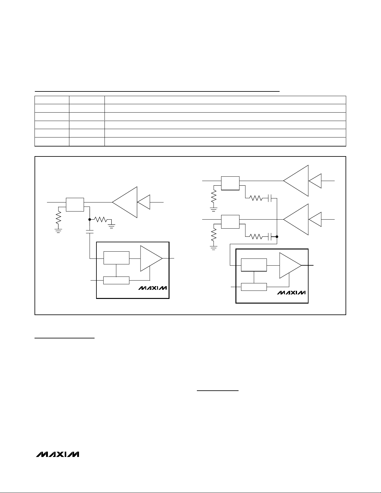
The MAX2204 uses external termination when using
directional couplers. See Figure 1 for the typical application circuit. The output of the detector is typically
connected to an ADC in cdma2000 or WCDMA powercontrol topology.
Figure 1. Typical Application Circuit
PIN NAME FUNCTION
1VCCPower-Supply Pin. Bypass to GND with a capacitor as close as possible to the pin.
2 GND Ground Connection. Use multiple ground vias to connect the GND pin to the ground plane.
3 RFIN RF Input. AC-couple with an external capacitor.
4 ENA Enable Input. Drive low to turn the part off. Drive high or connect to VCC to turn the part on.
5 OUT Power Detector Output. Filter with a capacitor to GND.
PA 1
COUPLER 1
PA 1
10Ω
10Ω
PEAK
DETECT
PA 2
BUFFER
50Ω
COUPLER 1
50Ω
PEAK
DETECT
BUFFER
DETECTOR
OUTPUT
50Ω
COUPLER 2
50Ω
DETECTOR
OUTPUT
ENABLE
BIAS
MAX2204
APPLICATION DIAGRAM FOR ONE PA
ENABLE
BIAS
MAX2204
APPLICATION DIAGRAM FOR TWO PAs
Page 6
MAX2204
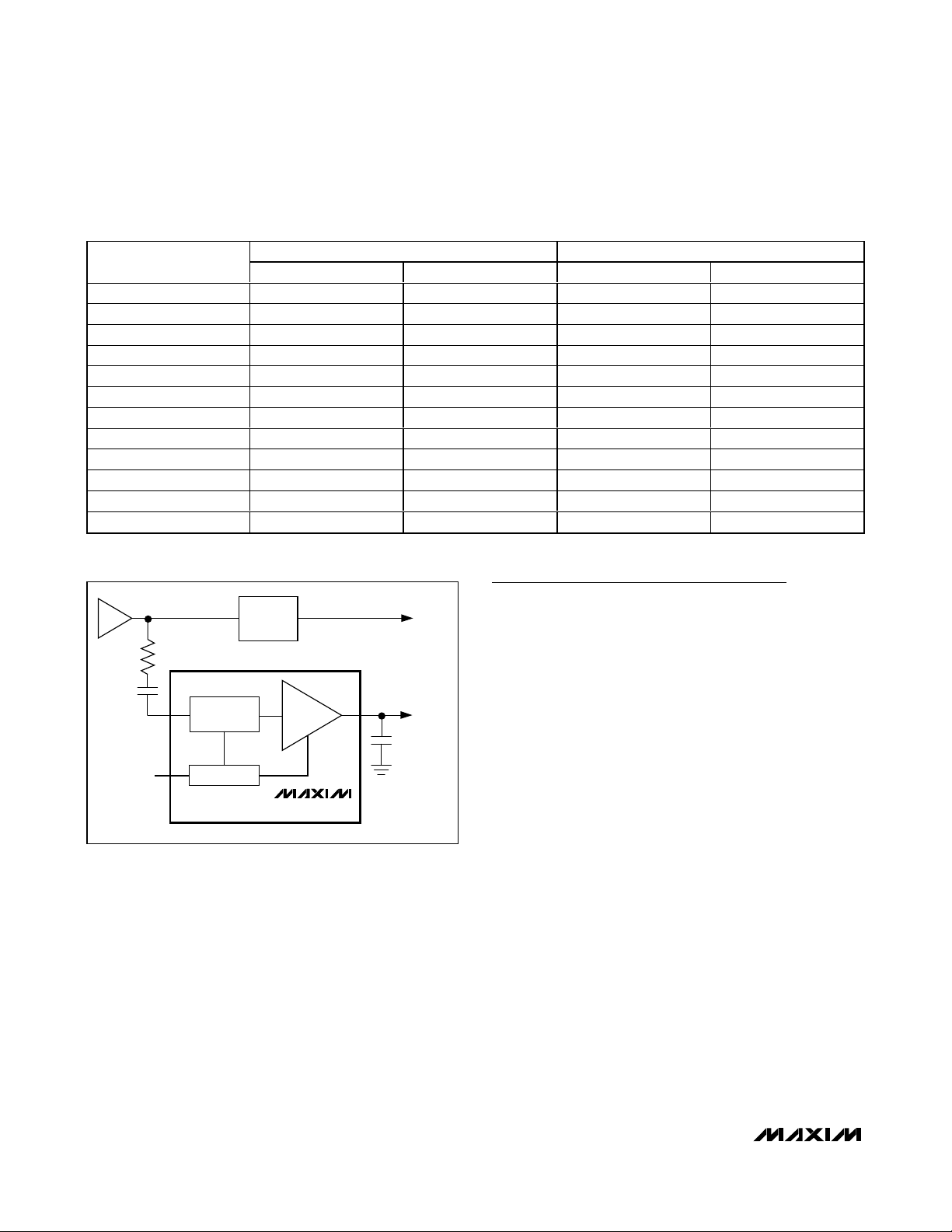
The MAX2204 has high input impedance to allow
for high-value resistive tapping from a power amplifier.
This coupling method is the lowest cost and lowest
power loss when used with an isolator. See Figure 2 for
the typical application circuit.
The MAX2204 input impedance over frequency is listed
in Table 1.
Layout
The MAX2204 is not particularly sensitive to the layout,
since it only needs 5dBm for maximum output voltage.
However, there are two areas that need attention: the
GND pin and the supply bypassing. The GND pin should
be connected to the PCB ground with a GND via as
close as possible, and the supply bypass capacitor
should be close to the part.
RF Power Detector
6 _______________________________________________________________________________________
Table 1. MAX2204 Input Impedance Over Frequency
Figure 2. Typical Application Circuit Using Resistive Tapping
from a Power Amplifier
FREQUENCY (GHz)
0.4 109.3 -556.5 120.0 -563.3
0.6 80.5 -369.0 91.0 -379.3
0.8 73.4 -300.3 80.8 -310.7
1.0 64.1 -260.2 75.6 -275.8
PA
1.2 65.8 -216.4 79.9 -231.3
1.4 62.3 -194.9 64.4 -202.8
1.6 48.9 -177.5 53.9 -192.3
1.8 33.1 -157.4 39.9 -174.6
2.0 21.8 -142.2 25.9 -158.3
2.2 15.2 -131.2 18.3 -144.5
2.4 10.6 -116.8 10.6 -131.9
2.6 11.8 -99.8 10.6 -115.6
PEAK
DETECT
REAL (Ω) IMAG (jΩ) REAL (Ω) IMAG (jΩ)
ISOLATOR
BUFFER
PIN = -16dBm PIN = +5dBm
TO ANT
OUTPUT
TO ADC
C
FILTER
ENABLE
BIAS
MAX2204
Page 7
MAX2204
RF Power Detector
Maxim cannot assume responsibility for use of any circuitry other than circuitry entirely embodied in a Maxim product. No circuit patent licenses are
implied. Maxim reserves the right to change the circuitry and specifications without notice at any time.
Maxim Integrated Products, 120 San Gabriel Drive, Sunnyvale, CA 94086 408-737-7600 _____________________
7
© 2007 Maxim Integrated Products is a registered trademark of Maxim Integrated Products, Inc.
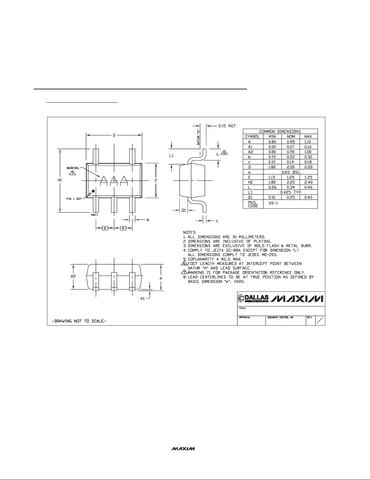
Package Information
(The package drawing(s) in this data sheet may not reflect the most current specifications. For the latest package outline information
go to www.maxim-ic.com/packages
.)
SC70, 5L.EPS
PACKAGE OUTLINE, 5L SC70
21-0076
1
E
1
 Loading...