

Page 1

General Description
The MAX2165 direct-conversion tuner IC is designed for
handheld digital video broadcast (DVB-H) applications.
The tuner covers a 470MHz to 780MHz input frequency
range and features an I/Q baseband interface.
The MAX2165’s direct-conversion architecture eliminates the need for an IF-SAW filter, allowing for
reduced bill of materials cost. The design integrates a
variable-gain, low-noise amplifier (LNA); a notch filter;
an RF tracking filter; a quadrature mixer; a power
detector; programmable baseband lowpass channelselection filters; baseband variable-gain amplifiers
(VGA); DC offset correction circuitry; and a complete
fractional-N frequency synthesizer. The part is programmable through a 2-wire I2C-compatible serial interface.
The MAX2165 integrates a tuneable notch filter. This filter is designed to notch out interfering signals in the
830MHz to 950MHz frequency range to allow for operation in the presence of large cellular signals.
Programmable baseband channel-selection filters allow
for operation with 7MHz and 8MHz channels. Digital DC
offset correction circuitry supports time-sliced operation
by minimizing power-up time delay. The fractional-N
synthesizer reduces VCO lock time and minimizes
close-in phase noise, eliminating the need for powerhungry, phase-noise reduction algorithms.
The MAX2165 is available in a tiny, 5mm x 5mm x
0.8mm, 28-pin thin QFN package with an exposed paddle. It is specified for operation over the -40°C to +85°C
extended temperature range.
Applications
DVB-H Handheld Receivers
DVB-T Portable Devices
DMB-T/H Portable Devices
ISDB-T Receivers (13 Segment)
Features
o 93mA (typ) Current Consumption from a Single
+2.85V Supply Voltage
o 21mW (typ) Average Power Consumption at 8%
Duty Cycle
o Direct-Conversion Architecture Eliminates IF-
SAW Filter
o Integrated RF Tuneable Notch Filter for Operation
in the Presence of Cellular Blockers
o Integrated DC Offset Correction Circuitry
o Integrated RF Notch Filter for Operation in the
Presence of Up to -7dBm Cellular Blockers
o Extended UHF Band Operation
o 5mm x 5mm x 0.8mm, 28-Pin Thin QFN Package
MAX2165
Single-Conversion DVB-H Tuner
________________________________________________________________
Maxim Integrated Products
1
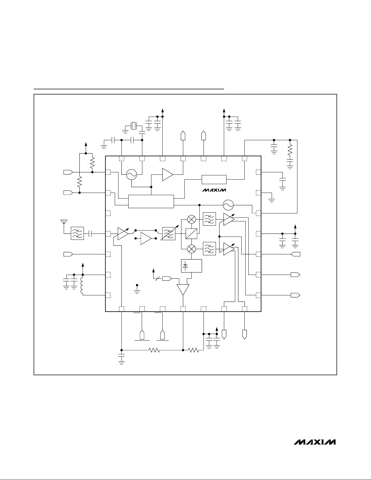
Pin Configuration/
Functional Diagram
Ordering Information
19-0646; Rev 1; 3/09
For pricing, delivery, and ordering information, please contact Maxim Direct at 1-888-629-4642,
or visit Maxim’s website at www.maxim-ic.com.
+
Denotes a lead(Pb)-free/RoHS-compliant package.
*
EP = Exposed paddle.
EVALUATION KIT
AVAILABLE
PART TEMP RANGE PIN-PACKAGE
MAX2165ETI+ -40°C to +85°C 28 TQFN-EP*
XB
VCC_XTAL
REFOUT
MUX
VCC_SYN
SDA
SCL
N.C.
RFIN
ADDR
VCC_RF
LEXT
XE
28 27 26 25 24 23 22
+
1
SERIAL INTERFACE, CONTROL,
2
3
4
5
6
7
AND SYNTHESIZER
MAX2165
TO
CONTROL
BLOCK
DAC
EP
0°
90°
PWRDET
CHARGE
PUMP
CP
21
LDO
20
GND_TUNE
19
VTUNE
18
VCC_VCO
17
BB_AGC
16
BBI+
15
BBI-
8 9 10 11 12 13 14
STBY
SHDN
RF_AGC
THIN QFN
5mm x 5mm
OVLD_DET
VCC_BB
BBQ-
BBQ+
Page 2
MAX2165
Single-Conversion DVB-H Tuner
2 _______________________________________________________________________________________
ABSOLUTE MAXIMUM RATINGS
DC ELECTRICAL CHARACTERISTICS
(MAX2165 EV kit, VCC= +2.75V to +3.3V, V
RF_AGC
= V
BB_AGC
= 2.3V (maximum gain), no RF input signals at RFIN, default register set-
tings, T
A
= -40°C to +85°C, unless otherwise noted. Typical values are at VCC= +2.85V, TA= +25°C, unless otherwise noted.) (Note 1)
AC ELECTRICAL CHARACTERISTICS
(MAX2165 EV kit, VCC= +2.75V to +3.3V, V
RF_AGC
= V
BB_AGC
= 2.3V (maximum gain), V
OUT
= 1V
P-P
, 75Ω system impedance, reg-
isters set according to the specified default register conditions, T
A
= -40°C to +85°C, unless otherwise noted. Typical values are at
V
CC
= +2.85V, TA= +25°C, unless otherwise noted.) (Note 1)
Stresses beyond those listed under “Absolute Maximum Ratings” may cause permanent damage to the device. These are stress ratings only, and functional
operation of the device at these or any other conditions beyond those indicated in the operational sections of the specifications is not implied. Exposure to
absolute maximum rating conditions for extended periods may affect device reliability.
All VCCPins to GND ..............................................-0.3V to +3.6V
GND_TUNE to GND ..............................................-0.3V to +0.3V
All Other Pins to GND.................................-0.3V to (V
CC
+ 0.3V)
BBI_, BBQ_ Short Circuit to Ground Duration ...............Indefinite
Maximum RF Input Power ..............................................+13dBm
Continuous Power Dissipation (T
A
= +70°C)
28-Pin Thin QFN (derate 34.5mW/°C above +70°C).....2758mW
Operating Temperature Range ...........................-40°C to +85°C
Junction Temperature......................................................+150°C
Storage Temperature Range .............................-65°C to +150°C
Lead Temperature (soldering, 10s) .................................+300°C
CAUTION! ESD SENSITIVE DEVICE
PARAMETER CONDITIONS MIN TYP MAX UNITS
SUPPL Y VOLTAGE AND CURRENT
Supply Voltage 2.75 3.30 V
Supply Current
Shutdown Current 20 µA
Gain-Control Voltage Required to obtain full range of RF and baseband gain 0.4 2.3 V
RF_AGC and BB _AGC Input
Bias Current
SERIAL INTERFACE
Input Logic-Leve l Low
Input Logic-Leve l High
Input Hysteres is
SDA, SCL Input Current -10 +10 µA
Output Logic-Leve l Low I
Output Logic-Leve l H igh I
LNASW = 1 (RF LNA on) 109 134
LNASW = 0 (RF LNA off) 93 116
V
AGC
SINK
SOURCE
at +0.4V and +2.3V -50 +50 µA
= 0.3mA 0.4 V
= 0.3mA
0.3 x
V
CC
0.7 x
V
CC
V
CC
0.4
-
V
0.05 x
V
CC
V
V
mA
V
OVERALL PERFORMANCE (RF INPUT TO BASEBAND OUTPUTS)
Operating Frequency Range
Input Return Loss
PARAMETER CONDITIONS MIN TYP MAX UNITS
Meets specified performance 470 783
Operates with derated performance (Note 2) 470 832
50Ω system, w or st case acr oss b and , any g ai n- contr ol
setti ng ( N ote 3)
7dB
MHz
Page 3
MAX2165
Single-Conversion DVB-H Tuner
_______________________________________________________________________________________ 3
AC ELECTRICAL CHARACTERISTICS (continued)
(MAX2165 EV kit, VCC= +2.75V to +3.3V, V
RF_AGC
= V
BB_AGC
= 2.3V (maximum gain), V
OUT
= 1V
P-P
, 75Ω system impedance, reg-
isters set according to the specified default register conditions, T
A
= -40°C to +85°C, unless otherwise noted. Typical values are at
V
CC
= +2.85V, TA= +25°C, unless otherwise noted.) (Note 1)
Voltage Gain
RF Gain-Control Range 0.4V ≤ V
Baseband Gain-Control Range 0.4V ≤ V
LNA Gain Step
LNA Gain Step Phase Change
Noise Figure (Note 3)
Input IP2 (Note 4)
Input IP3 (Note 5)
In-Band Input P
Cellular Blocker Desensitization
(Note 7)
In-Band IM3
RF Beats Converted to Output
RF Isolation
I/Q Output Swing Z
I/Q DC Voltage I+, I-, Q+, Q- outputs to ground VCC / 2 V
I/Q Quadrature Accuracy
Spurious Emissions at RF Input
(Note 3)
Closed-Loop Phase Noise
PARAMETER CONDITIONS MIN TYP MAX UNITS
1dB
Z
SOURCE
1kΩ
Gain change caused by switching RF LNA on (LNASW =
1) and off (LNASW = 0)
Phase change caused by switching RF LNA on (LNASW
= 1) and off (LNASW = 0)
At 470MHz 3.8 6.5
At 783MHz 4.0 6.5
Maximum gain 0 9
23dB gain reduction 26
Maximum gain -20 -4
23dB gain reduction 17
Maximum gain (Note 6)
Cellular Tx blocker gain compression 1.2 3
Cellular Tx blocker noise figure rise 3
Two tones (782.8MHz and 782.3MHz) within passband of
baseband filter, 780MHz LO frequency
170MHz to 960MHz RF input frequency < -60
960MHz to 1400MHz RF input frequency < -60
DC to 50MHz, RF input to baseband outputs relative to
desired channel
= 10kΩ || 10pF 0.5 1 V
LOAD
Phase error 2 degrees
Amplitude error -1.5 +1.5 dB
50MHz to 470MHz -38 -33
470MHz to 878MHz -52 -35
878MHz to 1732MHz -49 -35
Spur at four times Rx frequency, tested at f
= 1896MHz
f
SPUR
1kHz offset to 10kHz (Note 3) -86 -96
1MHz offset (Note 3) -108 -126
> 10MHz offset -140
= 75Ω, Z
≤ 2.3V 29
RF_AGC
≤ 2.3V 21 25 dB
BB_AGC
Maximum gain 74 82
>
LOAD
Minimum gain on
(LNASW = 1)
= 474MHz,
LO
23 29
34
13.5 17 dB
10 degrees
-22 dBm
-55 -40 dBc
-60 dBc
-58 -51 dBm
dB
dB
dB
dBm
dBm
dB
dBc
P-P
dBmV
dBc/Hz
Page 4
MAX2165
Single-Conversion DVB-H Tuner
4 _______________________________________________________________________________________
AC ELECTRICAL CHARACTERISTICS (continued)
(MAX2165 EV kit, VCC= +2.75V to +3.3V, V
RF_AGC
= V
BB_AGC
= 2.3V (maximum gain), V
OUT
= 1V
P-P
, 75Ω system impedance, reg-
isters set according to the specified default register conditions, T
A
= -40°C to +85°C, unless otherwise noted. Typical values are at
V
CC
= +2.85V, TA= +25°C, unless otherwise noted.) (Note 1)
Power-Up Time
BASEBAND FILTERS
PARAMETER CONDITIONS MIN TYP MAX UNITS
Shutdown to full operation, VCO settled to the Rx
frequency, DC offset calibrated (Note 8)
Lower corner (Note 9)
Passband Cutoff Attenuation
Amplitude Ripple TA = +25°C 0.5 1.5 dB
Group Delay Ripple 150 µs
Group Delay Matching 5ns
Rejection Ratio (Note 10)
FRACTIONAL SYNTHESIZER
RF N-Divider Ratio 7 251
RF R-Divider Ratio 12
Fractional Ratio Length of fractional accumulator (Note 13) 20 bits
Integer Spurs Worst-case spur inside baseband filter bandwidth -60 dBc
Settling Time
Charge-Pump Current
Charge-Pump Leakage -10 +10 µA
REFERENCE OSCILLATOR
Reference Frequency 4 26 MHz
Reference Buffer Output Voltage
Swing
Input Impedance
Input Voltage
OVERLOAD DETECTOR
Attack-Point Accuracy ±2.5 dB
Attack-Point Increment 3-bit DAC, change per LSB step 2.5 dB
Detector Output Sink
Upper corner at 3.85MHz (UHF mode), TA = +25°C 0.9 5
Upper corner at 3.35MHz (VHF mode), T
4.75MHz (VHF mode) (Note 11) 23
5.25MHz (UHF mode) (Note 11) 23
14.5MHz (VHF and UHF mode) (Note 12) 59 75
> 16.2MHz 84
35MHz step, settled to within 100Hz frequency error / 20°
phase error
ICP = 0 0.6
ICP = 1 1.2
10kΩ || 10pF load 0.5 1 V
When used as a passive input for an external reference
oscillator
When used as a passive input for an external reference
oscillator
Detector on 0.1 mA
Detector off 5 µA
= +25°C 2.7 5
A
< 1 20 ms
0 or
200
200 µs
12 kΩ
100 600 mV
Hz
dB
P-P
P-P
dB
mA
P-P
RMS
Page 5
MAX2165
Single-Conversion DVB-H Tuner
_______________________________________________________________________________________ 5
AC ELECTRICAL CHARACTERISTICS (continued)
(MAX2165 EV kit, VCC= +2.75V to +3.3V, V
RF_AGC
= V
BB_AGC
= 2.3V (maximum gain), V
OUT
= 1V
P-P
, 75Ω system impedance, reg-
isters set according to the specified default register conditions, T
A
= -40°C to +85°C, unless otherwise noted. Typical values are at
V
CC
= +2.85V, TA= +25°C, unless otherwise noted.) (Note 1)
Note 1: Min and max limits are guaranteed by test at TA= +25°C and are guaranteed by design and characterization at TA=
-40°C and +85°C. The default register settings are not production tested. Load registers no sooner than 100µs after
power-up.
Note 2: Notch filter must be disabled by programming the TF_NTCH[3:0] bits to 1111 to enable operation up to 832MHz. Under
extreme conditions, the part can experience up to 3dB degradation in sensitivity and intermodulation distortion.
Note 3: Guaranteed by design and characterization over the specified operating conditions. Not production tested.
Note 4: UHF tones resulting in f
1
- f2beat frequency within the baseband output. Two tones at 350MHz and 1133MHz
with IM2 measured at 783MHz.
Note 5: Two tones converted to 5.25MHz and 10.75MHz, IM3 measured at 250kHz.
Note 6: A desired signal at P
DESIRED
= -78dBm is injected and downconverted to 3.75MHz. A blocker tone is injected at 10MHz
higher in frequency. Specified level is blocker power at which desired output signal compresses by 1dB. T
A
= +25°C.
Note 7: A single blocker at -7dBm with a bandwidth of less than 4MHz is injected at 880MHz with the receiver tuned to 783MHz
and set to maximum gain.
Note 8: VCO locked to within 100Hz of the Rx frequency. Wake-up initiated by toggling the SHDN pin from low to high and con-
necting the STBY pin to ground.
Note 9: Applies to continuous DC correction operation (DVB-T mode). In DVB-H mode, optional correction hold feature allows
quasi-DC-coupling.
Note 10: Depends on 7MHz/8MHz bandwidth mode.
Note 11: Equivalent to video carrier in upper adjacent channel. T
A
= +25°C.
Note 12: Equivalent to f
NYQUIST
- 3.8MHz for 18.3MHz sampling rate baseband DAC.
Note 13: Total frequency resolution is f
REF
/ 220, or approximately 20Hz with a 20MHz reference frequency.
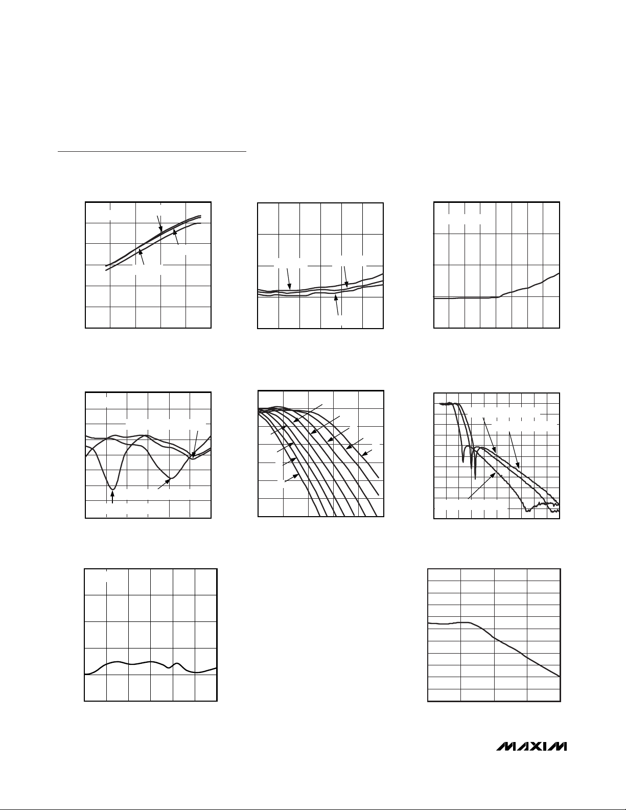
Typical Operating Characteristics
(MAX2165 EV kit, VCC= +2.85V, default register settings, V
RF_AGC
= V
BB_AGC
= 2.3V, V
IOUT
= V
QOUT
= 500mV
P-P
, TA= +25°C,
unless otherwise noted.)
SUPPLY CURRENT vs. SUPPLY VOLTAGE
VCC (V)
I
CC
(mA)
MAX2165 toc01
2.6 2.8 3.0 3.2 3.4
100
105
110
115
120
TA = -40°C
TA = +85°C
TA = +25°C
VOLTAGE GAIN vs. FREQUENCY
FREQUENCY (MHz)
GAIN (dB)
MAX2165 toc02
470 535 600 665 730 795 860
65
70
75
80
85
90
95
100
TA = -40°C
TA = +85°C
TA = +25°C
VOLTAGE GAIN vs. RFAGC
MAX2165 toc03
2.01.51.00.5
40
50
60
70
80
90
30
0 2.5
TA = +85°C
TA = -40°C
TA = +25°C
BB_AGC = 2.3V
GAIN (dB)
RF_AGC CONTROL VOLTAGE (V)
PARAMETER CONDITIONS MIN TYP MAX UNITS
Detector Gain 150 V/V
Detector Response Time 5µs
2-WIRE SERIAL INTERFACE
Clock Rate I2C fast mode, slave category 400 kHz
Page 6
MAX2165
Single-Conversion DVB-H Tuner
6 _______________________________________________________________________________________
PHASE
NOISE
(dB
/H
)
Typical Operating Characteristics (continued)
(MAX2165 EV kit, VCC= +2.85V, default register settings, V
RF_AGC
= V
BB_AGC
= 2.3V, V
IOUT
= V
QOUT
= 500mV
P-P
, TA= +25°C,
unless otherwise noted.)
VOLTAGE GAIN vs. BBAGC
90
RF_AGC = 2.3V
80
70
60
GAIN (dB)
50
40
30
0 0.5 1.0 1.5 2.0 2.5
BB_AGC CONTROL VOLTAGE (V)
TA = -40°C
MAX2165 toc04
TA = +25°C
TA = +85°C
NOISE FIGURE (dB)
NOISE FIGURE vs. FREQUENCY
12
9
TA = +85°C
6
3
0
470 535 600 665 730 795 860
TA = +25°C
TA = -40°C
FREQUENCY (MHz)
MAX2165 toc05
NOISE FIGURE vs. RF Tx INPUT POWER
20
BLOCKER AT 880MHz
15
10
NOISE FIGURE (dB)
5
0
-22.5-25.0 -20.0
-17.5
RF Tx INPUT POWER (dBm)
-12.5-15.0
-10.0
MAX2165 toc06
-7.5 -5.0
RF INPUT RETURN LOSS
vs. FREQUENCY
0
ZO = 75Ω
5
10
15
20
25
RETURN LOSS (dB)
30
35
TRACKING FILTER SETTING "7"
40
TRACKING FILTER SETTING "1"
TRACKING FILTER SETTING "15"
FREQUENCY (MHz)
PHASE NOISE vs. RF FREQUENCY
-60
10kHz OFFSET
-70
z
m
-80
-90
-100
-110
470 535 600 665 730 795 860
RF FREQUENCY (MHz)
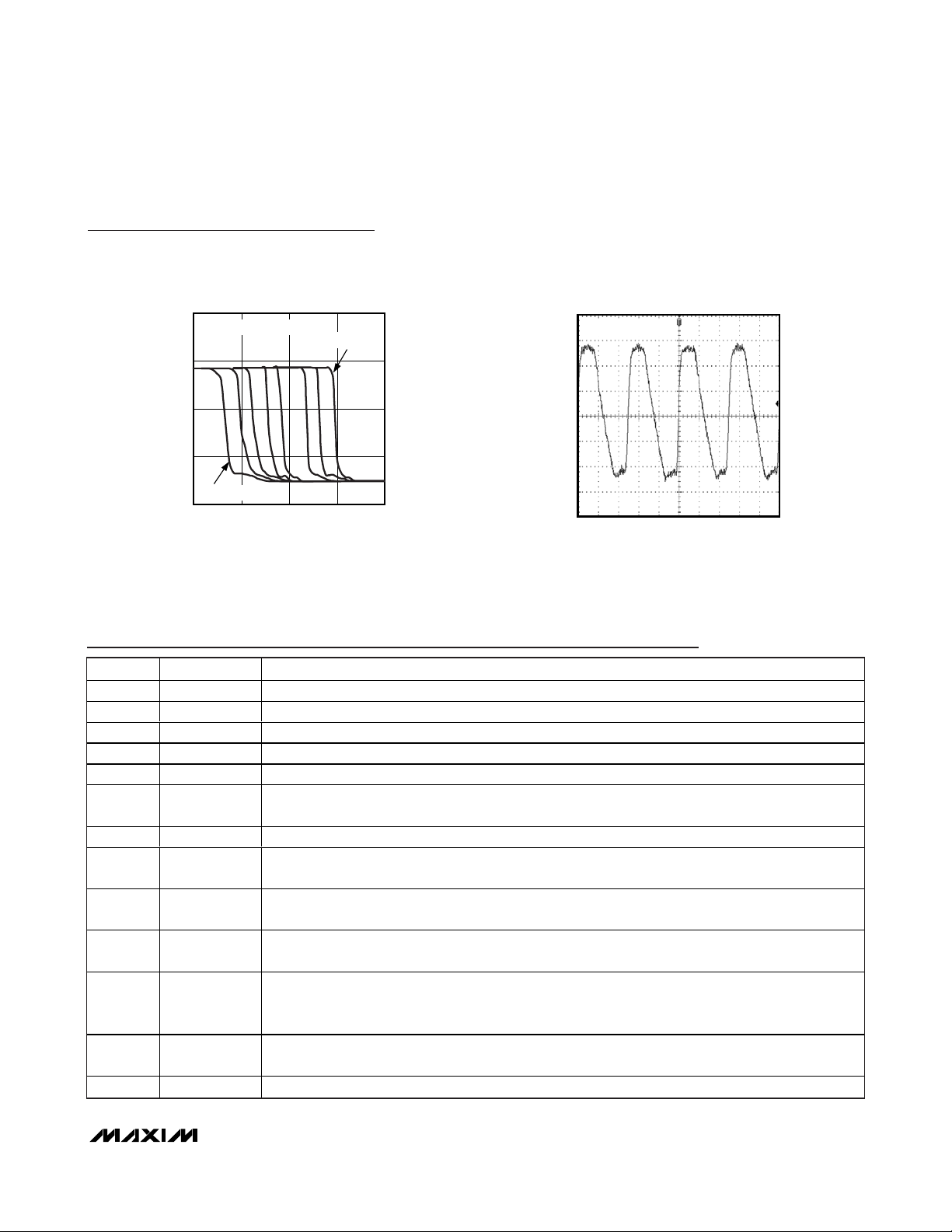
NORMALIZED BASEBAND
FREQUENCY RESPONSE
5
MAX2165 toc07
860
795730665600535470
0
-5
-10
-15
GAIN (dB)
-20
-25
-30
3.0 3.5 4.0 4.5 5.0 5.5
A: +2 ADJUSTMENT FACTOR
B: +1 ADJUSTMENT FACTOR
C: 0 ADJUSTMENT FACTOR
D: -1 ADJUSTMENT FACTOR
E: -2 ADJUSTMENT FACTOR
MAX2165 toc10
F
G
H
I
E
FREQUENCY (MHz)
F: -3 ADJUSTMENT FACTOR
G: -4 ADJUSTMENT FACTOR
H: -5 ADJUSTMENT FACTOR
I: -6 ADJUSTMENT FACTOR
D
C
B
A
A
MAX2165 toc08
10.0
0
-10.0
-20.0
-30.0
-40.0
-50.0
GAIN (dB)
-60.0
-70.0
-80.0
-90.0
-100.0
-110.0
-50
-60
-70
NORMALIZED BASEBAND
FREQUENCY RESPONSE
+0 ADJUSTMENT FACTOR
+2 ADJUSTMENT FACTOR
-6 ADJUSTMENT FACTOR
02 4 20
86
1210
FREQUENCY (MHz)
1816
14
PHASE NOISE vs. OFFSET FREQUENCY
MAX2165 toc09
MAX2165 toc11
-80
-90
-100
-110
-120
-130
PHASE NOISE (dBm/Hz)
-140
-150
-160
1 10 100 1000 10,000
OFFSET FREQUENCY (kHz)
Page 7
MAX2165
Single-Conversion DVB-H Tuner
_______________________________________________________________________________________ 7
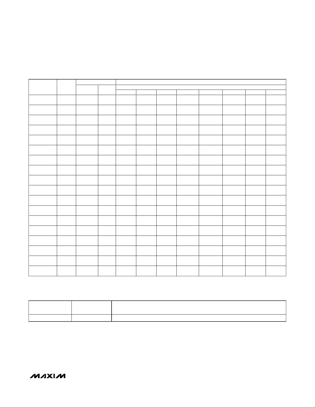
Typical Operating Characteristics (continued)
(MAX2165 EV kit, VCC= +2.85V, default register settings, V
RF_AGC
= V
BB_AGC
= 2.3V, V
IOUT
= V
QOUT
= 500mV
P-P
, TA= +25°C,
unless otherwise noted.)
REFERENCE BUFFER OUTPUT SIGNAL
MAX2165 toc13
200mV/div
20ns/div
10kΩ || 10pF LOAD
Pin Description
POWER-DETECTOR OUTPUT VOLTAGE
4
3
2
1
POWER-DETECTOR OUTPUT VOLTAGE (V)
0
-70
vs. RF INPUT POWER
40kΩ PULLUP TO 2.85V
PD_TH[2:0] = 000
-60
RF INPUT POWER (dBm)
PD_TH[2:0] = 111
-50 -40
MAX2165 toc12
-30
PIN NAME FUNCTION
1 SDA Serial-Data Input/Output. Requires a pullup resistor to VCC.
2 SCL Serial-Clock Input. Requires a pullup resistor to VCC.
3 N.C. No Connection. Connect this pin to ground.
4 RFIN RF Input. Internally matched to 75Ω. Requires a DC-blocking capacitor.
5 ADDR Address-Select Input. Selects the I2C slave address. See Table 20.
6 VCC_RF
RF Power-Supply Input. Connect to a low-noise, power-supply voltage. Bypass to the PCB ground
plane with a 2200pF and 100nF capacitor placed as close as possible to the pin.
7 LEXT External Inductor Connection. Connect to V
8 RF_AGC
9 SHDN
10 STBY
11 OVLD_DET
12 VCC_BB
RF Gain-Control Voltage Input. Accepts voltages from 0.4V to 2.3V with 2.3V providing maximum RF
gain. This pin can also be controlled by the OVLD_DET output. See the Typical Application Circuit.
Shutdown Input. Drive this pin low to disable all internal circuits and to put the device into low-power
shutdown mode. Drive this pin high for normal operation.
Standby Input. Controls the power-up sequence of the chip. See the Power-Up Sequence section for
more information on this pin’s operation.
Overload-Detection Output. This output provides an error signal between the internal power-detector
output voltage and an internal programmable reference voltage. This output can be connected to the
RF_AGC input to implement a closed RF automatic gain-control loop.
Baseband Power-Supply Input. Connect to a low-noise power-supply voltage. Bypass to the PCB
ground plane with a 1000pF and 100nF capacitor placed as close as possible to the pin.
13 BBQ- Inverting Quadrature Baseband Output
with a 39nH inductor.
CC
Page 8

MAX2165
Detailed Description
Register Descriptions
The MAX2165 includes 15 programmable registers and
three read-only registers. See Table 1 for register configurations. The register configuration of Table 1 shows
each bit name and the bit usage information for all registers. U labeled under each bit name indicates that the
bit value is user defined to meet specific application
requirements. A 0 or 1 indicates that the bit must be set
to the defined 0 or 1 value for proper operation.
Operation is not tested or guaranteed if these bits are
programmed to other values and is only for
factory/bench evaluation. In typical application, always
program to the operation defined state.
See Tables 2–19 for detailed descriptions of each register. All registers must be written 100µs after power-up
and no earlier than 100µs after power-up.
Single-Conversion DVB-H Tuner
8 _______________________________________________________________________________________
Pin Description (continued)
PIN NAME FUNCTION
14 BBQ+ Noninverting Quadrature Baseband Output
15 BBI- Inverting In-Phase Baseband Output
16 BBI+ Noninverting In-Phase Baseband Output
17 BB_AGC
18 VCC_VCO
19 VTUNE VCO Tuning Voltage Input. Connect to the PLL loop filter output.
20 GND_TUNE VCO Tuning Voltage Ground. Connect to the PCB ground plane.
21 LDO
22 CP Charge-Pump Output. Connect to the PLL loop filter input.
23 VCC_SYN
24 MUX
Baseband Gain-Control Voltage Input. Accepts voltages from 0.4V to 2.3V with 2.3V providing the
maximum baseband gain.
VCO Power-Supply Input. Connect to a low-noise power-supply voltage. Bypass to the PCB ground
plane with a 1000pF and 100nF capacitor placed as close as possible to the pin.
VCO Linear-Regulator Noise Bypass. Bypass to the PCB ground plane with a 470nF capacitor placed
as close as possible to the pin.
Synthesizer Power-Supply Input. Connect to a low-noise power-supply voltage. Bypass to the PCB
ground plane with a 1000pF and 100nF capacitor placed as close as possible to the pin.
Multiplexed Output Line. Output for various test functions, can also be used as a PLL lock-detect
indicator. See Table 9 for more information. When used as a PLL lock detector, logic-high indicates
PLL is not locked and logic-low indicates PLL is locked.
25 REFOUT
26 VCC_XTAL
27 XB
28 XE
EP EP Exposed Paddle. Solder evenly to the board’s ground plane to achieve the lowest impedance path.
Reference Buffer Output. Provides a buffered crystal-oscillator signal that can be used as a clock
reference for the demodulator. Requires a DC-blocking capacitor.
Crystal-Oscillator Power-Supply Input. Connect to a low-noise power-supply voltage. Bypass to the
PCB ground plane with a 1000pF and 100nF capacitor placed as close as possible to the pin.
Reference Input. Connect to a parallel resonant mode crystal through a load-matching capacitor or to
a reference oscillator.
Reference-Oscillator Feedback Input. Connect to a capacitive feedback network when the on-chip
reference oscillator is used. Leave unconnected when an external reference is used.
Page 9
MAX2165
Single-Conversion DVB-H Tuner
_______________________________________________________________________________________ 9
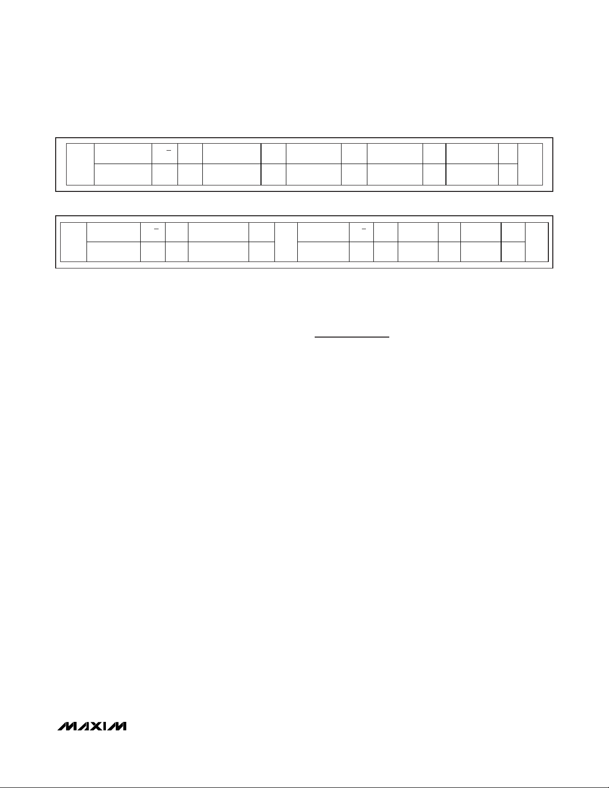
Table 1. Register Configuration*
Table 2. N-Divider Integer Register (Address: 0x00)
*
See the Register Descriptions section for more information on recommended settings.
REGISTER
NAME
N-Divider Integer 0x00 — H17
N-Divider Frac2 0x01 — H18
N-Divider Frac1 0x02 — H00
N-Divider Frac0 0x03 — H00
Tracking Filter 0x04 — H72
LNA 0x05 — H01
PLL
Configuration
Test 0x07 — H08
Shutdown 0x08 — H00
VCO Control 0x09 — H50
Baseband
Control
DC Offset Control 0x0B H79 H71
DC Offset DAC 0x0C H00 H00
ROM Table
Address
Reserved 0x0E H00 H00
ROM Table Data
Readback
Chip Status
Readback
Autotuner
Readback
REGISTER
ADDRESS
0x06 — H0A
0x0A — HF3
0x0D — H00
0x10 N/A N/A TRF7 TRF6 TRF5 TRF4 TRF3 TRF2 TRF1 TRF0
0x11 N/A N/A POR VASA VASE LD DC_LO DC_HI X PD_OVLD
0x12 N/A N/A VCO1 VCO0 BS2 BS1 BS0 ADC2 ADC1 ADC0
REGISTER SETTINGS MSB LSB
OPERATION
DEFINED
DEFAULT
(POR)
D7 D6 D5 D4 D3 D2 D1 D0
N7
U
X
0
F15
U
F7
U
TF_NTCH3UTF_NTCH2UTF_NTCH1UTF_NTCH0UTF_BAL3
X
0
RDIV
U
CP_TST20CP_TST10CP_TST0
X
0
VCO1
U
BB_BW3UBB_BW2UBB_BW1UBB_BW0UBB_BIA0
X
0
DC_DAC70DC_DAC60DC_DAC50DC_DAC40DC_DAC30DC_DAC20DC_DAC10DC_DAC0
X
0
X
0
N6
U
X
0
F14
U
F6
U
X
0
ICP
U
SHDN_REF
U
VCO0
U
DC_DAC8
FUSE_TH
0
X
0
N5
U
X
0
F13
U
F5
U
X
0
CPS
U
0
X
0
BS2
U
DC_MO11DC_MO0
X
0
X
0
DATA BYTE
N4
U
FRAC
U
F12
U
F4
U
X
0
ADLY0
U
X
0
SHDN_SYNUSHDN_RFUSHDN_BBUSHDN_PDUSHDN_BG
BS1
U
1
WR
0
X
0
N3
U
F19
U
F11
U
F3
U
U
X
0
ADLY0
U
X
1
BS0
U
0
DC_SP1
1
TFA3
U
X
0
N2
U
F18
U
F10
U
F2
U
TF_BAL2UTF_BAL1UTF_BAL0
X
0
LFDIV2
U
LD_MUX2ULD_MUX1ULD_MUX0
VAS
1
PD_TH2UPD_TH1UPD_TH0
DC_SP00DC_TH10DC_TH0
TFA2
U
X
0
N1
U
F17
U
F9
U
F1
U
X
0
LFDIV1ULFDIV0
ADL
0
TFA1
U
X
0
N0
U
F16
U
F8
U
F0
U
U
LNASW
U
U
U
U
ADE
0
U
0
0
TFA0
U
X
0
BIT NAME
BIT LOCATION
(0 = LSB)
N[7:0] 7–0 Programs the integer value of the PLL N-divider ratio. Default integer divide value is 23.
FUNCTION
Page 10

MAX2165
Single-Conversion DVB-H Tuner
10 ______________________________________________________________________________________
Table 3. N-Divider Frac2 Register* (Address: 0x01)
Table 4. N-Divider Frac1 Register* (Address: 0x02)
*
When programming the fractional divider ratio, all three fractional divider registers must be written before the ratio is updated.
*
When programming the fractional divider ratio, all three fractional divider registers must be written before the ratio is updated.
Table 5. N-Divider Frac0 Register* (Address: 0x03)
*
When programming the fractional divider ratio, all three fractional divider registers must be written before the ratio is updated.
Table 6. Tracking Filter Register (Address: 0x04)
Table 7. LNA Register (Address: 0x05)
BIT NAME
X 7, 6, 5 Reserved. Set to 000 for normal operation.
FRAC 4
F[19:16] 3–0 Sets the 4 most significant bits of the fractional PLL divider ratio.
BIT LOCATION
(0 = LSB)
PLL mode select:
1 = Fractional mode selected.
0 = Integer mode selected.
FUNCTION
BIT NAME
F[15:8] 7–0 Sets bits 15 through 8 of the fractional PLL divider ratio.
BIT LOCATION
(0 = LSB)
FUNCTION
BIT NAME
F[7:0] 7–0 Sets the 8 least significant bits of the fractional PLL divider ratio.
BIT LOCATION
(0 = LSB)
FUNCTION
BIT NAME
TF_NTCH[3:0] 7–4
TF_BAL[3:0] 3–0
BIT LOCATION
(0 = LSB)
Programs the notch frequency of the internal tracking filter. Optimal values for notch
frequencies of 783MHz and 725MHz can be read from the ROM table entries. See the
Reading the ROM Table section.
Programs the tracking filter balun. Optimum values over frequency can be interpolated
from the ROM table entries. See the Reading the ROM Table section.
FUNCTION
BIT NAME
X 7–1 Reserved. Set to all zeros for normal operation.
LNASW 0
BIT LOCATION
(0 = LSB)
LNA enable:
1 = LNA is enabled.
0 = LNA is disabled.
FUNCTION
Page 11

MAX2165
Single-Conversion DVB-H Tuner
______________________________________________________________________________________ 11
Table 9. Test Register (Address: 0x07)
Table 8. PLL Configuration Register (Address: 0x06)
BIT NAME
RDIV 7
ICP 6
CPS 5
ADLY[1:0] 4, 3
LF_DIV[2:0] 2, 1, 0
BIT LOCATION
(0 = LSB)
Selects the PLL reference divider:
1 = Divide reference by 2.
0 = Divide reference by 1.
Selects the charge-pump current:
1 = 1.2mA
0 = 0.6mA
Selects how the charge-pump current is programmed:
1 = Charge-pump current is automatically programmed to the optimal setting by the VCO
autotuner.
0 = Charge-pump current is set manually by programming the ICP bit.
Sets the VCO autoselect wait time:
00 = ~200µs
01 = ~400µs
10 = ~800µs
11 = ~1600µs
Sets the prescaler for internal low-frequency clocks; program these bits so the
crystal frequency divided by the prescaler value is equal to 2MHz:
000 = Divide by 8 (for 16MHz crystals).
001 = Divide by 9 (for 18MHz crystals).
010 = Divide by 10 (for 20MHz crystals).
011 = Divide by 11 (for 22MHz crystals).
100 = Divide by 12 (for 24MHz crystals).
101 = Divide by 13 (for 26MHz crystals).
110 = Divide by 14 (for 28MHz crystals).
111 = Divide by 2 (for 4MHz crystals).
FUNCTION
BIT NAME
CP_TST[2:0] 7, 6, 5
X 4, 3 Reserved. Set to 01 for normal operation.
LD_MUX[2:0] 2, 1, 0
BIT LOCATION
(0 = LSB)
Charge-pump test modes:
000 = Normal operation.
100 = Force charge pump into low-impedance state.
101 = Force charge-pump source current.
110 = Force charge-pump sink current.
111 = Force charge pump into high-impedance state.
Selects which signal is output to the MUX pin:
000 = PLL lock indicator (normal operation).
001 = N-divider output (after divide by 2).
010 = R-divider output (after divide by 2).
011 = Factory use only.
1XX = Factory use only.
FUNCTION
Page 12

MAX2165
Single-Conversion DVB-H Tuner
12 ______________________________________________________________________________________
Table 10. Shutdown Register (Address: 0x08)
BIT NAME
X 7 Reserved. Set to 0 for normal operation.
SHDN_REF 6
X 5 Reserved. Set to 0 for normal operation.
SHDN_SYN 4
SHDN_RF 3
SHDN_BB 2
BIT LOCATION
(0 = LSB)
Crystal-oscillator buffer shutdown control:
1 = Buffered crystal-oscillator output is disabled.
0 = Buffered crystal-oscillator output is enabled.
N o t e : The cr ystal osci l l ator i s acti vated b y ei ther the S H D N _S Y N b i t or the S H D N _RE F b i t. If
ei ther b i t i s 0, the cr ystal osci l l ator i s enab l ed . If b oth ar e 1, the cr ystal osci l l ator i s d i sab l ed .
PLL shutdown control:
1 = PLL is disabled.
0 = PLL is enabled.
N o t e : The cr ystal osci l l ator i s acti vated b y ei ther the S H D N _S Y N b i t or the S H D N _RE F b i t. If
ei ther b i t i s 0, the cr ystal osci l l ator i s enab l ed . If b oth ar e 1, the cr ystal osci l l ator i s d i sab l ed .
RF front-end shutdown control:
1 = RF circuits are disabled.
0 = RF circuits are enabled.
M ix e r , b a s e b a n d f ilt e r s , a n d b a s e b a n d va r ia b le - g a i n a m p l if ie r s ( VG A ) s h u t d o w n c o n t r o l:
1 = Mixer, baseband filters, and baseband VGA are disabled.
0 = Mixer, baseband filters, and baseband VGA are enabled.
FUNCTION
SHDN_PD 1
SHDN_BG 0
Baseband power-detector shutdown control:
1 = Baseband power detector is disabled.
0 = Baseband power detector is enabled.
Main bias shutdown control:
1 = Main bias circuits are disabled.
0 = Main bias circuits are enabled.
N o t e : The main bias circuits can and will be shut down once all other blocks are shut
down (all bits in the Shutdown register are set to 1, and the VCO[1:0] bits in the VCO
Control register and the DC_MO[1:0] in the DC Offset Control register are set to 00).
Page 13

MAX2165
Single-Conversion DVB-H Tuner
______________________________________________________________________________________ 13
Table 11. VCO Control Register (Address: 0x09)
Table 12. Baseband Control Register (Address: 0x0A)
BIT NAME
VCO[1:0] 7, 6
SB[2:0] 5, 4, 3
VAS 2
ADL 1
BIT LOCATION
(0 = LSB)
Controls which VCO is activated when using manual VCO programming mode:
00 = VCO disabled.
01 = Select VCO 0 (lowest frequency VCO).
10 = Select VCO 1.
11 = Select VCO 2 (highest frequency VCO).
Se l e c t s w h ic h VC O s u b - b a n d is a c t iv a t e d w h e n us in g ma n u a l VC O p r o g r a m m in g m o d e :
000 = Select sub-band 0 (lowest frequency sub-band).
001 = Select sub-band 1.
010 = Select sub-band 2.
011 = Select sub-band 3.
100 = Select sub-band 4.
101 = Select sub-band 5.
110 = Select sub-band 6.
111 = Select sub-band 7 (highest frequency sub-band).
Enables or disables the VCO autotuner function:
1 = VCO and VCO sub-band are programmed automatically by the autotuner.
0 = VCO and VCO sub-band selection is controlled manually by programming the
VCO[1:0] and SB[2:0] bits.
Enables or disables the VCO tuning voltage ADC latch when the VCO autotuner is
disabled (VAS = 0):
1 = Latches the ADC output.
0 = Disables the ADC latch.
FUNCTION
Enables or disables the VCO tuning voltage ADC read when the VCO autotuner is
ADE 0
disabled (VAS = 0):
1 = Enables ADC read.
0 = Disables ADC read.
BIT NAME
BB_BW[3:0] 7–4
BB_BIA 3
PD_TH[2:0] 2, 1, 0
BIT LOCATION
(0 = LSB)
Programs the bandwidth of the baseband filter. Optimum values for 6MHz to 8MHz wide
channels can be calculated after reading a ROM table entry. See the Reading the ROM
Table section.
Baseband filter bias current control:
1 = High-bias current.
0 = Low-bias current.
Programs the power-detector attack point for closed-loop RF gain control; see the
Typical Operating Characteristics for power-detector behavior:
000 = Most aggressive RF gain reduction.
001
…
110
FUNCTION
Page 14

MAX2165
Single-Conversion DVB-H Tuner
14 ______________________________________________________________________________________
Table 13. DC Offset Control Register (Address: 0x0B)
Table 14. DC Offset DAC Register (Address: 0x0C)
Table 15. ROM Table Address Register (Address: 0x0D)
Table 16. Reserved Register (Address: 0x0E)
BIT NAME
X 7 Reserved. Set to 0 for normal operation.
DC_DAC8 6 Most significant bit of the DC offset correction DAC.
DC_MO[1:0] 5, 4
DC_SP[1:0] 3, 2
DC_TH[1:0] 1, 0
BIT NAME
DC_DAC[7:0] 7–0
BIT LOCATION
(0 = LSB)
Controls the DC offset correction mode of operation:
00 = Offset correction disabled.
01, 10 = I/Q channel DC correction DACs are programmed direct from the DC_DAC[8:0]
bits for manual offset correction.
11 = Normal operation.
Controls the DC offset correction speed (highpass corner frequency):
00 = Offset correction off, hold DAC values.
01 = Select correction speed 1 (slowest correction speed, ~20Hz highpass corner).
10 = Select correction speed 2.
11 = Select correction speed 3 (fastest correction speed, ~500Hz highpass corner).
Control the DC offset correction accuracy thresholds:
00 = Not recommended.
01 = Keep typical DC offset to within ±100mV.
10 = Keep typical DC offset to within ±200mV.
11 = Keep typical DC offset to within ±400mV.
BIT LOCATION
(0 = LSB)
Programs the I/Q DC offset DAC for manual DC offset correction. Note the MSB,
DC_DAC8, is located in the DC Offset Control register.
FUNCTION
FUNCTION
BIT NAME
X 7–4 Reserved. Set to 0000 for normal operation.
TFA[3:0] 3–0
BIT LOCATION
(0 = LSB)
Programs which ROM table address that data is to be read from (see Table 21):
0001 = Tracking filter notch coefficients for 783MHz and 725MHz.
0010 = Balun coefficients for 470MHz and 780MHz.
0011 = Baseband filter bandwidth settings for 7MHz and 8MHz channels.
All other codes = Reserved.
FUNCTION
BIT NAME
X 7–0 Reserved. Set to 0x00 for normal operation.
BIT LOCATION
(0 = LSB)
FUNCTION
Page 15

MAX2165
Single-Conversion DVB-H Tuner
______________________________________________________________________________________ 15
Table 18. Chip-Status Readback Register (Address: 0x11)
Table 19. Autotuner Readback Register (Address: 0x12)
Table 17. ROM Table Data Readback Register (Address: 0x10)
*
The functionality of these bits is not production tested or guaranteed.
*
The functionality of these bits is not production tested or guaranteed.
BIT NAME
TFR[7:0] 7–0
BIT LOCATION
(0 = LSB)
ROM table data read register. Data from the register at the address programmed into the
TFA[3:0] bits are written to this register for reading by the host processor.
FUNCTION
BIT NAME
POR 7
VASA* 6
VASE* 5
LD 4
DC_LO* 3
BIT LOCATION
(0 = LSB)
Power-on-reset indicator:
1 = Power has been reset since last read.
0 = Power has not been reset since last read.
Indicates whether VCO autotuner selection was successful:
1 = Indicates successful automatic VCO selection.
0 = Ind i cates the autosel ect functi on i s d i sab l ed or autom ati c V C O sel ecti on w as unsuccessful .
Status indicator for the VCO autotuner function:
1 = Indicates the automatic VCO selection process is active.
0 = Indicates the automatic VCO selection process is inactive.
PLL lock detect:
1 = PLL is locked.
0 = PLL is unlocked.
Indicates DC offset correction accuracy:
1 = DC offset correction detected negative signal excursions in either the I or Q channel.
0 = No signal excursions detected.
FUNCTION
Indicates DC offset correction accuracy:
DC_HI* 2
X 1 Reserved.
PD_OVLD 0
1 = DC offset correction detected positive signal excursions in either the I or Q channel.
0 = No signal excursions detected.
Indicates whether the signal level is above or below the programmed attack-point
threshold:
1 = Signal is above the programmed attack-point threshold.
0 = Signal is below the programmed attack-point threshold.
BIT NAME
VCO[1:0]* 7, 6 Indicates which VCO was selected by the VCO autotuner.
BS[2:0]* 5, 4, 3 Indicates which VCO sub-band was selected by the VCO autotuner.
ADC[2:0]* 2, 1, 0 Provides a 3-bit digital reading of the VCO tuning voltage.
BIT LOCATION
(0 = LSB)
FUNCTION
Page 16
MAX2165
Single-Conversion DVB-H Tuner
16 ______________________________________________________________________________________
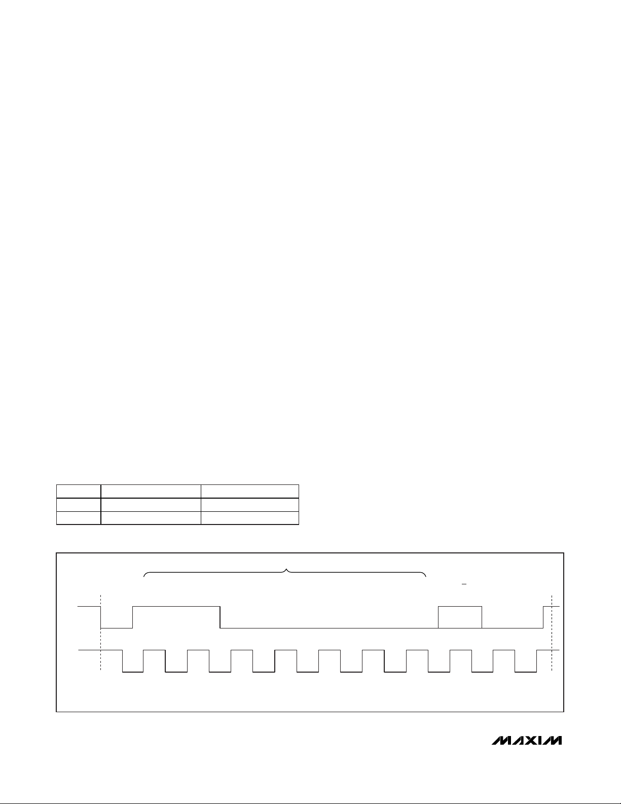
2-Wire Serial Interface
The MAX2165 uses a 2-wire I2C-compatible serial interface consisting of a serial-data line (SDA) and a serialclock line (SCL). SDA and SCL facilitate bidirectional
communication between the MAX2165 and the master
at clock frequencies up to 400kHz. The master initiates
a data transfer on the bus and generates the SCL signal to permit data transfer. The MAX2165 behaves as a
slave device that transfers and receives data to and
from the master. SDA and SCL must be pulled high
with external pullup resistors (1kΩ or larger) for proper
bus operation.
One bit is transferred during each SCL clock cycle. A
minimum of nine clock cycles is required to transfer a
byte in or out of the MAX2165 (8 bits and an ACK/NACK).
The data on SDA must remain stable during the high period of the SCL clock pulse. Changes in SDA while SCL is
high and stable are considered control signals (see the
START and STOP Conditions
section). Both SDA and
SCL remain high when the bus is not busy.
START and STOP Conditions
The master initiates a transmission with a START condition (S), which is a high-to-low transition on SDA while
SCL is high. The master terminates a transmission with
a STOP condition (P), which is a low-to-high transition
on SDA while SCL is high.
Acknowledge and Not-Acknowledge Conditions
Data transfers are framed with an acknowledge bit
(ACK) or a not-acknowledge bit (NACK). Both the master and the MAX2165 (slave) generate acknowledge
bits. To generate an acknowledge, the receiving device
must pull SDA low before the rising edge of the
acknowledge-related clock pulse (ninth pulse) and
keep it low during the high period of the clock pulse.
To generate a not-acknowledge condition, the receiver
allows SDA to be pulled high before the rising edge of
the acknowledge-related clock pulse, and leaves SDA
high during the high period of the clock pulse.
Monitoring the acknowledge bits allows for detection of
unsuccessful data transfers. An unsuccessful data
transfer happens if a receiving device is busy or if a
system fault has occurred. In the event of an unsuccessful data transfer, the bus master must reattempt
communication at a later time.
Slave Address
The MAX2165 has a 7-bit slave address that must be
sent to the device following a START condition to initiate communication. The slave address can be programmed to one of two possible addresses through the
ADDR pin (Table 20). The eighth bit (R/W) following the
7-bit address determines whether a read or write operation occurs.
The MAX2165 continuously awaits a START condition
followed by its slave address. When the device recognizes its slave address, it acknowledges by pulling the
SDA line low for one clock period; it is ready to accept
or send data depending on the R/W bit (Figure 1).
Write Cycle
When addressed with a write command, the MAX2165
allows the master to write to a single register or to multiple successive registers.
Table 20. Programmable Device Address
Figure 1. MAX2165 Slave Address Byte
I
2
C bus is a registered trademark of Philips Corp.
ADDR READ ADDRESS WRITE ADDRESS
1 0xC3 0xC2
0 0xC1 0xC0
SLAVE ADDRESS
S 1100000R/WACK
SDA
SCL
NOTE: TIMING PARAMETERS CONFORM WITH I
123456789
2
C BUS® SPECIFICATIONS.
P
Page 17
MAX2165
Single-Conversion DVB-H Tuner
______________________________________________________________________________________ 17
A write cycle begins with the bus master issuing a START
condition followed by the 7 slave address bits and a write
bit (R/W = 0). The MAX2165 issues an ACK if the slave
address byte is successfully received. The bus master
must then send to the slave the address of the first register it wishes to write to (see Table 1 for register addresses). If the slave acknowledges the address, the master
can then write one byte to the register at the specified
address. Data is written beginning with the most significant bit and is clocked in on the rising edge of SCLK. The
MAX2165 again issues an ACK if the data is successfully
written to the register. The master can continue to write
data to the successive internal registers with the
MAX2165 acknowledging each successful transfer, or it
can terminate transmission by issuing a STOP condition.
The write cycle does not terminate until the master issues
a STOP condition.
Figure 2 illustrates an example in which registers 0 through
2 are written with 0x0E, 0xD8, and 0xE1, respectively.
Read Cycle
All registers on the MAX2165 are available to be read by
the master with 3 of the registers being read-only.
A read cycle begins with the bus master issuing a
START condition followed by the 7 slave address bits
and a write bit (R/W = 0). The MAX2165 issues an ACK
if the slave address byte is successfully received. The
master then sends the address of the first register that it
wishes to read. The MAX2165 then issues another ACK.
Next, the master must issue a START condition followed
by the 7 slave address bits and a read bit (R/W = 1).
The MAX2165 issues an ACK if it successfully recognizes its address and begins sending data from the
specified register address starting with the most significant bit (MSB). Data is clocked out of the MAX2165 on
the rising edge of SCLK. On the 9th rising edge of
SCLK, the master can issue an ACK and continue reading successive registers, or it can issue a NACK followed by a STOP condition to terminate transmission.
The read cycle does not terminate until the master
issues a STOP condition. Figure 3 illustrates an example in which registers 0 and 1 are read back.
Applications Information
RF Input
The RF input is internally matched and provides good
return loss over the entire band of operation for either 50Ω
or 75Ω systems, and requires a DC-blocking capacitor.
RF and Baseband Gain Control
The MAX2165 features separate RF and baseband gaincontrol inputs that can be used to achieve optimum SNR
over a wide input dynamic range. Baseband gain control
is achieved through the BB_AGC pin. This pin is typically
controlled by the baseband processor and can accept
voltages from 0.4V to 2.3V with 2.3V providing maximum
baseband gain.
RF gain control is achieved through the RF_AGC pin. This
pin also accepts control voltages from 0.4V to 2.3V with
2.3V providing maximum RF gain. Closed-loop automatic
RF gain control can be achieved by connecting the
OVLD_DET pin through a lowpass filter to the RF_AGC
pin. See the
IF Power Detector
section.
The RF signal path features a low-noise amplifer (LNA)
that can be switched in an out-of-signal path. Program
the LNASW bit in the LNA register (Table 7) to 1 to enable
the LNA. Enabling the LNA adds about 17mA of current,
16dB of gain, and causes less than 10° of phase change
in the received signal.
IF Power Detector
The MAX2165 baseband power detector compares the
total weighted received input signal within approximately
2 channels of the wanted channel to a programmable
threshold. This threshold can be programmed to different values with the PD_TH[2:0] bits in the baseband
control register.
Figure 2. Example of Writing Registers 0 Through 2 with 0x0E, 0xDS, and 0xE1, Respectively
Figure 3. Example of Reading Data from Registers 0 Through 2
WRITE DEVICE
START
START START
ADDRESS
110000[ADDR] 0
WRITE DEVICE
ADDRESS
110000[ADDR] 0
R/W
R/W
ACK ACK
WRITE REGISTER
ACK ACK
ADDRESS
0x00
WRITE 1st REGISTER
ADDRESS
00000000
WRITE DATA TO
REGISTER 0x00
0x0E
WRITE DEVICE
ADDRESS
110000[ADDR]
ACK
R/W
1
WRITE DATA TO
REGISTER 0x01
0xD8
ACK
WRITE DATA
REG 0
D7–D0
WRITE DATA TO
ACK
REGISTER 0x02
0xE1
WRITE DATA
ACK
REG 1
D7–D0
ACK
STOP
NACK
STOP
Page 18

MAX2165
Single-Conversion DVB-H Tuner
18 ______________________________________________________________________________________
To close the RF gain-control loop, connect the 300µA
control current sink of the power detector (pin
OVLD_DET) to VCCwith a 40kΩ pullup resistor. The
resulting voltage is fed with an RC lowpass to the
RF_AGC input.
VCO Autotuner
The MAX2165 includes 3 VCOs with each VCO containing 8 VCO sub-bands. The appropriate VCO and VCO
sub-band for the desired local oscillator frequency can
be manually selected by programming the VCO[1:0]
and SB[2:0] bits in the VCO control register (Table 11).
Alternatively, the MAX2165 can be set to autonomously
choose a VCO and VCO sub-band. Automatic VCO
selection is enabled by setting the VAS bit in the VCO
Control register (Table 11). The autotuner begins
selecting the appropriate VCO once the fractional portion of the N-divider has been programmed. Therefore,
when changing LO frequencies, all the N-divider registers (integer and fractional) must be programmed to
activate the autotuner function.
PLL lock detection can be achieved by monitoring the
MUX pin or by reading the LD bit in the Chip-Status
Readback register (Table 18).
Charge-Pump Current Selection
The PLL charge-pump current can also be either manually programmed or automatically selected by the VCO
autotuner. Program the CPS bit in the PLL configuration
register (Table 8) to 1 to enable automatic charge-
pump-current selection, or program CPS to 0 to enable
manual charge-pump-current selection. The autotuner
function must be enabled (VAS = 1) to enable automatic charge-pump-current selection. When in manual
mode, the charge-pump current is programmed by the
ICP bit in the PLL Configuration register.
VCO Autotuner Delay Selection
During the autotuner selection process, the autotuner
must allow time for the PLL to settle before determining
if VCO selection was successful. This wait time is programmable through the ADLY[1:0] bits in the PLL
Configuration register (Table 8). Program the wait time
to be longer than the expected PLL settling time.
RF Notch Filter
The MAX2165 integrates an RF notch filter that can be
used to notch out large interfering signals in the
830MHz to 950MHz frequency range to prevent performance degradation when operating in the presence of
large cellular phone signals. The notch frequency of the
filter is programmable through the TF_NTCH[3:0] bits in
the Tracking Filter register (Table 6). Optimal notch filter codes for two different notch frequencies are stored
in an on-chip ROM table. See the
Baseband Filter and
Tracking Filter
section for additional details. When no
interfering cellular signals are present or when receiving
signals in the 783MHz to 860MHz frequency range, the
TF_NTCH[3:0] bits must be programmed to 111 to move
the notch out to the highest possible frequency to minimize the filter’s in-band attenuation.
Table 21. ROM Table
MSB LSB
DESCRIPTION ADDRESS
D7 D6 D5 D4 D3 D2 D1 D0
Reserved 0x0 X X X X X X X X
Optimal tracking
filter notch settings
for operation
below 725MHz
and above
725MHz
Optimal tracking
settings at
780MHz and
470MHz
Optimal baseband
filter BW for 8MHz
channel
0x1
0x2
0x3
TF_NTCH[3:0]
Tracking filter notch low
Recommended notch frequency settings for Rx
frequencies below 725MHz
TF_BAL[3:0]
Optimal tracking filter settings at 780MHz
BB_BW[3:0]
8MHz wide
DATA BYTE
TF_NTCH[3:0]
Tracking filter notch high
Recommended notch frequency settings for Rx
frequencies above 725MHz
TF_BAL[3:0]
Optimal tracking filter settings at 470MHz
XXXX
Page 19

MAX2165
Single-Conversion DVB-H Tuner
______________________________________________________________________________________ 19
Unlike the tracking filter, it is not necessary to interpolate
notch filter settings for various operating frequencies.
When receiving channels below 725MHz in the presence
of cellular blockers, the TF_NTCH[3:0] bits should be programmed to the lower notch frequency that is stored in
the ROM table. When receiving channels above 725MHz
in the presence of cellular blockers the TF_NTCH[3:0]
bits can be programmed to the upper notch frequency
that is stored in the ROM table.
Baseband Filter and Tracking Filter
The MAX2165 includes programmable baseband and
tracking filters. The baseband filter bandwidth is controlled through the BB_BW[3:0] bits in the Baseband
Control register (Table 12). The tracking filter’s balun frequency can be programmed through the TF_BAL[3:0] in
the Tracking Filter register (Table 6).
Reading the ROM Table
To accommodate process variations, each part is factory
calibrated. During calibration, the best notch filter settings
for two different notch frequencies, the best balun settings for 470MHz and 780MHz, and the best baseband
filter settings for 6MHz to 8MHz channels are determined.
These settings are stored in an on-chip ROM table that
must be read upon power-up and stored in the microprocessor local memory (3 bytes total). Table 21 shows
the address and bits for each ROM table entry.
Each ROM table entry must be read using a two-step
process. First, the address of the bits to be read must be
programmed into the TFA[3:0] bits in the ROM Table
Address register (Table 15).
Once the address has been programmed, the data
stored in that address is transferred to the TRF[7:0] bits in
the ROM Table Data Readback register (Table 17). The
ROM data at the specified address can then be read
from the TRF[7:0] bits and stored in the microprocessor’s
local memory.
Interpolating Balun Coefficients
The TF_BAL[3:0] bits must be reprogrammed for each
channel frequency to optimize performance over the
band. The values given for 780MHz and 470MHz in the
ROM table can be used to interpolate the optimal coefficients for any other frequency using the equation:
where:
Value = decimal value of the optimal TF_BAL[3:0] setting for desired channel frequency, f
BAL_L = decimal value of the optimal TF_BAL[3:0] setting for 470MHz as read from the ROM table
BAL_H = decimal value of the optimal TF_BAL[3:0] setting for 780MHz as read from the ROM table
f = desired channel frequency in MHz
Example: Assume the TF_BAL[3:0] values read from
the ROM table for 780MHz and 470MHz are 14 and 2,
respectively, and we wish to program the balun for
operation at an RF frequency of 620MHz.
Using the previous equation, we can calculate:
Rounding to the nearest integer value gives us 8; therefore, when operating at 620MHz, the TF_BAL[3:0] bits in
the Tracking Filter register must be programmed to 1000.
Setting the Baseband Filter
The MAX2165 baseband filter is freely programmable
over a wide range of 3dB cutoff frequencies from
approximately 3.0MHz to 4.3MHz, but the exact cutoff
frequency varies from part-to-part due to manufacturing process variations. To avoid requiring the user to
find the correct setting, the best setting for a 3.9MHz
cutoff frequency (i.e., 8MHz wide DVB-T/-H channels)
is determined by Maxim and stored on a ROM table on
every chip. The user needs to read this value from the
ROM table entry 0x3 (see Table 21) and write it back
into register 0xA bits BB_BW[3:0] (see Table 12) upon
powering up the MAX2165.
Baseband Filter Setting for RF Channels Other than
8MHz or Modulation Types Other than DVB-T
If a different cutoff frequency than 3.9MHz is desired, a
fixed value per Table 22 can be added or subtracted
from the number read-out of the ROM table, before
writing it back into the corresponding MAX2165 register.
This way the factory calibration is still utilized and the
resulting cutoff frequency is still reasonably accurate.
f 470MHz
Value BAL_L (BAL_H BAL_L) x
=+ −
−
780MHz 470MHz
−
Value at 620MHz 2 (14 - 2) x
=+
620MHz 470MHz
780MHz 470MHz
−
−
= 78.
Page 20
DC Offset Correction
Direct-conversion receivers are susceptible to DC offsets
that can limit linearity performance, as well as downstream data converter/demodulator dynamic range. The
MAX2165 includes on-chip fast-settling DC offset cancellation circuitry that requires no off-chip components to
remove any undesirable DC offsets that are present in the
output signal.
The correction threshold can be programmed to four different values through the DC_TH[1:0] bits in the DC
Offset Control register (Table 13).
When offset correction is active, the correction circuitry
creates a highpass characteristic in the signal path with
the highpass cutoff frequency determining the offset
correction speed. This correction speed is programmable through the DC_SP[1:0] bits in the DC Offset
Control register.
For DVB-H applications, it is recommended that the DC
correction be performed once after the part is taken out of
shutdown, then disabled by programming the
DC_SP[1:0] bits to 00 (hold state). Disabling the DC offset
correction during signal reception prevents the highpass
characteristic introduced by the correction circuitry from
distorting the lower frequency components of the
received signal and allows for DC-coupling to the demodulator. The only requirements for operation with DC-coupling are that the receive frequency and baseband filter
setting remain constant after the one-time cancellation.
The typical time-sliced operating nature of DVB-H easily
allows for operation under these conditions.
The part can be configured to automatically perform DC
correction upon power-up through the use of the SHDN
and STBY pins. See the
Power-Up Sequence
section for
further information.
Power-Up Sequence and Shutdown Modes
Driving the SHDN pin low places the MAX2165 in hardware shutdown mode, where all internal circuits are disabled and the supply current decreases to less than
20µA. Driving SHDN low shuts the entire IC down
regardless of the state of the internal registers except for
the shutdown reference bit (SHDN_REF). Register settings are maintained when the part comes out of shutdown mode.
The MAX2165 also features a software-shutdown mode.
In software-shutdown mode, the individual bits of the
Shutdown register can be programmed to power down
the MAX2165 functional blocks. Program the Shutdown
register (Table 10) to 0xFF, the VCO[1:0] bits in the VCO
Control register (Table 11) to 00, and the DC_MO[1:0]
bits in the DC Offset Control register (Table 13) to 00 to
shut down the entire chip through the software.
The MAX2165 features a power-up sequencer that very
quickly removes the DC offset upon exiting hardware
shutdown mode. To enable the power-up sequence feature, connect STBY to ground while SHDN transitions
from low to high.
Power-Up Sequence
Holding STBY low while SHDN transitions high causes the
part to power up in a two-step process. In the first step,
the VCO and PLL power up and settle. The typical current
consumption during this first step is approximately 20mA.
In the second step, the entire signal path is powered up
and the RF_AGC voltage, the BB_AGC voltage, and the
DC correction are automatically overridden with DC offset
correction performed in less than 0.5ms. Once DC correction has been achieved the part is returned to its originally programmed state. The entire power-up process
completes in approximately 2ms.
Table 22. Offsets for Various Cutoff Frequencies
MAX2165
Single-Conversion DVB-H Tuner
20 ______________________________________________________________________________________
DESIRED 3dB CUTOFF FREQUENCY (TYPICAL) (MHz)
3.10 -6
3.20 -5
3.30 -4
3.44 -3
3.56 -2
3.70 -1
3.90 0
4.10 +1
4.23 +2
OFFSET TO BE ADDED TO ROM TABLE ENTRY 0x3 BEFORE
WRITING BACK INTO REGISTER 0xA
Page 21

The benefit of the automatic DC correction is that it allows
the DC offset to be removed in less than 0.5ms, much
faster than the effective highpass corner frequency of the
correction circuit would otherwise allow. If the DC_SP[1:0]
bits are programmed to 00 prior to exiting hardware shutdown, the part performs a one-time DC offset cancellation
upon power up then disables the DC correction circuitry
after the power-up sequence completes. This allows for
DC-coupling between the baseband outputs and the
demodulator as long as the receive frequency, baseband
filter setting, and chip temperature stay constant after the
one-time cancellation. A change in these parameters
while the chip is receiving requires recalibration of the DC
offset. However, the typical time-sliced nature of DVB-H
does meet the above requirements for operation with
DC-coupling.
When STBY is connected to VCC, the chip does not follow
the power-up procedure described above, and all circuit
blocks are powered up at the same time. If the
DC_SP[1:0] bits are set to 00 (i.e., quasi-DC-coupled), a
DC calibration is never executed and the MAX2165 is not
functional.
The state of the STBY pin only determines whether or not
DC correction is automatically performed upon exiting
hardware shutdown.
Crystal-Oscillator Interface
The MAX2165 reference-oscillator input can be configured as a crystal oscillator or it can be used as a highimpedance reference input driven by an external source.
When using an external reference oscillator, drive XB
through an AC-coupling capacitor with a signal amplitude
of approximately 1V
P-P
and leave XE unconnected. The
phase noise of the external reference must exceed
-140dBc/Hz at offsets of 1kHz to 100kHz.
When connecting directly to a crystal, see the
Typical
Application Circuit
for the required topology.
Crystal-Oscillator Buffer Output
A buffered crystal-oscillator signal is provided at the
REFOUT pin and can be used to drive the demodulator.
This output requires a DC-blocking capacitor. This buffer
can be enabled or disabled through the SHDN_REF bit in
the Shutdown register (Table 10).
Layout Considerations
The EV kit can serve as a guide for PCB layout. Keep RF
signal lines as short as possible to minimize losses and
radiation. Use controlled impedance on all high-frequency traces. The exposed paddle must be soldered evenly
to the board’s ground plane for proper operation. Use
abundant vias beneath the exposed paddle for maximum
heat dissipation. Use abundant ground vias between RF
traces to minimize undesired coupling. To minimize coupling between different sections of the IC, the ideal
power-supply layout is a star configuration, which has a
large decoupling capacitor at the central VCCnode. The
VCCtraces branch out from this node with each trace
going to separate VCCpins of the MAX2165. Each V
CC
pin must have a bypass capacitor with a low impedance to ground at the frequency of interest. Do not
share ground vias among multiple connections to the
PCB ground plane.
MAX2165
Single-Conversion DVB-H Tuner
______________________________________________________________________________________ 21
Page 22
MAX2165
Single-Conversion DVB-H Tuner
22 ______________________________________________________________________________________
Typical Application Circuit
SERIAL-DATA
INPUT/OUTPUT
SERIAL-CLOCK
INPUT
ADDRESS
SELECT
CHARGE PUMP
MAX2165
V
CC
LDO
21
GND_TUNE
20
VTUNE
19
V
CC
VCC_VCO
18
17
16
15
BB_AGC
BBI+
BBI-
BASEBAND GAINCONTROL VOLTAGE
I+
I-
V
CC
BUFFERED
CRYSTAL
OUTPUT
V
CC
XE
+
SDA
1
SCL
2
3
N.C.
RFIN
4
ADDR
5
V
CC
VCC_RF
6
LEXT
7
XB
28
27 26 25
SERIAL INTERFACE, CONTROL,
AND SYNTHESIZER
EP
VCC_XTAL REFOUT MUX VCC_SYN CP
TO
CONTROL
BLOCK
DAC
+
LOCK
DETECT
24 23 22
0°
90°
PWRDET
-
8 9 10 11 12 13 14
SHDNRF_AGC
BBQ-
V
CC
BBQ+OLVD_DET VCC_BBSTBY
Q-
Q+SHUTDOWN STANDBY
Page 23
MAX2165
Single-Conversion DVB-H Tuner
______________________________________________________________________________________ 23
PACKAGE TYPE PACKAGE CODE DOCUMENT NO.
28 TQFN-EP T2855-8
21-0140
Package Information
For the latest package outline information and land patterns, go to www.maxim-ic.com/packages.
Page 24

MAX2165
Single-Conversion DVB-H Tuner
Maxim cannot assume responsibility for use of any circuitry other than circuitry entirely embodied in a Maxim product. No circuit patent licenses are
implied. Maxim reserves the right to change the circuitry and specifications without notice at any time.
24
____________________Maxim Integrated Products, 120 San Gabriel Drive, Sunnyvale, CA 94086 408-737-7600
© 2009 Maxim Integrated Products Maxim is a registered trademark of Maxim Integrated Products. Inc.
Revision History
REVISION
NUMBER
0 6/07 Initial release —
1 3/09
REVISION
DATE
DESCRIPTION
Added Note 3 to Spurious Emissions at RF Input specification, added condition to
Passband Cutoff Attenuation and Amplitude Ripple specifications, corrected Notes
1, 6, and 11
PAGES
CHANGED
3, 4, 5
 Loading...