

Page 1
General Description
The MAX2150 is a complete wideband direct upconversion quadrature modulator IC incorporating a 28-bit
sigma-delta fractional-N synthesizer. The device is targeted for applications in the 700MHz to 2300MHz frequency range.
The super-high-resolution sigma-delta fractional-N synthesizer is capable of better than 50mHz resolution
when used with a 10MHz reference. Other features:
fully differential I/Q modulation inputs, an internal LO
buffer, and a 50Ω wideband output driver amplifier.
A standard 3-wire interface is provided for synthesizer
programming and overall device configuration. An onchip low-noise crystal oscillator amplifier is also included and can be configured as a buffer when an external
reference oscillator is used.
The device typically achieves 34dBc of carrier and sideband suppression at a -1dBm output level. The wideband, internally matched RF output can also
be disabled while the synthesizer and 3-wire bus remain
powered up for continuous programming.
The device consumes 72mA from a single +3.0V supply and is packaged in an ultra-compact 28-pin QFN
package (5mm ✕5mm) with an exposed pad.
Applications
Wireless Broadband
Satellite Uplink
LMDS
Wireless Base Station
Features
♦ Single Voltage Supply (2.7V to 3.6V)
♦ 75MHz 3dB I/Q Input Bandwidth
♦ Wideband 50Ω RF Output: 700MHz to 2300MHz
♦ Ultra-Fine Frequency Resolution: 100mHz
♦ High Reference Frequency for Fast-Switching
Applications
♦ Ultra-Low Phase Noise
♦ Low Spurious and Reference Emissions
♦ -1dBm RMS Output Power
♦ 60dB RF Muting Control
♦ 34dBc Typical Carrier Suppression
♦ 34dBc Typical Sideband Suppression
♦ Software- and Hardware-Controlled Shutdown
Modes
MAX2150
Wideband I/Q Modulator with Sigma-Delta
Fractional-N Synthesizer
________________________________________________________________
Maxim Integrated Products
1
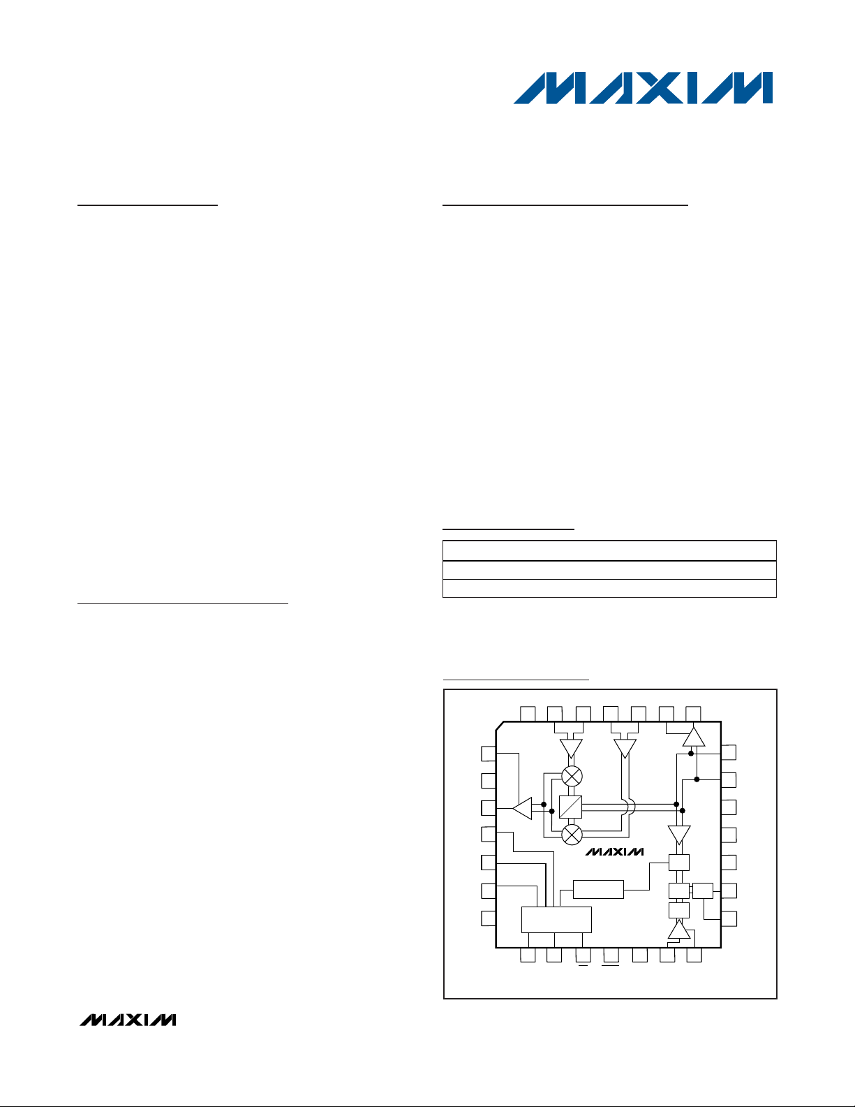
Pin Configuration/
Functional Diagram
Ordering Information
19-2389; Rev 4; 6/08
For pricing, delivery, and ordering information, please contact Maxim Direct at 1-888-629-4642,
or visit Maxim’s website at www.maxim-ic.com.
PART TEMP RANGE PIN-PACKAGE
MAX2150ETI -40°C to +85°C 28 TQFN-EP*
MAX2150ETI+ -40°C to +85°C 28 TQFN-EP*
*
EP = Exposed paddle.
+
Denotes lead-free package.
VCC_RF
I+ Q+I- Q- BUFOUTBUFEN
27
28
TXEN
1
VCC_PA
2
RFOUT
N.C.
N.C.
LOCK
VCC_SD
3
4
5
6
7
0
PROGRAMMING
AND CONTROL
9
8
CLK DATA SYNEN
26
90
∑ Δ – MOD
10
EN
25
MAX2150
11
SHDN
QFN
24
12
OSCIN VCC_XTAL
23
22
21
20
19
18
1/N
PFD
1/R
13
17
16
CHP
15
14
LO+
LO-
VCC_LO
VCC_D
VCC_A
CHP
VCC_CHP
Page 2
MAX2150
Wideband I/Q Modulator with Sigma-Delta
Fractional-N Synthesizer
2 _______________________________________________________________________________________
ABSOLUTE MAXIMUM RATINGS
Stresses beyond those listed under “Absolute Maximum Ratings” may cause permanent damage to the device. These are stress ratings only, and functional
operation of the device at these or any other conditions beyond those indicated in the operational sections of the specifications is not implied. Exposure to
absolute maximum rating conditions for extended periods may affect device reliability.
VCCto GND...........................................................-0.3V to +6.0V
RF Signals: LO+, LO-, OSCIN ........................................+10dBm
I+ to I-, Q+ to Q-.......................................................................2V
LO+, LO-, I+, I-, Q+, Q-, BUFEN, TXEN, CLK, DATA,
EN, SYNEN, OSCIN, OSCOUT, BUFOUT, CHP,
SHDN, LOCK, V
CC
_CP to GND..............-0.3V to (V
CC
+ 0.3V)
Digital Input Current .........................................................±10mA
Short-Circuit Duration RFOUT, BUFOUT, OSCOUT,
Lock, CHP...........................................................................10s
Continuous Power Dissipation
28-Pin TQFN (T
A
= +70°C)..................................................2W
(derate 28.5mW/°C above +70°C)
Operating Temperature Range ...........................-40°C to +85°C
Junction Temperature Range ..........................................+150°C
Storage Temperature.........................................-65°C to +150°C
Lead Temperature (soldering 10s) ..................................+300°C
DC ELECTRICAL CHARACTERISTICS
(MAX2150 EV kit. VCC= +2.7V to +3.6V, GND = 0V, SHDN = PLLEN = TXEN = high, BUFEN= low. No AC input signals. RFOUT and
BUFOUT output ports are terminated in 50Ω. T
A
= -40°C to +85°C. Typical values are at VCC= +3V, TA= +25°C, unless otherwise
noted.) (Note 1)
CAUTION! ESD SENSITIVE DEVICE
PARAMETER CONDITIONS MIN TYP MAX UNITS
SUPPLY
Supply Voltage 2.7 3 3.6 V
TX mode, SHDN = PLLEN = TXEN = high
BUFEN = low
72 107
Supply Current
LO Buffer Supply Current Additional current in all modes for BUFEN = high 3.3 5.5 mA
Shutdown Supply Current
CONTROL INPUT/OUTPUTS (SHDN, TXEN, SYNEN, BUFEN)
Input Logic High 2V
Input Logic Low 0.5 V
Input Logic High Current 1µA
Input Logic Low Current -1 µA
Lock Detect High (Locked) 2 V
Lock D etect Low ( U nl ocked ) 0.5 V
Power-Up Time MOD mode 25 µs
Power-Down Time MOD mode 1 µs
3-WIRE CONTROL INPUT (CLK, DATA, EN)
Input Logic High
Input Logic Low 0.5 V
Input Logic High Current 1µA
Input Logic Low Current -1 µA
SYNTH mode, SHDN = PLLEN = high, TXEN =
BUFEN = low
MOD mode, SHDN = TXEN = high, SYNEN =
BUFEN = low
HW_SHDN mode, SHDN = low 0.3 600
SW_SHDN mode, PWDN bit at logic low 35 600
V
CC
0.5
25 38
46 69
-
mA
µA
V
Page 3
MAX2150
Wideband I/Q Modulator with Sigma-Delta
Fractional-N Synthesizer
_______________________________________________________________________________________ 3
AC ELECTRICAL CHARACTERISTICS
(MAX2150 EV kit. VCC= +2.7V to +3.6V, SHDN = PLLEN = TXEN = high, BUFEN =low. Input I/Q signals: F
I/Q
= 500kHz, V
I/Q
= 1V
P-P
.
I+, Q+ single-ended input, driven from AC-coupled source. I-, Q- single-ended inputs are AC-coupled to GND. RFOUT and BUFOUT
output ports are terminated in 50Ω loads. f
LO
=1750MHz, PLO= -10dBm, typical values are at VCC= +3V, TA= +25°C, unless other-
wise noted.) (Note 1)
MODULATION INPUT
I/Q Input Bandwidth
I/Q Differential Input Level
I/Q DC Input Resistance 200 kΩ
I/Q Common-Mode Input Range (Note 2) 1.5 1.6 1.7 V
RF OUTPUT
Frequency Range 700 2300 MHz
Output Power
Output 1dB Compression Point 1 dBm
Output IP3 14 dBm
Carrier Suppression fRF = 1750MHz 34 dBc
Sideband Suppression fLO - f
RF Output Noise Floor f
Output Return Loss (Note 3) -9 dB
LO INPUT/OUTPUT
Frequency Range 700 2300 MHz
LO Input Power (Note 2) -12 -10 -7 dBm
LO Input Return Loss fLO =2000MHz -15 dB
LO Buffer Output Level BUFEN = high (Note 2) -14 -9.5 dBm
SIGMA-DELTA FRACTIONAL-N SYNTHESIZER
SYSTEM REQUIREMENTS
Frequency Range
Phase-Detector Input-Referred
Phase Noise Floor
In-Loop Spurious Emissions
MAIN DIVIDER AND PHASE DETECTOR
Minimum Fractional-N Step Size
Phase-Detector Comparison
Frequency
Maximum N Division 251
Minimum N Division 35
PARAMETER CONDITIONS MIN TYP MAX UNITS
BW (-1dB) 26
BW (-3dB) 75
Assumes a sine-wave input to achieve the RFOUT output
power specified below
TXEN = high, fRF = 1750MHz -7 -1
TXEN = low, f
(Note 2)
f
f
= CPX = 1 (Note 5)
= 1750MHz -60
RF
, fRF = 1750MHz 25 34 dBc
I/Q
> 40MHz (Note 2) -148 -143 dBm/Hz
OFFSET
700 2300 MHz
= f
COMP
= 1740.005MHz, f
LO
= 20MHz, CP0 = CP1 = CPX = 1 (Note 4) -138 dBc/Hz
REF
= f
COMP
= 20MHz, CP0 = CP1
REF
1V
-40 dBc
f
/
COMP
28
2
20 30 MHz
MHz
dBm
P-P
Page 4
MAX2150
Wideband I/Q Modulator with Sigma-Delta
Fractional-N Synthesizer
4 _______________________________________________________________________________________
AC ELECTRICAL CHARACTERISTICS (continued)
(MAX2150 EV kit. VCC= +2.7V to +3.6V, SHDN = PLLEN = TXEN = high, BUFEN = low. Input I/Q signals: F
I/Q
= 500kHz, V
I/Q
= 1V
P-P
.
I+, Q+ single-ended input, driven from AC-coupled source. I-, Q- single-ended inputs are AC-coupled to GND. RFOUT and BUFOUT
output ports are terminated in 50Ω loads. f
LO
=1750MHz, PLO= -10dBm, typical values are at VCC= +3V, TA= +25°C, unless other-
wise noted.) (Note 1)
Note 1: Parameters are guaranteed by production testing at +25°C and +85°C. Minimum and maximum values over the tempera-
ture and supply voltage range are guaranteed by design and characterization.
Note 2: Guaranteed by design and characterization.
Note 3: Measured with MAX2150 EV kit.
Note 4: Measured with an on-chip crystal oscillator.
Note 5: In-loop spurious emissions occur when synthesizing a frequency at an integer multiple of the comparison frequency with
fractional offset within the PLL loop BW.
Note 6: If an on-chip oscillator is used, a fundamental tone crystal is needed.
Note 7: Minimum and maximum values at CPX = 1 are guaranteed by production testing. Values at CPX = 0 are guaranteed by
design and characterization.
REFERENCE OSCILLATOR AND DIVIDER
Input Frequency Range 10 50 MHz
AC-Coupled Input Sensitivity AC-coupled, single ended (Note 2) 0.4 2.3 V
Reference Division Ratio (Notes 2, 6) 1 4
CHARGE-PUMP OUTPUT
Charge-Pump Current (Note 7)
Charge-Pump Voltage
Compliance
PARAMETER CONDITIONS MIN TYP MAX UNITS
CP1, CP0 = 00
CP1, CP0 = 01
CP1, CP0 = 10
CP1, CP0 = 11
Sink/source currents match within ±5% 0.5
CPX = 0 0.12 0.17 0.22
CPX = 1 0.23 0.34 0.44
CPX = 0 0.23 0.35 0.46
CPX = 1 0.47 0.67 0.88
CPX = 0 0.36 0.52 0.68
CPX = 1 0.70 1.00 1.30
CPX = 0 0.48 0.69 0.90
CPX = 1 0.91 1.31 1.70
VCC -
0.5
P-P
mA
V
Page 5
MAX2150
Wideband I/Q Modulator with Sigma-Delta
Fractional-N Synthesizer
_______________________________________________________________________________________
5
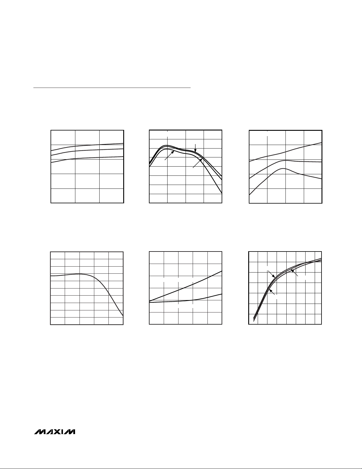
Typical Operating Characteristics
(MAX2150 EV kit. VCC= +3V, SHDN = PLLEN = TXEN = high, BUFEN = low. Input I/Q signals: F
I/Q
= 500kHz, V
I/Q
= 1V
P-P
. I+, Q+ single-ended input, driven from AC-coupled source. I-, Q- single-ended inputs are AC-coupled to GND. RFOUT and BUFOUT output ports
are terminated in 50Ω loads. f
LO
=1750MHz, PLO= -10dBm, TA= +25°C, unless otherwise noted.)
SUPPLY CURRENT
vs. SUPPLY VOLTAGE
100
TX MODE
80
60
40
SUPPLY CURRENT (mA)
20
0
2.7 3.6
+85°C
+25°C
-40°C
SUPPLY VOLTAGE (V)
MODULATION OUTPUT POWER
vs. FREQUENCY
4
TXEN = HIGH
2
MAX2150 toc01
0
-2
+85°C
-4
-6
-8
MODULATION OUTPUT POWER (dBm)
-10
-12
3.33.0
700 2300
-40°C
+25°C
FREQUENCY (MHz)
MAX2150 toc02
190015001100
CARRIER AND SIDEBAND
OUTPUT POWER vs. LO POWER
-1.0
-1.1
-1.2
-1.3
-1.4
-1.5
-1.6
OUTPUT POWER (dBm)
-1.7
-1.8
-1.9
-2.0
712
LO POWER (dBm)
11108 9
MAX2150 toc04
CARRIER AND SIDEBAND SUPPRESSIONS (dB)
SUPPRESSIONS vs. LO POWER
38
37
36
SIDEBAND SUPPRESSION
35
34
CARRIER SUPPRESSION
33
32
712
LO POWER (dBm)
111098
MAX2150 toc05
MODULATION OUTPUT POWER
vs. FREQUENCY
-55
TXEN = LOW
-58
-61
-64
-67
MODULATION OUTPUT POWER (dBm)
-70
700 2300
-40°C
+25°C
+85°C
FREQUENCY (MHz)
MODULATOR OUTPUT POWER
vs. I/Q INPUT LEVEL
4
0
-4
-8
-12
-16
MODULATOR OUTPUT POWER (dBm)
-20
-24
-40°C
+25°C
+85°C
0
I/Q INPUT LEVEL (mV)
190015001100
140012001000800600400200
MAX2150 toc03
MAX2150 toc06
Page 6

MAX2150
Wideband I/Q Modulator with Sigma-Delta
Fractional-N Synthesizer
6 _______________________________________________________________________________________
Typical Operating Characteristics (continued)
(MAX2150 EV kit. VCC= +3V, SHDN = PLLEN = TXEN = high, BUFEN = low. Input I/Q signals: F
I/Q
= 500kHz, V
I/Q
= 1V
P-P
. I+, Q+
single-ended input, driven from AC-coupled source. I-, Q- single-ended inputs are AC-coupled to GND. RFOUT and BUFOUT output
ports are terminated in 50Ω loads. f
LO
=1750MHz, PLO= -10dBm, TA= +25°C, unless otherwise noted.)
MODULATOR OUTPUT IP3 vs. V
16
15
14
13
12
MODULATOR OUTPUT IP3 (dBm)
11
10
2.7 3.6
+85°C
+25°C
-40°C
VCC (V)
3.33.0
CC
MAX2150 toc07
MODULATOR OUTPUT P1dB vs. V
3.0
2.5
2.0
1.5
1.0
0.5
0
MODULATOR OUTPUT P1dB (dBm)
-0.5
-1.0
2.7 3.6
+85°C
+25°C
-40°C
3.33.0
VCC (V)
CC
MAX2150 toc08
LO PORT RETURN LOSS (dB)
-10
-15
-20
-25
-30
LO PORT INPUT RETURN LOSS
vs. FREQUENCY
0
-5
700 2300
FREQUENCY (MHz)
190015001100
MAX2150 toc09
BUFOUT PORT RETURN LOSS
vs. FREQUENCY
0
-5
-10
-15
-20
BUFOUT PORT RETURN LOSS (dB)
-25
-30
700 2300
FREQUENCY (MHz)
190015001100
-4
-5
MAX2150 toc10
-6
-7
-8
-9
-10
-11
-12
LO BUFFER OUTPUT POWER (dBm)
-13
-14
700 2300
LO BUFFER OUTPUT POWER
vs. FREQUENCY
BUFEN = HIGH
+85°C
+25°C
-40°C
FREQUENCY (MHz)
LO BUFFER OUTPUT POWER
vs. FREQUENCY
-40
BUFEN = LOW
MAX2150 toc11
-43
-46
-49
-52
LO BUFFER OUTPUT POWER (dBm)
-55
190015001100
700 2300
+85°C
FREQUENCY (MHz)
+25°C
-40°C
190015001100
MAX2150 toc12
Page 7

MAX2150
Wideband I/Q Modulator with Sigma-Delta
Fractional-N Synthesizer
_______________________________________________________________________________________
7
Typical Operating Characteristics (continued)
(MAX2150 EV kit. VCC= +3V, SHDN = PLLEN = TXEN = high, BUFEN = low. Input I/Q signals: F
I/Q
= 500kHz, V
I/Q
= 1V
P-P
. I+, Q+
single-ended input, driven from AC-coupled source. I-, Q- single-ended inputs are AC-coupled to GND. RFOUT and BUFOUT output
ports are terminated in 50Ω loads. f
LO
=1750MHz, PLO= -10dBm, TA= +25°C, unless otherwise noted.)
OSCIN PORT SENSITIVITY
(SYNTHESIZER) vs. FREQUENCY
6
5
4
3
+25°C
2
OSCIN PORT SENSITIVITY (V)
1
-40°C
0
10 50
-40°C
+25°C
+85°C
+85°C
FREQUENCY (MHz)
SYNTHESIZER PHASE NOISE
0
-10
-20
-30
-40
-50
-60
-70
-80
-90
-100
-8.5dBm
N/C = -99dBc/Hz
SPAN = 20kHzCENTER = 1.75MHz
MAX2150 toc13
45403530252015
0.60
0.50
0.40
0.30
0.20
0.10
0
MAX2150 toc15
OSCIN IMPEDANCE vs. FREQUENCY
0
-100
-200
-300
-400
-500
-600
-700
OSCIN PORT IMPEDANCE (Ω)
-800
-900
-1000
REAL
IMAGINARY
10 50
FREQUENCY (MHz)
I/Q MODULATOR OUTPUT SPURS
-10
-20
-30
-40
-50
-60
-70
-80
-90
-100
0
1 AVG
CARRIER
SUPPRESSION
-34dBc
454030 3520 2515
MAX2150 toc16
SIDEBAND
SUPPRESSION
-36dBc
SPAN = 2 MHzCENTER = 1.75 GHz
MAX2150 toc14
Page 8

MAX2150
Wideband I/Q Modulator with Sigma-Delta
Fractional-N Synthesizer
8 _______________________________________________________________________________________
Pin Description
PIN NAME FUNCTION
1 TXEN
2 VCC_PA
3 RFOUT
4, 5 N.C. Do Not Connect. (These pins must be left floating.)
6 LOCK Lock Status of the PLL. A static logic-level high indicates that the PLL is in the locked condition.
7 VCC_SD
8, 9, 10
11 SHDN
12 SYNEN
13 OSCIN
CLK, DATA,ENInput Pins from 3-Wire Serial Bus. An RC lowpass filter on each of these pins can be used to reduce
Modulator Enable Input. Set TXEN low to inhibit the RF and modulator circuits. This mode can be used
for quiet frequency synthesis.
Supply Voltage Input for RFOUT Output Driver Circuits. Bypass as close to the pin as possible. The
bypass capacitor should not share ground vias with other branches.
Modulator RF Output. This is a wideband, internally matched 50Ω output. A DC-blocking capacitor is
required.
Supply Voltage Input for Sigma-Delta Modulator Circuits. Bypass as close to the pin as possible. The
bypass capacitor should not share ground vias with other branches.
digital noise.
Shutdown Control. Set SHDN low to disable all internal circuits for lowest power consumption. An RC
lowpass filter can be used to reduce digital noise.
Synthesizer Enable Input. Set SYNTH low to disable the internal frequency synthesizer. An RC lowpass
filter can be used to reduce digital noise.
Reference Oscillator Input. Connect a parallel, resonant, fundamental-tone crystal between this pin and
ground to facilitate a crystal oscillator circuit. For applications with an external reference oscillator, the
OSCIN input can be driven through a large-value series capacitor.
14 VCC_XTAL
15 VCC_CHP
16 CHP
17 VCC_A
18 VCC_D
19 VCC_LO
20, 21 LO-, LO+
22 BUFOUT Buffered LO Output. Internally matched to 50Ω, requires a DC-blocking capacitor.
23 BUFEN
24, 25 Q-, Q+
Supply Voltage Input for Crystal Oscillator. Bypass as close to the pin as possible. The bypass capacitor
should not share ground vias with other branches.
Supply Voltage Input for Charge Pump. Bypass as close to the pin as possible. The bypass capacitor
should not share ground vias with other branches.
High-Impedance Charge-Pump Output. Connect to the tune input of the VCO through the PLL loop filter.
Keep the line from this pin to the tune input as short as possible to prevent spurious pickup, and
connect the loop filter as close to the tune input as possible.
Supply Voltage Input for PLL. Bypass as close to the pin as possible. The bypass capacitor should not
share ground vias with other branches.
Supply Voltage Input for PLL. Bypass as close to the pin as possible. The bypass capacitor should not
share ground vias with other branches.
Supply Voltage Input for Internal LO Circuits. Bypass as close to the pin as possible. The bypass
capacitor should not share ground vias with other branches.
Differential Local-Oscillator Input. These inputs require DC-blocking capacitors. The LO can be applied
with a single-ended input to the LO+/LO- pin. In this mode, the other pin should be AC-grounded.
LO Output Buffer Amplifier Enable. Set BUFEN high to enable the on-chip output LO buffer for driving
external circuits. An RC lowpass filter can be used to reduce digital noise.
Differential Q-Channel Baseband Inputs to the Modulator. These pins connect directly to the bases of
a differential pair and require an external common-mode bias voltage of 1.6V.
Page 9

Detailed Description
Internally, the MAX2150 includes a broadband I/Q
modulator, internally matched broadband output driver
amplifier, fine-resolution fractional-N frequency synthesizer, an LO buffer amplifier, and an on-chip low-noise
crystal oscillator circuit.
A simple 3-wire interface is provided for synthesizer
programming and device configuration and control.
Independent hardware and software power-down control of the I/Q modulator, frequency synthesizer, and LO
buffer amplifier is provided, as well as the ability to shut
down the entire chip.
I/Q Modulator
The MAX2150 modulator is composed of a pair of
matched double-balanced mixers, a broadband passive LO quadrature generator, and a summing amplifier. The mixers accept differential I/Q baseband signals
that directly modulate the internal 0° and 90° LO signals applied to the I/Q mixers. An external LO source
drives an internal LO quadrature generator that shifts
the phase of the LO signal applied to the Q mixer by
90° relative to the LO signal applied to the I-channel
mixer. The modulated output of the I/Q mixers is
summed together, and the undesired sideband is suppressed.
The I+, I-, Q+, and Q- input ports feature high-linearity
buffer amplifiers with a typical -3dB bandwidth of
75MHz and accept differential input voltages up to
1V
P-P
. The ports require external biasing and have an
input common-mode requirement of 1.6V. For singleended operation, bypass the I and Q ports to ground.
See the
Typical Application Circuit
for recommended
component values.
The broadband output driver amplifier is matched on
chip across the entire operating frequency range and
requires an output DC-blocking capacitor. For optimum
performance, the output match can be improved with
simple L-section and/or PI-section matching networks.
Always ensure that DC blocking is provided, because
internal bias voltages are present at this output.
The modulator can be shut down with both hardware
(pin 1) and software (TE bit). This mode is useful for
quiet synthesizer programming or to mute the RF output signal. The hardware pin and software bits must be
set to logic-1 to enable the modulator. If the hardware
pin or software bit is set to logic-0, or if both are set to
logic-0, the modulator is disabled.
LO Buffer Amplifier
The broadband buffer amplifier output is internally
matched and requires a DC-blocking capacitor to isolate on-chip bias voltages. Power-down of the LO buffer
can be controlled by both BUFEN (pin 23), as well as
BUFEN by software by setting the BUFEN (BE) bit
through the 3-wire interface. The hardware pin and the
software bit must be a logic-1 to enable the buffer. If
the hardware or software bit is set to logic-0, the LO
buffer is disabled.
Frequency Synthesizer
The MAX2150 features an internal 28-bit sigma-delta
frequency synthesizer. This architecture enables the
use of very high (30MHz) comparison frequencies,
which significantly reduces the in-loop phase noise as
a result of reduced division ratios. The high comparison
frequency also allows significantly increased PLL
bandwidths for very fast switching speed applications.
Divider Programming
The MAX2150 frequency programming is determined
as follows. The overall division ratio (D) has an integer
value (N), as well as a fractional component (F):
D = N.F = N +F / 2
28
The N and F values are encoded as straight binary
numbers. Determination of these values is illustrated by
the following example:
F
LO
= 1721.125MHz, F
COMP
= 20MHz
Then:
D = 1721.125 / 20 = 86.05625
Therefore:
N = 86 and F = 0.05625 x 228= 15,099,494
MAX2150
Wideband I/Q Modulator with Sigma-Delta
Fractional-N Synthesizer
_______________________________________________________________________________________ 9
Pin Description (continued)
PIN NAME FUNCTION
26, 27 I-, I+
28 VCC_RF
— Exposed pad Ground
Differential I-Channel Baseband Inputs to the Modulator. These pins connect directly to the bases of a
differential pair and require an external common-mode bias voltage of 1.6V.
Supply Voltage Input for RF Circuits. Bypass as close to pin as possible. The bypass capacitor should
not share ground vias with other branches.
Page 10

MAX2150
Converting each to binary representation results in the
following:
N register = 86 = 0101,0110
F register value =
0000,1110,0110,0110,0110,0110,0110
The F-register value is then split between an upper 14
bits and a lower 14 bits as follows:
Upper 14 bits + address 00 = 0000,1110,0110,0100
Lower 14 bits + address 01 = 1001,1001,1001,1001
Synthesizer Shutdown
The synthesizer can be disabled by setting SYNEN (pin
12) to a logic low. This mode is useful when an external
frequency synthesizer is employed.
Applications Information
Serial Interface and Register Definition
3-Wire Interface and Registers
The MAX2150 is programmed through a simple
3-wire (CLK, DATA, EN) interface. The programming
data is contained within 16-bit words loaded into four
unique address locations. Each location contains programming information for setting operational modes
and device configuration. Two words (address 00, 01)
control the fractional divide number in the sigma-delta
synthesizer. The third word (address 10) sets the integer divide value, reference divide value, charge-pump
current, and charge-pump compensation DAC settings.
The fourth and final word (address 11) contains various
device configuration registers and test registers, as
well as additional charge-pump compensation registers. See Tables 1 through 11 for details.
3-Wire Interface Timing Diagram
Figure 1 shows the programming logic. The 16-bit shift
register is programmed by clocking in data at the rising
edge of CLK. Pulling enable low allows data to be
clocked into the shift register; pulling enable high loads
the register addressed.
Fractional Spurs
When synthesizing a frequency that is an integer multiple of the reference divider and having a fractional offset with a value less than the PLL filter bandwidth,
fractional spurs can be observed at a typical level of
-40dBc. For example, to synthesize 1640.005MHz
when using a 20MHz reference and a PLL bandwidth of
25kHz, spurious products offset from the LO by 5kHz
can be observed. The 1640MHz is an integer multiple
of 20MHz, and the fractional offset of 5kHz is within the
PLL bandwidth.
It is possible to avoid the above-mentioned spurious
products by using two reference oscillators with slightly
offset frequencies or by using a higher reference frequency and changing the comparison frequency of the
reference divider.
Crystal Oscillator
The MAX2150 includes a simple-to-use on-chip lownoise reference oscillator circuit. The oscillator is
formed by connecting a fundamental mode parallel resonant crystal from OSCIN to ground. The oscillator circuit is useful from 10MHz to 50MHz.
The phase noise of the MAX2150 can be improved by
using a precision high-frequency external reference
oscillator (TCXO). The external oscillator is connected
through a DC-blocking capacitor directly to the OSCIN
pin.
Layout Considerations
A properly designed PC board is an essential part of
any RF circuit. A ground plane is essential. Keep RF
signal lines as short as possible to reduce losses, radiation, and inductance. The exposed pad on the underside of the MAX2150 must be adequately grounded by
ensuring that the exposed paddle of the device package is soldered evenly to the board ground plane. Use
multiple, low-inductance vias to ground the exposed
paddle.
Wideband I/Q Modulator with Sigma-Delta
Fractional-N Synthesizer
10 ______________________________________________________________________________________
Figure 1. 3-Wire Interface Timing Diagram
B19 (MSB) B18 B0 A3 A1 A0 (LSB)
DATA
CLK
t
CS
EN
t
CH
t
CWL
t
CWH
t
ES
t
EW
tCS > 50ns
t
> 10ns
CH
t
> 50ns
CWH
t
> 50ns
ES
t
> 50ns
CWL
t
> 50ns
EW
Page 11

MAX2150
Wideband I/Q Modulator with Sigma-Delta
Fractional-N Synthesizer
______________________________________________________________________________________ 11
Table 2. Reference Divider
Table 3. Integer Divider-N*
Table 4. Fractional Divider-F (Upper 14 Bits)
Table 5. Fractional Divider-F (Lower 14 Bits)
*N divider is limited to 35 < N < 251.
Table 1. Register Tables
MSB SHIFT REGISTER DATA LSB ADDRESS
Upper (MSBs) Fractional Divider Value (F) 14 Bits (Default = 8192, 10000000000000) Address
27 26 25 24 23 22 21 20 19 18 17 16 15 14 0 0
Lower (LSBs) Fractional Divider Value (F)14 Bits (Default 0 DEC, 00000000000000 Address
13 12 11 10 9 8 7 6 5 4 3 2 1 0 0 1
R Divider
Default = 00
R1 R0 LIN1 LIN0 CP1 CP0 7 6 5 4 3 2 1 0 1 0
Reset Delay
Default = 00
BL1 BL0 T5 T4 T3 T2 T1 T0 INT PD TE BE XX CPX 1 1
R1 R0 REFERENCE DIVIDE VALUE
00 1
01 2
10 3
11 4
N7 N6 N5 N4 N3 N2 N1 N0 INTEGER DIVIDE VALUE
0 0100011 35
0 0100100 36
— ——————— —
1 1111010 250
1 1111011 251
CP Bleed
Default = 00
CP Current
Default = 11
Test Registers 6 Bits
Default = 0 DEC
Integer Divide Value (N) 8 Bits
Default = 177 DEC
Control Register 6 Bits
Default = 15 DEC
Address
Address
F27 F26 F25 F24 F23 F22 F21 F20 F19 F18 F17 F16 F15 F14
00000000000000
00000000000000
——————————————
11111111111111
F13 F12 F11 F10 F9 F8 F7 F6 F5 F4 F3 F2 F1 F0
00000000000000 1
00000000000001 2
—————————————— —
11111111111110 268435454
11111111111111 268435455
INTEGER DIVIDE
VALUE
Page 12

MAX2150
Power-Supply (VCC) Bypassing
Proper voltage-supply bypassing is essential to reduce
the spurious emissions mentioned above. It is recommended that each VCCpin be bypassed independently
and share no common vias with any other ground connection. See the
Typical Operating Circuit
for suggest-
ed bypass component values.
Wideband I/Q Modulator with Sigma-Delta
Fractional-N Synthesizer
12 ______________________________________________________________________________________
Table 6. Control Register
Table 7. Device Modes
BIT ID
CPX CP_MULT 1 0
XX XX XX 1 Unused.
BE BUFEN 1 2 High enables the VCO buffer. Low disables this output.
TE TXEN 1 3
PD PWDN 0 4
INT INT_MODE 0 5
BIT
NAME
PWR-UP
STATE
BIT LOCATION
0 = LSB
FUNCTION
A logic high doubles the charge pump current selected through registers
CP1 and CP0. Logic low sets the charge-pump current to the value
selected by registers CP1 and CP0.
Low enables SW_MUTE mode, which shuts down the RF circuits while
leaving the 3-wire interface, register, and PLL circuits active.
Low enables register-based shutdown. This mode shuts down all circuits
except the 3-wire interface and internal registers.
Logic high disables the sigma-delta modulator. Logic low enables the
sigma-delta modulator for normal operation.
MODE
SHDN TXEN SYNEN BUFEN PWDN TXEN BUFEN
TX H H H H/L H H H/L All circuits active.
MOD H H L H/L H H H/L
SYNTH H L H H/L H X H/L
SW_MUTE H H H H/L H L H/L
HW_SHDN L X X X X X X
SW_SHDN H X X X L X X
HW PINS
SOFTWARE CONTROL
BITS
Modulator circuits active. Synthesizer
blocks disabled. Mode is used with external
PLL circuit.
Serial interface and synthesizer blocks
active. RF and modulator blocks disabled.
Mode is used to gate RF ON/OFF with
external logic control.
Serial interface and synthesizer blocks all
active. Modulator blocks disabled. Mode is
used to gate RF ON/OFF with software
control.
All circuits disabled. Lowest current mode
of operation.
Serial interface and registers active, all
other circuits inactive regardless of the
state of the HW pins with the exception of
HW_SHDN.
DESCRIPTION
Page 13

MAX2150
Wideband I/Q Modulator with Sigma-Delta
Fractional-N Synthesizer
______________________________________________________________________________________ 13
Table 8. TXEN Pin and Software Bit
Definitions
Table 11. BUFEN Pin and Software Bit
Definitions
Table 9. Charge-Pump Registers
Table 10. Test Register Definition
(Default 0 Dec)*
*
All other logic states are undefined.
Chip Information
TRANSISTOR COUNT: 16,321
Package Information
For the latest package outline information and land patterns, go
to www.maxim-ic.com/packages
.
PACKAGE TYPE PACKAGE CODE DOCUMENT NO.
28 TQFN-EP T2855-3
21-0140
TXEN
PIN BIT
0 0 TX off
0 1 TX off
1 0 TX off
1 1 TX enabled
TX MODE
CPX CP1 CP0 ICP (µA)
0 0 0 170
0 0 1 350
0 1 0 520
0 1 1 690
1 0 0 340
1 0 1 670
1 1 0 1000
1 1 1 1310
BUFEN
PIN BIT
0 0 Buffer off
0 1 Buffer off
1 0 Buffer off
1 1 Buffer on
BUF MODE
TEST MODE T5 T4 T3 T2 T1 T0 TEST PIN
Normal
Operating
Mode
Charge Pump
Forced to
Source Icp
Charge Pump
Forced to Sink
Icp
Reference
Divider Output
Main Divider
Output
000000 —
000001 CP
000010 CP
0 1 0 0 0 0 Lock
0 1 1 0 0 0 Lock
Page 14

MAX2150
Wideband I/Q Modulator with Sigma-Delta
Fractional-N Synthesizer
14 ______________________________________________________________________________________
Typical Operating Circuit
J6
VCC
J7
GND
J8
RFOUT
VCC
LOCK
DCIN
VCC
C25
1μF
R13
0Ω
C15
OPEN
J20
VCCSD
C31
0.1μF
C27
1.0μF
C16
OPEN
C17
100pF
0.1μF
J1
31-5239-52RFX
IIN QNQ
C50
0.1μF
R31
R29
OPEN
C28
0.1μF
VCC
C14
100pF
0.1μF
C3
1
TXEN
2
V
CC
3
RFOUT
4
TEST2
5
TEST1
6
LOCK
7
V
CC
3.3kΩ
R32
3.3kΩ
R33
3.3kΩ
R34
3.3kΩ
VCC
VCC_RF28I+
_PA
_SD
CLK8DATA
JUMP_PAD
VCC
C18
J16
J17
R1
OPEN
C2
100pF
27
26
I-
EN
9
0.1μF
C37
OPEN
10
VCC
L1
EN
OPEN
R2
J2
31-5239-52RFX
C52
0.1μF
R3
OPEN
25
Q+
U1
MAX2150
SHDN
SYNEN12OSCIN VCC_XTAL
11
SHDN
R4
OPEN
C1
0.1μF
13 14
22
V
V
CC
Q-24BUFEN23BUFOUT
CC
V
CC
VCC_A
_CHP
CHP
LO+
LO-
_LO
_D
C13
100pF
BUFEN
21
20
19
18
17
16
15
VCC
R12
0Ω
C5
OPEN
C7
OPEN
C8
22pF
C12
VCC
100pF
C4
VCC
100pF
C11
100pF
C22
6800pF
C10
100pF
VCC
C9
VCC
100pF
C19
0.1μF
VCC
C21
0.1μF
C20
0.1μF
R23
245Ω
C32
0.1μF
1.1kΩ
C23
.068μF
R24
C6
OPEN
J15
1
2
3
VCC_VCO
LOn
VT
GND
VCC
0.1μF
C35
100pF
C24
680pF
C33
R25
1.1kΩ
J13
BUFOUT
J14
LO
VC3R0A230967/
U2
1750B350FUJI
7
6
GND
VSW
5
GND
4
OUT
GND
8
J19
J5
R35
OPEN
VCCVCO
J11
GND
TUNEOUT
C34
0.1μF
C26
470pF
VTUNE_OUT
C30
0.1μF
R18
0Ω
Y1
REFL In
J18
J10–1
J10–2
LOCK
J10–3
J10–4
C36
0.1μF
FILTVCC
J10–11
J10–12
SHDNn
J10–13
J10–14
TXEN
J10–15
J10–16
SYNEN
J10–17
J10–18
VCOSEL
J10–19
J10–20
CLK
ENn
DATA
J10–5
J10–7
J10–9
J10–6
J10–8
J10–10
Page 15

MAX2150
Wideband I/Q Modulator with Sigma-Delta
Fractional-N Synthesizer
Maxim cannot assume responsibility for use of any circuitry other than circuitry entirely embodied in a Maxim product. No circuit patent licenses are
implied. Maxim reserves the right to change the circuitry and specifications without notice at any time.
Maxim Integrated Products, 120 San Gabriel Drive, Sunnyvale, CA 94086 408-737-7600 ____________________
15
© 2008 Maxim Integrated Products is a registered trademark of Maxim Integrated Products, Inc.
Revision History
REVISION
NUMBER
4 6/08 Updated table in Package Information 13
REVISION
DATE
DESCRIPTION
PAGES
CHANGED
 Loading...