

Page 1
General Description
The MAX2140 complete receiver is designed for satellite
digital audio radio services (SDARS). The device
includes a fully monolithic VCO and only needs a SAW at
the IF and a crystal to generate the reference frequency.
To form a complete SDARS radio, the MAX2140
requires only a low-noise amplifier (LNA), which can be
controlled by a baseband controller. The small number
of external components needed makes the MAX2140based platform the lowest cost and the smallest solution for SDARS.
The receiver includes a self-contained RF AGC loop
and baseband-controlled IF AGC loop, effectively providing a total dynamic range of over 92dB.
Channel selectivity is ensured by the SAW filter and by
on-chip monolithic lowpass filters.
The fractional-N PLL allows a very small frequency
step, making possible the implementation of an AFC
loop. Additionally, the reference is provided by an
external XTAL and on-chip oscillator. A reference buffer
output is also provided.
A 2-wire interface (I
2
C-bus compatible) programs the
circuit for a wide variety of conditions, providing features such as:
•Programmable gains
•Lowpass filters tuning
•Individual functional block shutdown
The MAX2140 minimizes the requirement on the baseband controller. No compensation or calibration procedures are required. The device is available in a 7mm
✕
7mm 44-pin thin QFN package.
Applications
Satellite Digital Audio Radio Services (SDARS)
2.4GHz ISM Radios
Features
♦ Integrated Receiver, Requires Only One SAW
Filter
♦ Self-Contained RF AGC Loop
♦ Differential I/Q Interface
♦ Complete Integrated Frequency Generation
♦ Bias Supply for External LNAs
♦ Overcurrent Protection
♦ Low-Power Standby Mode
♦ Very Small 44-Pin Thin QFN Package
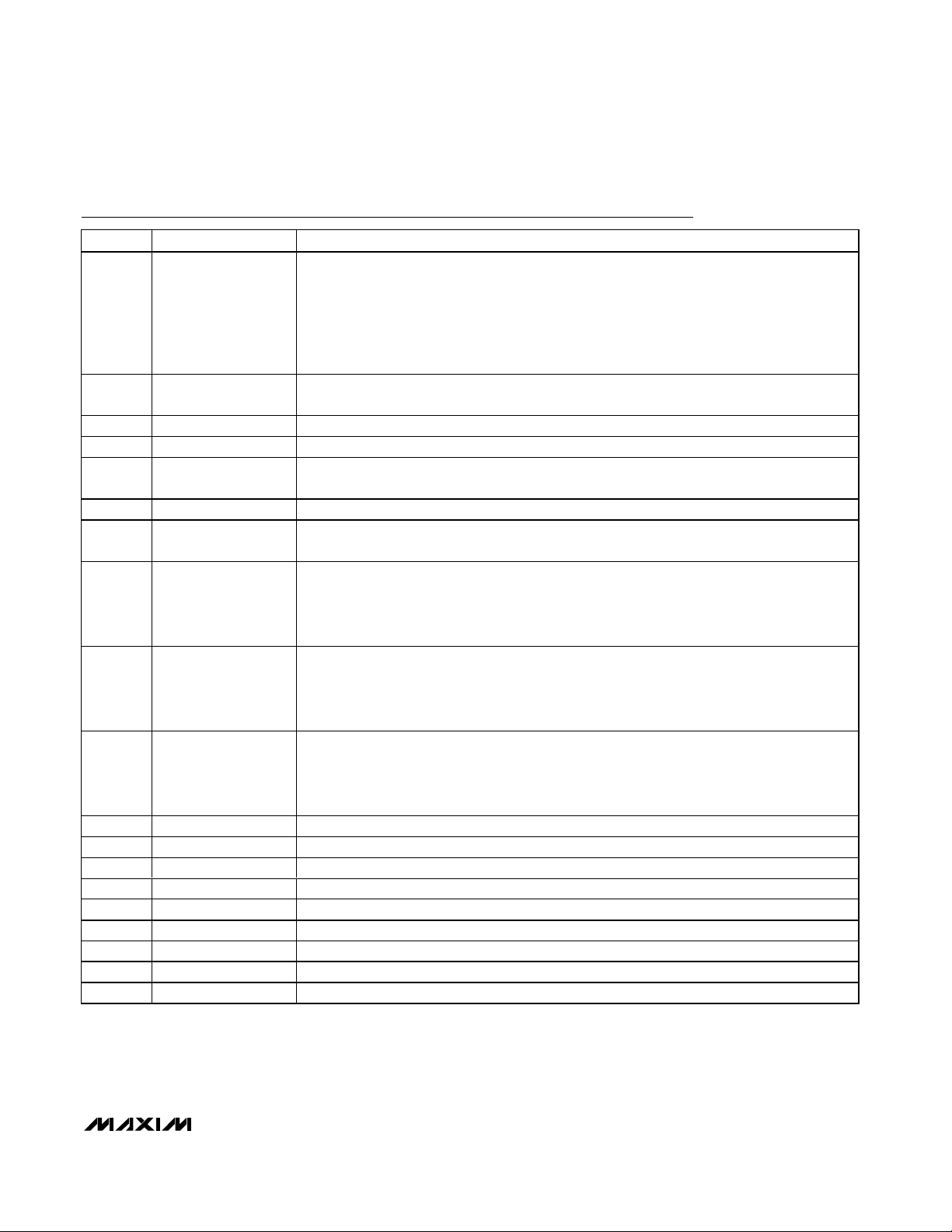
MAX2140
Complete SDARS Receiver
________________________________________________________________ Maxim Integrated Products 1
Ordering Information
19-3123; Rev 3; 10/05
For pricing, delivery, and ordering information, please contact Maxim/Dallas Direct! at
1-888-629-4642, or visit Maxim’s website at www.maxim-ic.com.
EVALUATION KIT
AVAILABLE
PART TEMP RANGE
PIN-PACKAGE
MAX2140ETH
-40°C to +85°C
44 Thin QFN-EP*
MAX2140ETH+
-40°C to +85°C
44 Thin QFN-EP*
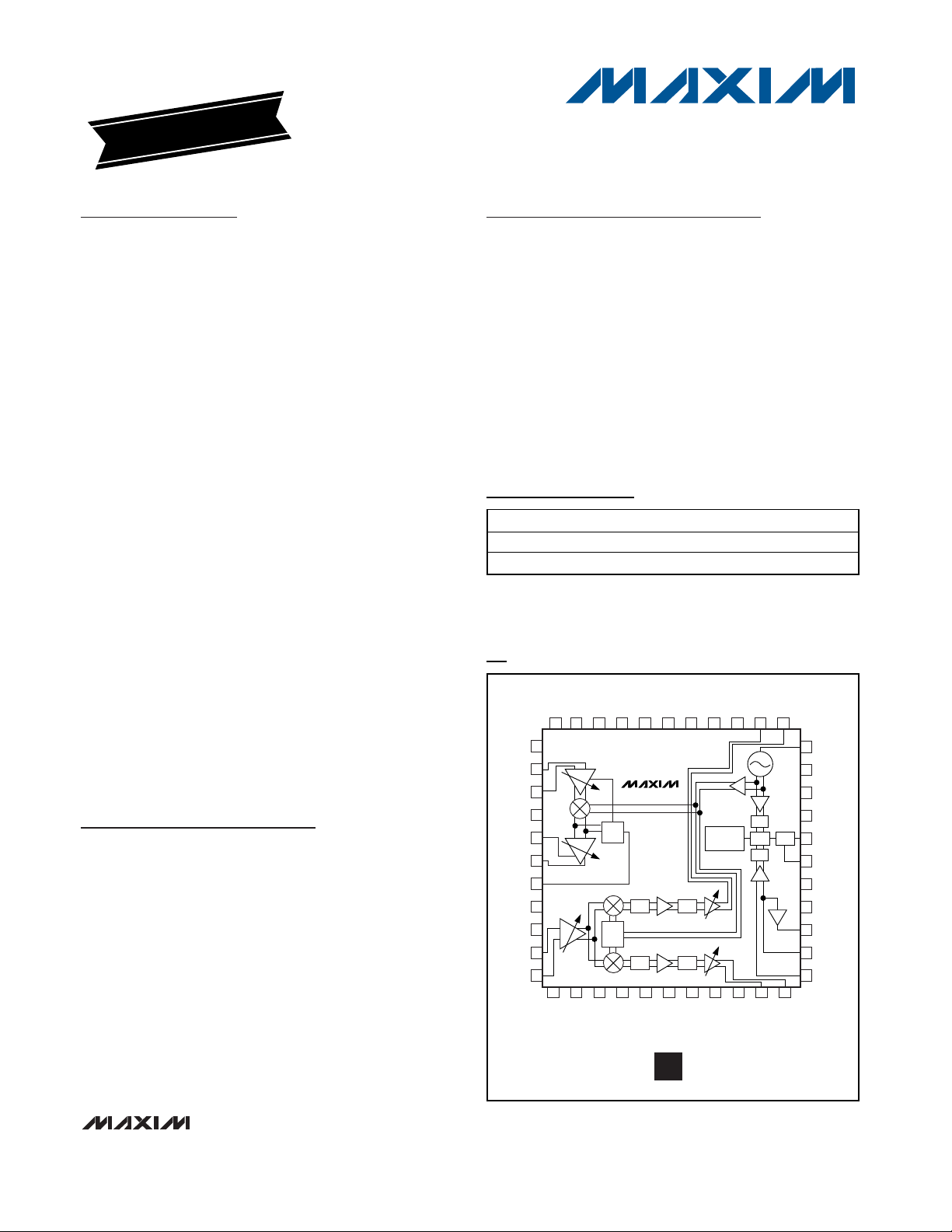
MAX2140
1
2
4
3
5
6
7
IF2QO-
SCL
IF2QI-
IF2QO+
RFAGC_C
VCC_FE0
RFIN-
XM TUNER
I
2
CA1
I
2
CA2
SDA
IFOUT-
IFOUT+
VCC_FE1
RFIN+
CHP
1/N
1/R
/4/8
QUAD
PFD
17
IF2II-
IF2IO+
IF2IO-
IF2II+
VINANT
VOUTANT
16
VCC_BE1
13 14 15
8
9
10
11
21
VCC_BE2
IOUT-
IOUT+
2019 2212 18
33
32
30
31
29
28
27
26
25
24
23
353637 3438394041424344
VCC_FE2
IFIN-
IFIN+
IF2QI+
VCC_FE3
QOUT-
QOUT+
VCC_D
VCC_BE4
VCC_A
LOCK
CPOUT
VCCREG
REFOUT
VCC_XTAL
XTAL
VTUNE
VCC_BE3
AGCPWM
LPF HPF
LPF HPF
RF
AGC
VCC_VCO
Σ Δ - MOD
ACTUAL SIZE
7mm x 7mm
Block Diagram/Pin Configuration
*EP = Exposed paddle.
+Denotes lead-free package.
Page 2
MAX2140
Complete SDARS Receiver
2 _______________________________________________________________________________________
ABSOLUTE MAXIMUM RATINGS
DC ELECTRICAL CHARACTERISTICS
(VCC= 3.1V to 3.6V; VINANT ≥ VCC, VOUTANT in open circuit, TA= -40°C to +85°C. Typical values are at VCC= 3.3V, VINANT =
3.3V, and T
A
= +25°C, unless otherwise noted.) (Note 1)
Stresses beyond those listed under “Absolute Maximum Ratings” may cause permanent damage to the device. These are stress ratings only, and functional
operation of the device at these or any other conditions beyond those indicated in the operational sections of the specifications is not implied. Exposure to
absolute maximum rating conditions for extended periods may affect device reliability.
V
CC_XX
to GND..................................................... -0.3V to +4.3V
VINANT to GND.................................................... -0.3V to +5.6V
AGCPWM to GND ................................................ -0.3V to +3.0V
Digital Input Current ........................................................ ±10mA
Maximum VSWR Without Damage ........................................ 4:1
Maximum VSWR Without Oscillations ................................... 4:1
All Other Pins ............................................... -0.3V to V
CC
+ 0.3V
Continuous Power Dissipation (T
A
= +70°C)
44-Pin TQFN (derate 26.31mW/°C above +70°C) ... 2105mW
Operating Temperature Range ..........................-40°C to +85°C
Junction Temperature .....................................................+150°C
Theta J
C
..........................................................................12°C/W
Storage Temperature Range ............................-65°C to +150°C
Lead Temperature (soldering, 10s) ................................+300°C
CAUTION! ESD SENSITIVE DEVICE
Supply Voltage Range (Note 2)
Operating Supply Current
Lock Indicator High (Locked) V
Lock Indicator Low (Unlocked) V
Digital Input-Logic High V
Digital Input-Logic Low V
Input Current for Digital Control
Pins
Input Current for AGCPWM I
Voltage Drop VINANT to
VOUTANT in Normal Operating
Mode
Current Sink at VOUTANT to Flag
Bit ACP = 1
Current Sink at VOUTANT to Flag
Bit AND = 1
PARAMETER SYMBOL CONDITIONS MIN TYP MAX UNITS
V
CC
VINANT 3.1 3.3 5.3
I
CC
I
SHDN
IH_LK
IL_LK
I
DIG
AGCPWM
V
ANTDC-
DROP
I
ANTDC_H
I
ANTDC_L
All blocks on 150 180 mA
All blocks off 30 µA
IH
IL
Maximum current sink at VOUTANT is
150mA
VOUTANT shorted to ground (Note 4) 195 500 mA
VCC - 0.5 V
VCC - 0.5 V
3.1 3.3 3.6
0.5 V
0.5 V
-1 +1 µA
-10 +290 µA
0.35 V
12 20 30 mA
V
Page 3
MAX2140
Complete SDARS Receiver
_______________________________________________________________________________________ 3
AC ELECTRICAL CHARACTERISTICS
(MAX2140 EV kit, current drawn at VOUTANT, I
VOUTANT
= 150mA max, VCC= 3.1V to 3.6V, VINANT = 3.1V to 5.3V, fRF= 2320MHz
to 2345MHz, f
LO
= 2076MHz, TA= -40°C to +85°C. Typical values are at VCC= VINANT = 3.3V, fRF= 2338MHz, TA= +25°C, unless
otherwise noted.) (Note 2)
Interstage (IF) 259MHz SAW filter specification: insertion loss = 19dB max, 9.3MHz to 12MHz from center attenuation = 24dB min,
beyond 12MHz from center attenuation = 40dB min.
GENERAL RECEIVER
Minimum Input RF Power to
Produce 20mV
I and Q Baseband Outputs
Maximum Input RF Power to
Produce 400mV
at I and Q Baseband Outputs
LO to RF Input Leakage
Noise Figure (Notes 3, 5) NF
In-Band Input IP3 (Notes 5, 6) I_IIP3
Out-of-Band Input IP3
(Notes 5, 7)
PARAMETER SYMBOL CONDITIONS MIN TYP MAX UNITS
(Differential) at
P-P
(Differential)
P-P
P
P
P
P
O_IIP3
MIN
MAX
LK_H
LK_L
IF AGC is set at maximum gain,
bit HPF = 0 (Note 4)
RF AGC threshold: RF_AGC_TRIP =
-17dBm; IF AGC is set at minimum gain, bit
HPF = 0
LO-related spurious > 2GHz -66
LO-related spurious < 2GHz -38
RF AGC is at maximum gain,
IF AGC is at reference gain
RF AGC is at maximum gain,
IF AGC is at reference gain -10dB
RF AGC is at maximum gain -5dB,
IF AGC is at reference gain
RF AGC is at maximum gain -10dB,
IF AGC is at reference gain
RF AGC is at maximum gain,
IF AGC is at reference gain
RF AGC is at maximum gain,
IF AGC is at reference gain -5dB
RF AGC is at maximum gain -30dB,
IF AGC is at reference gain -43dB
RF AGC is at maximum gain -20dB,
IF AGC is at reference gain -53dB
RF AGC is at maximum gain,
IF AGC is at reference gain
RF AGC is at maximum gain -7dB,
IF AGC is at reference gain
RF AGC is at maximum gain -25dB,
IF AGC is at reference gain
-91 -84 dBm
+3 dBm
8.5 10.4
9.3 11.7
13.3 15.5
17.8 21.5
-32
-27
+9
+6
-9
-3
+12
dBm
dB
dBm
dBm
Page 4
MAX2140
Complete SDARS Receiver
4 _______________________________________________________________________________________
AC ELECTRICAL CHARACTERISTICS (continued)
(MAX2140 EV kit, current drawn at VOUTANT, I
VOUTANT
= 150mA max, VCC= 3.1V to 3.6V, VINANT = 3.1V to 5.3V, fRF= 2320MHz
to 2345MHz, f
LO
= 2076MHz, TA= -40°C to +85°C. Typical values are at VCC= VINANT = 3.3V, fRF= 2338MHz, TA= +25°C, unless
otherwise noted.) (Note 2)
Interstage (IF) 259MHz SAW filter specification: insertion loss = 19dB max, 9.3MHz to 12MHz from center attenuation = 24dB min,
beyond 12MHz from center attenuation = 40dB min.
PARAMETER SYMBOL CONDITIONS MIN TYP MAX UNITS
In-Band Input IP2 (Notes 5, 6) I_IIP2
Out-of-Band Input IP2
(Notes 5, 7)
Opposite Sideband Rejection OSR Baseband frequencies = 100kHz (Note 4) 32 39 dB
Image Rejection IRej At f
Half IF Rejection HRej At fLO + 0.5 x f
RF AGC LOOP
LNA Gain Reduction
Minimum RF AGC Trip Point RFAGC_min Bits RF4/3/2/1/0 = 00000 (BIN) -35 dBm
RF AGC Trip Point RFAGC_int Bits RF4/3/2/1/0 = 00010 (BIN) (Note 4) -37 -33 -29 dBm
Maximum RF AGC Trip Point RFAGC_max Bits RF4/3/2/1/0 = 10100 (BIN) -15 dBm
FRONT-END (FE) PROGRAMMABLE GAIN
FE Programmable Gain Range FE_Rge (Note 4) 19 22 26 dB
FE Programmable Gain Step FE_Step 2 dB
IF FILTER INTERFACE
IF Output Differential Admittance Yout, IF
Input Differential Impedance
Presented by the IC to the IF
Filter Output
IF AGC LOOP
IF AGC Control Voltage for Max
Gain
IF AGC Control Voltage for Min
Gain
O_IIP2
RFAGC_
Range
Zin, IF
IFAGC_VM Applied at pin AGCPWM 0.2 V
IFAGC_Vm Applied at pin AGCPWM 2.5 V
RF AGC is at maximum gain,
IF AGC is at reference gain
RF AGC is at maximum gain,
IF AGC is at reference gain -5dB
RF AGC is at maximum gain,
IF AGC is at reference gain -25dB
RF AGC is at maximum gain,
IF AGC is at reference gain
RF AGC is at maximum gain -7dB,
IF AGC is at reference gain
RF AGC is at maximum gain -25dB,
IF AGC is at reference gain
- f
LO
IF
IF
(Note 4) 30 42 dB
Between pins IFOUT+, IFOUT-,
f
= 259MHz and 467MHz
IF
Between pins IFOUT+, IFOUT-,
f
= 259MHz and 467MHz
IF
+1
+6
+27
+38
+45
+60
54 dB
53 dB
1/900
+ j0
150
+ j0
dBm
dBm
S
Ω
Page 5

MAX2140
Complete SDARS Receiver
_______________________________________________________________________________________ 5
AC ELECTRICAL CHARACTERISTICS (continued)
(MAX2140 EV kit, current drawn at VOUTANT, I
VOUTANT
= 150mA max, VCC= 3.1V to 3.6V, VINANT = 3.1V to 5.3V, fRF= 2320MHz
to 2345MHz, f
LO
= 2076MHz, TA= -40°C to +85°C. Typical values are at VCC= VINANT = 3.3V, fRF= 2338MHz, TA= +25°C, unless
otherwise noted.) (Note 2)
Interstage (IF) 259MHz SAW filter specification: insertion loss = 19dB max, 9.3MHz to 12MHz from center attenuation = 24dB min,
beyond 12MHz from center attenuation = 40dB min.
IF AGC Gain-Control Range
INTERNAL BASEBAND LOWPASS FILTERS
LPF In-Band Ripple LPFA_rip
LPF Out-of-Band Rejection
(Note 4)
INTERNAL OUTPUT STAGE
Gain Increase BB_DG From bit HPF = 0 to HPF = 1 4 dB
Maximum I/QOUT± Pin Loading IQ_load Per each of the four pins 10//10 kΩ//pF
FREQUENCY GENERATION: VCO AND PLL
VCO Frequency Range
VCO Tuning Gain VCO_Gain (Note 4) 240 MHz/V
Synthesized VCO Phase Noise VCO_PN
Synthesized VCO Phase-Noise
Jitter
Charge-Pump Voltage Range V
Charge-Pump Current I
Pin CHP Leakage Current CHP_leak Across V
PLL Reference Division Ratio PLLref 1 2
Synthesized VCO Smallest
Fractional Step
PARAMETER SYMBOL CONDITIONS MIN TYP MAX UNITS
IFAGC_
LPFrej
LPFrej
VCO_
Range
VCO_jit
PLLstep Programmable through I
Rge
CHP
CHP
(Note 4) 47 64 dB
From 0 to 6.3MHz with respect to the
amplitude at 100kHz
At 10.25MHz with respect to the amplitude
at 2MHz
At 16MHz with respect to the amplitude at
2MHz
Over V
At 1kHz within PLL band -79
At 10kHz outside PLL band -80
At 100kHz outside PLL band -101
Integrated from 100Hz to 100kHz,
LO frequency = 2079MHz
Bit CHP = 0 0.6
Bit CHP = 1 1.2
range (Note 4) 1861 2079 MHz
CHP
range 5 nA
CHP
2
C23Hz
14 21
47 51
0.40 2.75 V
0.7 dB
dB
dBc/Hz
1.2 Deg
mA
RMS
Page 6

MAX2140
Complete SDARS Receiver
6 _______________________________________________________________________________________
AC ELECTRICAL CHARACTERISTICS (continued)
(MAX2140 EV kit, current drawn at VOUTANT, I
VOUTANT
= 150mA max, VCC= 3.1V to 3.6V, VINANT = 3.1V to 5.3V, fRF= 2320MHz
to 2345MHz, f
LO
= 2076MHz, TA= -40°C to +85°C. Typical values are at VCC= VINANT = 3.3V, fRF= 2338MHz, TA= +25°C, unless
otherwise noted.) (Note 2)
Interstage (IF) 259MHz SAW filter specification: insertion loss = 19dB max, 9.3MHz to 12MHz from center attenuation = 24dB min,
beyond 12MHz from center attenuation = 40dB min.
Note 1: At TA= -40°C, minimum and maximum values are guaranteed by design and characterization.
Note 2: Minimum and maximum values are guaranteed by design and characterization, unless otherwise noted.
Note 3: At T
A
= +25°C, minimum and maximum values are guaranteed by design and characterization.
Note 4: At T
A
= +25°C and TA= +85°C, parameters are production tested.
Note 5: IF AGC reference level is defined as being the required voltage applied on pin AGCPWM, and the corresponding receiver
IF gain, to measure 20mV
P-P
at each I/Q differential output when the RF input power is -91dBm. If even for zero volts
applied on pin AGCPWM the I/Q differential outputs are below 20mV
P-P
when the RF input power is -91dBm, then the refer-
ence level is defined as zero volts.
Note 6: In-band IP2 and IP3 are measured with two CW tones at RF input: f
1
= 2339.55MHz, f2= 2339.75MHz.
Note 7: Out-of-band IP2 and IP3 are measured with two CW tones at RF input: f
1
= 2326.25MHz, f2= 2330.25MHz.
Note 8: Error computed using a crystal with no error.
Note 9: No spur in the offset frequency range.
TIMING CHARACTERISTICS
Synthesized VCO Spurs VCOspur
XTAL Oscillator Frequency
Range
XTAL Oscillator Frequency Error XTALerror Using an external XTAL (Note 8) -16 +16 ppm
XTAL Oscillator Input Voltage XTALswing Using an external TCXO 0.8 V
XTAL Oscillator Input Duty Cycle XTALduty Using an external TCXO 47 50 53 %
Reference Buffer Output Voltage REFV
PARAMETER SYMBOL CONDITIONS MIN TYP MAX UNITS
XTALrge 24 49 MHz
0Hz < f
10kHz < f
1MHz < f
Using the REFOUT pin loading specified
below (Note 4)
< 10kHz (Note 9)
offset
< 1MHz (Note 9)
offset
< 10MHz -47
offset
0.95 1.10 V
CC
dBc
V
P-P
P-P
Reference Buffer Output Duty
Cycle
Maximum REFOUT Pin Loading REFOUT_1d
SERIAL INTERFACE (Note 2)
Serial Clock Frequency f
PARAMETER SYMBOL CONDITIONS MIN TYP MAX UNITS
REFduty
SCL
Using an external XTAL, not overdriven;
bit RFD = 0, using the REFOUT pin loading
specified below
REFOUT pin frequency = 24MHz 20
REFOUT pin frequency = 48MHz 8
45 50 55 %
200 kHz
pF
Page 7

MAX2140
Complete SDARS Receiver
_______________________________________________________________________________________ 7
Typical Operating Characteristics
(TA = +25°C, unless otherwise noted.)
INPUT RETURN LOSS
vs. FREQUENCY
MAX2140 toc01
FREQUENCY (GHz)
INPUT RETURN LOSS (dB)
2.42.3
-25
-20
-15
-10
-5
0
-30
2.2 2.5
MAXIMUM RF AGC
MINIMUM RF AGC
RF AGC ENGAGEMENT THRESHOLD
MAX2140 toc02
RF AGC ENGAGEMENT SETTING
RF AGC ENGAGEMENT THRESHOLD (dBm)
161284
-35
-30
-25
-20
-15
-10
-40
020
DIVIDER: /4
DIVIDER: /8
RF AGC ATTENUATION
vs. CONTROL VOLTAGE
MAX2140 toc03
CONTROL VOLTAGE (V)
RF AGC ATTENUATION (dB)
2.41.81.20.6
10
20
30
40
50
60
0
03.0
TA = +85°C
TA = +25°C
TA = -40°C
RF AGC SETTLING TIME
WITH 20dB STEP
MAX2140 toc04
START TIME: 0µs
STOP TIME: 200µs
RF AGC ATTACK
TIME
RF AGC DECAY
TIME
0dBm
5dB/div
-50dBm
IF AGC ATTENUATION
vs. CONTROL VOLTAGE
MAX2140 toc05
CONTROL VOLTAGE (V)
IF AGC ATTENUATION (dB)
2.41.81.20.6
10
20
30
40
50
60
70
0
03.0
R4 = 100Ω
C32 = 0.1µF
TA = +85°C
TA = +25°C
TA = -40°C
IF AGC ATTENUATION
vs. CONTROL VOLTAGE
MAX2140 toc06
CONTROL VOLTAGE (V)
IF AGC ATTENUATION (dB)
2.41.81.20.6
10
20
30
40
50
0
03.0
R4 = 5000Ω
C32 = 0.22µF
TA = +85°C
TA = +25°C
TA = -40°C
0dB
LPF FREQUENCY RESPONSE
10.250000MHz
-27.278dB
-100dB
1MHz 16MHz
MAX2140 toc07
Page 8

Typical Operating Characteristics (continued)
(TA = +25°C, unless otherwise noted.)
MAX2140
Complete SDARS Receiver
8 _______________________________________________________________________________________
LPF GROUP DELAY vs. FREQUENCY
REF
80ns
100ns/div
1MHz 16MHz
6.250000MHz
113.8ns
REFOUT WAVEFORM (REF = 1, RFD = 0)
MAX2140 toc08
-150dBc/Hz
VCO PHASE NOISE vs. OFFSET FREQUENCY
-50dBc/Hz
FREQUENCY OFFSET (Hz)
MAX2140 toc11
REFOUT WAVEFORM (REF = 0, RFD = 0)
MAX2140 toc09
500mV/div
1M10
REFOUT WAVEFORM (REF = 1, RFD = 1)
MAX2140 toc12
MAX2140 toc10
20ns/div
200mV/div
10ns/div
500mV/div
20ns/div
Page 9
MAX2140
Complete SDARS Receiver
_______________________________________________________________________________________ 9
Pin Description
PIN NAME FUNCTION
VCC_FE0, VCC_FE1,
1, 4, 8,
12–15, 23,
26, 27, 30,
31, 40
2, 3 RFIN+, RFIN-
5, 6 IFOUT+, IFOUT- Differential First IF Output. Connect an external SAW filter to the IF output.
7 RFAGC_C RF AGC Power-Detector Output. Set the RF AGC attack and decay response times.
9 AGCPWM
10, 11 IFIN+, IFIN- Differential First IF Input
16 VOUTANT
17, 19, 37,
39
18, 20, 36,38IF2II-, IF2II+, IF2QI+,
21, 22, 34,
35
24 XTAL Crystal Reference Input
25 REFOUT Buffered System Clock Output. Provides clock signal to the SDARS channel-decoder IC.
28 LOCK Digital Logic Output to the System Controller. Indicates the lock status of the internal PLL.
29 CPOUT VCO Charge-Pump Output
32 VCCREG Regulated Supply Voltage for the VCO
33 VTUNE High-Impedance VCO Tuning Input
41, 42 I2CA2, I2CA1 I2C Input Signals. Define the MAX2140 I2C device address.
43, 44 SCL, SDA I2C-Compatible Programming Input. Connect to an I2C-compatible bus.
— Exposed Pad Exposed Paddle. Connect to ground.
VCC_FE2, VCC_BE1,
VCC_BE2, VCC_BE3,
VINANT, VCC_XTAL,
VCC_D, VCC_A,
VCC_FE3, VCC_VCO,
VCC_BE4
IF2IO-, IF2IO+,
IF2QO+, IF2QO-
IF2QI-
IOUT-, IOUT+,
QOUT+, QOUT-
Power Supplies. Bypass to ground with capacitors as close to the pins as possible.
Differential RF Inputs. Accept RF input signal from the SDARS cabled antenna with a 50Ω to
100Ω balun.
IF AGC Control Voltage Input. Input from the filtered PWM AGC control signal from the SDARS
channel-decoder IC.
Overcurrent-Protected Unregulated DC Supply Output. Provides DC power supply to the
antenna module.
Differential Baseband DC Blocking Outputs.
IF2IO- = Inverting in-phase baseband output. AC couple to pin 18.
IF2IO+ = Noninverting in-phase baseband output. AC couple to pin 20.
IF2QO+ = Noninverting quadrature baseband output. AC couple to pin 36.
IF2QO- = Inverting quadrature baseband output. AC couple to pin 38.
Differential Baseband DC Blocking Inputs.
IF2II- = Inverting in-phase baseband input. AC couple to pin 16.
IF2II+ = Noninverting in-phase baseband input. AC couple to pin 19.
IF2QI+ = Noninverting quadrature baseband input. AC couple to pin 37.
IF2QI- = Inverting quadrature baseband input. AC couple to pin 39.
Differential I/Q Baseband Outputs.
IOUT- = Inverting in-phase baseband output.
IOUT+ = Noninverting in-phase baseband output.
QOUT+ = Noninverting quadrature baseband output.
QOUT- = Inverting quadrature baseband output.
Page 10

MAX2140
Complete SDARS Receiver
10 ______________________________________________________________________________________
Detailed Description
Front End
The front end of the MAX2140, which downconverts the
RF signal to IF, is defined from the differential RF inputs
(pins RFIN+ and RFIN-) to the output (pins IFOUT+ and
IFOUT-) to the SAW filter.
The front end includes a self-contained analog RF AGC
loop. The engagement threshold of the loop can be
programmed from -35dBm to -15dBm referred to the
RF input in 1dB steps using the RF4–RF0 programming
bits. The time constant of the loop is set externally by
the capacitor connected to RFAGC_C.
The image reject first mixer ensures a good image and
half IF rejection.
The front-end gain can be reduced by programming
bits PM3–PM0 over a 22dB range, with a step of 2dB.
This allows the selections of SAW filters with different
insertion loss.
The IF output is nominally 900Ω differentially and requires
pullup inductors to VCC, which can be used as part of the
matching network to the SAW filter impedance.
Back End
The back end, which downconverts the IF signal to
quadrature baseband, is defined from the SAW filter
inputs (pins IFIN+ and IFIN-) to the baseband outputs
(pins IOUT+, IOUT-, QOUT+, QOUT-).
The back end contains an IF AGC loop, which is closed
by the baseband controller. The IF AGC control voltage
is applied at the AGCPWM pin. The gain can be
reduced over 53dB (typ) and exhibits a log-linear characteristic.
The back end also contains individual lowpass filters on
each channel. The lowpass-filter bandwidth is the useful SDARS downconverted bandwidth (6.25MHz). The
lowpass-filter performance is factory trimmed. The bit
IOT switches between the factory-trimmed set and the
control through the I2C-compatible bus using bits
B4–B1. Even when using the factory-trimmed set, the
user can still slightly modify the cutoff frequency (by
±250kHz) by varying bits LP1/LP0.
Highpass filters are also inserted in the back-end signal
paths. Their purpose is to remove the DC offset. They
are designed for a low corner frequency so as not to
degrade the SDARS content. Their exact cutoff frequency is set by the external capacitors connected between
IF2 access pins, given by the following equation:
f
cutoff
= 1/(2 x π x R x C) [Hz]
where R = 8000Ω, C = external capacitor to be
connected.
Finally, the HPF bit allows an increase to the back-end
gain by 4dB at the slight expense of a degraded inband linearity.
Frequency Generation
An on-chip VCO and a low-step fractional-N PLL
ensure the necessary frequency generation. The 1st
mixer’s LO is at the VCO frequency itself, while the 2nd
mixer’s LO is the VCO frequency divided by 4 or by 8
(bit D48). Hence, the two possible IF frequencies for
SDARS are 467MHz and 259MHz. Typical applications
are based on 259MHz IF frequency.
The reference divider path in the PLL can either use an
external crystal and the on-chip crystal oscillator or an
external TCXO that can overdrive the on-chip crystal
oscillator. A reference division ratio of 1 or 2 is set by
the REF bit. The crystal oscillator (or TCXO) signal is
available at pin REFOUT. The output is either at the
same frequency as the reference signal, or divided by
two, based on the setting of bit RFD.
The VCO main division ratio is set by bits N6–N0 (for
the integer part) and bits F19–F00 (for the fractional
part). The minimum step is below 30Hz, small enough
for effective AFC to be implemented by the baseband.
The charge-pump (pin CPOUT) is to be connected to
the VCO tuning input (pin VTUNE) through an appropriate loop filter.
Overcurrent Protection
This DC function allows external circuitry consuming up
to 150mA and connected to the pin VOUTANT to sink
current from a VCCline (pin VINANT) through overcurrent-protection circuitry.
When no overcurrent is present, a low dropout voltage
exists between pins VINANT and VOUTANT. In overcurrent conditions (including short-circuit from
VOUTANT to GND), the current is limited to approximately 300mA and bit ACP in the READ byte status
goes high.
This circuit also senses if the current drawn at the pin
VOUTANT is typically larger than 20mA, in which case
the bit AND from the READ byte status goes high (the
purpose is to inform the baseband controller if there is
any device drawing current from VOUTANT).
Page 11

MAX2140
Complete SDARS Receiver
______________________________________________________________________________________ 11
Applications Information
Serial Interface and Control Registers
I2C Bit Description
MAX2140 Programming Bits:
The MAX2140 conforms to the Philips I2C standard,
400kbps (fast mode), and operates as a slave.
The MAX2140 addresses can be selected from three
values, which are determined by the logic state of the
two address-select pins I2CA1 and I2CA2. In all cases,
the MSB is transmitted (and read) first.
MAX2140 I
2
C-Compatible Programming Bit Definition:
BYTE PLLint:
RFD = reference buffer division: RFD = 0 (/1) and
RFD = 1 (/2)
N6 to N0 is the binary-written main dividing ratio,
integer part.
BYTE PLLfrac2:
PLS = Reserved: use only PLS = 0
LI1/0 = Reserved: use only LI1 = LI0 = 0
INT = Integer N mode: INT = 1 (fractional) and INT =
0 (integer)
Table 1. MAX2140 Write Address Bytes
Table 2. MAX2140 Read Address Bytes
Table 3. MAX2140 Write Programming Bits
AS1 AS0 MSB ADDRESS BYTE LSB
Low High 1 1 0 0 0 0 1 0
High Low 1 1 0 0 0 1 0 0
High High 1 1 0 0 0 1 1 0
AS1 AS0 MSB ADDRESS BYTE LSB
Low High 1 1 0 0 0 0 1 1
High Low 1 1 0 0 0 1 0 1
High High 1 1 0 0 0 1 1 1
WRITE-TO MODE RESET VALUE ADDR (hex) MSB CONTROL BYTE LSB
C2
Address —
PLLint 01010110 00 RFD N6 N5 N4 N3 N2 N1 N0
PLLfrac2 00011110 01 PLS LI1 LI0 INT F19 F18 F17 F16
PLLfrac1 10010000 02 F15 F14 F13 F12 F11 F10 F09 F08
PLLfrac0 01101001 03 F07 F06 F05 F04 F03 F02 F01 F00
Control 01100000 04 REF CHP D48 SDR ANT SDF SDB SDP
CustomGain 00000100 05 RF4 RF3 RF2 RF1 RF0 LP1 LP0 HPF
PMA_Test 00000000 06 PM3 PM2 PM1 PM0 SDX T2 T1 T0
LPFTrim 00000000 09 0 0 IOT B4 B3 B2A B2 B1
Unused2 00000000 08 0 00000 00
Unused1 00000000 07 0 00000 00
Unused0 00000000 10 0 00000 00
C4
C6
1
1
1
1
1
1
0
0
0
0
0
0
0
0
0
0
1
1
1
0
1
0
0
0
Page 12

MAX2140
Complete SDARS Receiver
12 ______________________________________________________________________________________
F19 to F16 is the upper-part binary-written main
dividing ratio, fractional part multiplied by 220=
1,048,576.
BYTES PLLfrac1 and PLLfrac0:
F15 to F0 is the lower-part binary-written main dividing ratio, fractional part multiplied by 2
20
= 1,048,576.
BYTE Control:
REF = reference division ratio: REF = 0 (/1) and REF
= 1 (/2)
CHP = charge-pump current: CHP = 0 (0.6mA) and
CHP = 1 (1.2mA)
D48 = LO division ratio: D48 = 0 (/4) and D48 = 1 (/8)
SDR = shutdown RF AGC: SDR = 0 (on) and SDR =
1 (shutdown)
ANT = antenna overcurrent protection: ANT = 0 (on)
and ANT = 1 (shutdown)
SDF = shutdown front end: SDF = 0 (on) and SDF =
1 (shutdown)
SDB = shutdown back end: SDB = 0 (on) and SDB =
1 (shutdown)
SDP = shutdown PLL: SDP = 0 (on) and SDP = 1
(shutdown)
BYTE CustomGain:
RF4/RF3/RF2/RF1/RF0 = RF AGC engagement
threshold (dBm): see the RF AGC Settling Time
graph in the Typical Operating Characteristics.
LP1/LP0 = change by 250kHz the LPF corner frequency: LP1/LP0 = 10 (nominal), LP1/LP0 = 11
(decrease), LP1/LP0 = 00 (increase)
HPF = HPF gain increase by 4dB: HPF = 0 (off) and
HPF = 1 (on)
BYTE PMA_Test:
PM3/PM2/PM1/PM0 = PMA gain cutback (dB):
PM3/PM2/PM1/PM0
DEC
SDX = shutdown reference buffer: SDX = 0 (on) and
SDX = 1 (shutdown)
T2/T1/T0 = test bits: 000 (normal), 001 (main division), 010 (reference division), 011 (reserved),
100 (CHP low-Z), 101 (CHP source on), 110 (CHP
sink on), 111 (CHP high-Z)
BYTE LPFTrim:
B4/B3/B2/B2A/B1 = Reserved for LPF trim. All = 0 in
normal operating mode
IOT = LPF corner frequency setup: IOT = 0 (default
factory trim) and IOT = 1 (controllable through I2C).
IOT = 0 in normal operating mode
BYTE Status:
RF AGC = RF AGC status: RF AGC = 0 (is not
engaged) and RF AGC = 1 (engaged)
ACP = antenna current protection: ACP = 0 (no overcurrent) and ACP = 1 (overcurrent)
AND = antenna detection: ANT = 0 (current < threshold) and ANT = 1 (current > threshold)
LD = lock detect: LD = 0 (out of lock) and LD = 1
(lock)
BYTE Reserved:
Inactive at this time, all bits are 0
Register configuration for the LO generation
when the comparison frequency = 23.92MHz:
to generate 2078.893333MHz:
PLLint = 01010110, PLLfrac2 = 00011110,
PLLfrac1= 10010000, PLLfrac0 = 01101001
to generate 2067.777778MHz:
PLLint = 01010110, PLLfrac2 = 00010111,
PLLfrac1 = 00100001, PLLfrac0 = 00000010
to generate 1871.004000 MHz:
PLLint = 01001110, PLLfrac2 = 00010011,
PLLfrac1 = 10000001, PLLfrac0 = 11111000
to generate 1861.000000MHz:
PLLint = 01001101, PLLfrac2 = 00011100,
PLLfrac1 = 11010000, PLLfrac0 = 11101000
Table 4. MAX2140 Read Programming Bits
READ-FROM MODE RESET VALUE ADDRESS (hex) MSB CONTROL BYTE LSB
C3
Address —
Reserved 00000000 00 0 0 0 0 0 0 0 0
Status 00000000 01 0 0 0 0 RFAGC ACP AND LD
C5
C7
1
1
1
1
1
1
0
0
0
0
0
0
0
0
0
0
1
1
1
0
1
1
1
1
Page 13
MAX2140
Complete SDARS Receiver
I2C Functional Description
I
2
C Register Map:
This is the standard I2C protocol. The first byte is either
C6, C4, C2 (hex) dependent on the state of the I
2
CA_
pins, for a write-to-device operation and either C7, C5,
C3 (hex) for a read-from operation (again dependent
on the state of pins I
2
CA_).
Write Operation:
The first byte is the device address plus the direction
bit (R/W = 0).
The second byte contains the internal address command of the first address to be accessed.
The third byte is written to the internal register directed
by the command address byte.
The following bytes (if any) are written into successive
internal registers.
The transfer lasts until stop conditions are encountered.
The MAX2140 acknowledges every byte transfer.
Read Operation:
When either address C3, C5, C7 is sent, the MAX2140
sends back first the status byte then the reserved byte.
See Table 5 and Table 6 for read/write register operations.
Layout Issues
The MAX2140 EV kit can be used as a starting point for
layout. For best performance, take into consideration
power-supply issues, as well as the RF, LO, and IF layout.
Power-Supply Layout
To minimize coupling between different sections of the
IC, the ideal power-supply layout is a star configuration,
which has a large decoupling capacitor at a central
V
CC
node. The VCCtraces branch out from this node,
each going to a separate V
CC
node in the MAX2140
circuit. At the end of each trace is a bypass capacitor
with impedance to ground less than 1Ω at the frequency of interest. This arrangement provides local decoupling at each V
CC
pin. Use at least one via per bypass
capacitor for a low-inductance ground connection.
Matching Network Layout
The layout of a matching network can be very sensitive
to parasitic circuit elements. To minimize parasitic
inductance, keep all traces short and place components as close to the IC as possible. To minimize parasitic capacitance, a cutout in the ground plane (and
any other planes) below the matching network components can be used. On the high-impedance ports (e.g.,
IF inputs and outputs), keep traces short to minimize
shunt capacitance.
Chip Information
TRANSISTOR COUNT: 22,000
PROCESS: BiCMOS
Table 5. Example: Write Registers 1 to 3 with 0E, D8, 26
Table 6. Example: Read from Status Registers (Sending an NACK Terminate Slave
Transmit Mode
Maxim cannot assume responsibility for use of any circuitry other than circuitry entirely embodied in a Maxim product. No circuit patent licenses are
implied. Maxim reserves the right to change the circuitry and specifications without notice at any time.
13 ____________________Maxim Integrated Products, 120 San Gabriel Drive, Sunnyvale, CA 94086 408-737-7600
© 2005 Maxim Integrated Products Printed USA is a registered trademark of Maxim Integrated Products, Inc.
Package Information
For the latest package outline information, go to
www.maxim-ic.com/packages
.
Device Address Write
(C2, C4, C6)
ACK Register Address 00 ACK DATA 0E ACK DATA D8 ACK DATA 26 ACK STOP
Device Address Write
(C2, C4, C6)
ACK Register Address 00 ACK DATA 0E ACK DATA D8 ACK DATA 26 ACK STOP
 Loading...