

Page 1
General Description
The MAX2130 broadband, low-distortion, low-noise,
two-output amplifier performs preamp, loop-out, and
buffer functions in TV tuner applications. The device
integrates functions typically achieved with discrete
components into the space-saving 8-pin µMAX-EP
package. The MAX2130 provides a gain of +15dB with
a noise figure less than 3.2dB over the 44MHz to
878MHz frequency range. The MAX2130 features an
externally adjustable bias control, set with a single
resistor, that allows the user to meet minimum linearity
requirements while reducing current consumption. The
device operates from a +5V single supply and only
requires 93mA of supply current when nominally
biased.
________________________Applications
DVB-T Digital Broadcast Receivers
Digital/Terrestrial TV Tuners
Set-Top Boxes
Cable Modems
Analog TV Tuners
Features
♦ +5V Single-Supply Operation
♦ 44MHz to 878MHz Operating Frequency Range
♦ Guaranteed 7.4dB (min) Input Return Loss Over
Frequency Range
♦ LNA Performance at I
CC
= 93mA (R
BIAS
= 15kΩ)
15dB Gain
2.8dB Noise Figure
+17.5dBm Input IP3
+27dBm Input IP2
+2.7dBm Input 1dB Compression Point
♦ Loop-Out Amplifier Performance at I
CC
= 93mA
(R
BIAS
= 15kΩ)
8.7dB Gain
4.2dB Noise Figure
+17dBm Input IP3
+29dBm Input IP2
-0.5dBm Input 1dB Compression Point
♦ Programmable Linearity vs. Supply Current
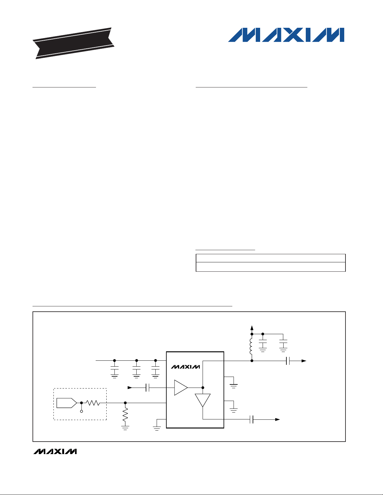
MAX2130
Broadband, Two-Output, Low-Noise
Amplifier for TV Tuner Applications
________________________________________________________________ Maxim Integrated Products 1
MAX2130
47pF1000pF10μF
V
CC
V
CC
IN
BIAS
OUT1
GND
GND
OUT2
INPUT
0.1μF
DAC
V
ADJ
R
ADJ
R
BIAS
15kΩ
1.2V
220pF 1000pF
V
CC
0.1μF
LNA
OUTPUT
0.1μF
LOOP-OUT
OUTPUT
OPTIONAL: DYNAMIC
LINEARITY ADJUSTMENT CIRCUIT
CHOKE
MURATA
BLM11A221S
GND
Typical Application Circuit
19-1806; Rev 1; 8/03
Ordering Information
*Exposed paddle
Pin Configuration appears at end of data sheet.
PART TEMP RANGE PIN-PACKAGE
MAX2130EUA -40°C to +85°C 8 µMAX-EP*
EVALUATION KIT
AVAILABLE
For pricing, delivery, and ordering information, please contact Maxim/Dallas Direct! at
1-888-629-4642, or visit Maxim’s website at www.maxim-ic.com.
Page 2
MAX2130
Broadband, Two-Output, Low-Noise
Amplifier for TV Tuner Applications
2 _______________________________________________________________________________________
ABSOLUTE MAXIMUM RATINGS
DC ELECTRICAL CHARACTERISTICS
(VCC= +4.75V to +5.25V, TA= -40°C to +85°C, R
BIAS
= 15kΩ
±1%; no input signals applied. Typical values are at V
CC
= +5V,
T
A
= +25°C, unless otherwise noted.)
AC ELECTRICAL CHARACTERISTICS
(MAX2130 EV kit, VCC= +4.75V to +5.25V, RBIAS = 15kΩ ±1%, fIN= 500MHz, ZO= 75Ω. Typical values are at VCC= +5V,
T
A
= +25°C, unless otherwise noted.) (Note 1)
Stresses beyond those listed under “Absolute Maximum Ratings” may cause permanent damage to the device. These are stress ratings only, and functional
operation of the device at these or any other conditions beyond those indicated in the operational sections of the specifications is not implied. Exposure to
absolute maximum rating conditions for extended periods may affect device reliability.
VCCto GND..............................................................-0.3V to +6V
BIAS, OUT2 to GND .....................................-0.3 to (V
CC
+ 0.3V)
IN Input Power................................................................+15dBm
OUT1 to GND ...........................................................-0.3V to +6V
OUT2 Short-Circuit Duration ......................................Continuous
Continuous Power Dissipation (T
A
= +70°C)
8-Pin µMAX-EP (derate 15.4mW/°C above +70°C) ........1.2W
Operating Temperature Range ...........................-40°C to +85°C
Junction Temperature......................................................+150°C
Storage Temperature Range .............................-65°C to +150°C
Lead Temperature (soldering, 10s) .................................+300°C
PARAMETER CONDITIONS
MIN
TYP
MAX
UNITS
Supply Voltage
V
TA = +25°C 93 104
R
BIAS
= 30kΩ 49
Supply Current
BIAS = unconnected 10
mA
CAUTION! ESD SENSITIVE DEVICE
4.75 5.25
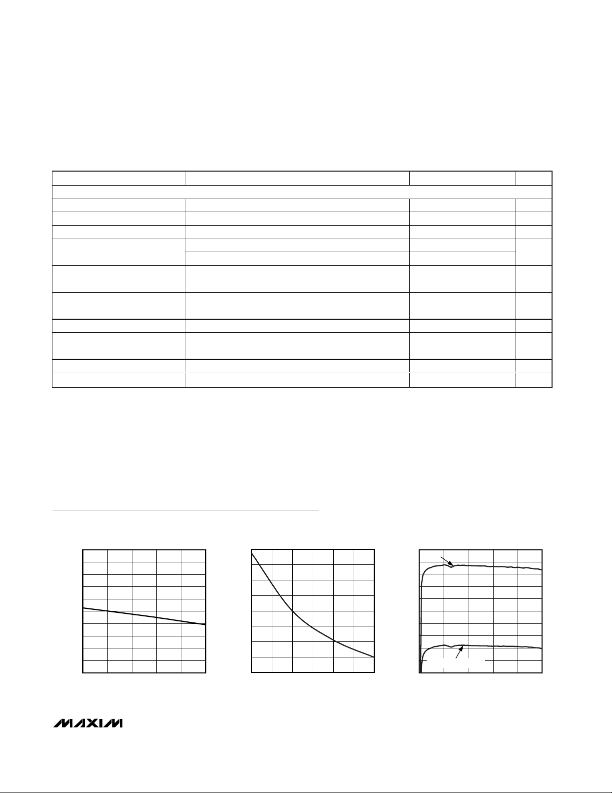
PARAMETER CONDITIONS MIN TYP MAX UNITS
LOW-NOISE AMPLIFIER (LNA)
Operating Frequency Range 44 878 MHz
Gain (Note 2) 13.4 15 16.6 dB
Gain Flatness TA = -40°C to +85°C (Note 2) 0.8 dB
Noise Figure 2.8 3.2 dB
Input 1dB Compression Point
Inp ut Thi r d - Or d er Inter cep t P oi nt (Note 4) 17.5 dBm
Input Second-Order Intercept
Point
IN Return Loss (Notes 2, 6) 7.4 8.6 dB
OUT1 Return Loss fIN = 44MHz to 878M H z 8.7 dB
Maximum Load for Stable
Operation
OUT1 to IN Isolation (Note 2) 18 21 dB
V
= +3.5V (Note 3) 2.1
CC
(Note 5) 27 dBm
2.7
Any load
dBm
Page 3
MAX2130
Broadband, Two-Output, Low-Noise
Amplifier for TV Tuner Applications
_______________________________________________________________________________________ 3
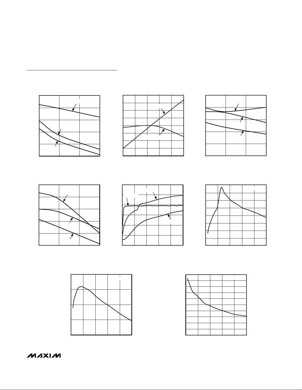
88
91
90
89
92
93
94
95
96
97
98
-40 10-15 35 60 85
SUPPLY CURRENT vs. TEMPERATURE
MAX2130 toc01
TEMPERATURE (°C)
SUPPLY CURRENT (mA)
50
60
70
80
90
100
110
120
130
10.0 15.012.5 17.5 20.0 22.5 25.0
SUPPLY CURRENT vs. R
BIAS
MAX2130 toc02
R
BIAS
(kΩ)
SUPPLY CURRENT (mA)
7
10
9
8
11
12
13
14
15
16
17
0 400200 600 800 1000
GAIN vs. FREQUENCY
R
BIAS
= 10kΩ
MAX2130 toc03
FREQUENCY (MHz)
GAIN (dB)
LOOP-OUT AMPLIFIER
LNA
AC ELECTRICAL CHARACTERISTICS (continued)
(MAX2130 EV kit, VCC= +4.75V to +5.25V, RBIAS = 15kΩ ±1%, fIN= 500MHz, ZO= 75Ω. Typical values are at VCC= +5V,
T
A
= +25°C, unless otherwise noted.) (Note 1)
Note 1: Specifications are guaranteed by design and characterization, except for gain which is production tested.
Note 2: Specifications are guaranteed over the operating frequency range.
Note 3: Operation possible with V
CC
= +3.5V. See Typical Operating Characteristics.
Note 4: Two tones at 500MHz and 506MHz, -20dBm per tone.
Note 5: Two tones at 500MHz and 550MHz, -20dBm per tone.
Note 6: Output load has worst-case 6dB return loss.
PARAMETER CONDITIONS
MIN
TYP
MAX
UNITS
LOOP-OUT AMPLIFIER
Operating Frequency Range 44 878
MHz
Gain (Note 2) 7.1 8.7
dB
Noise Figure 4.2 4.6 dB
-0.5
Input 1dB Compression
Point
V
CC
= +3.5V (Note 3) -3.7
dBm
Input Third-Order Intercept
Point
(Note 4) 17
dBm
Input Second-Order Intercept
Point
(Note 5) 29
dBm
OUT2 Return Loss fIN = 44MHz to 878M H z
dB
Maximum Load for Stable
Operation
OUT2 to IN Isolation (Note 2)
27 dB
OUT2 to OUT1 Isolation (Note 2)
dB
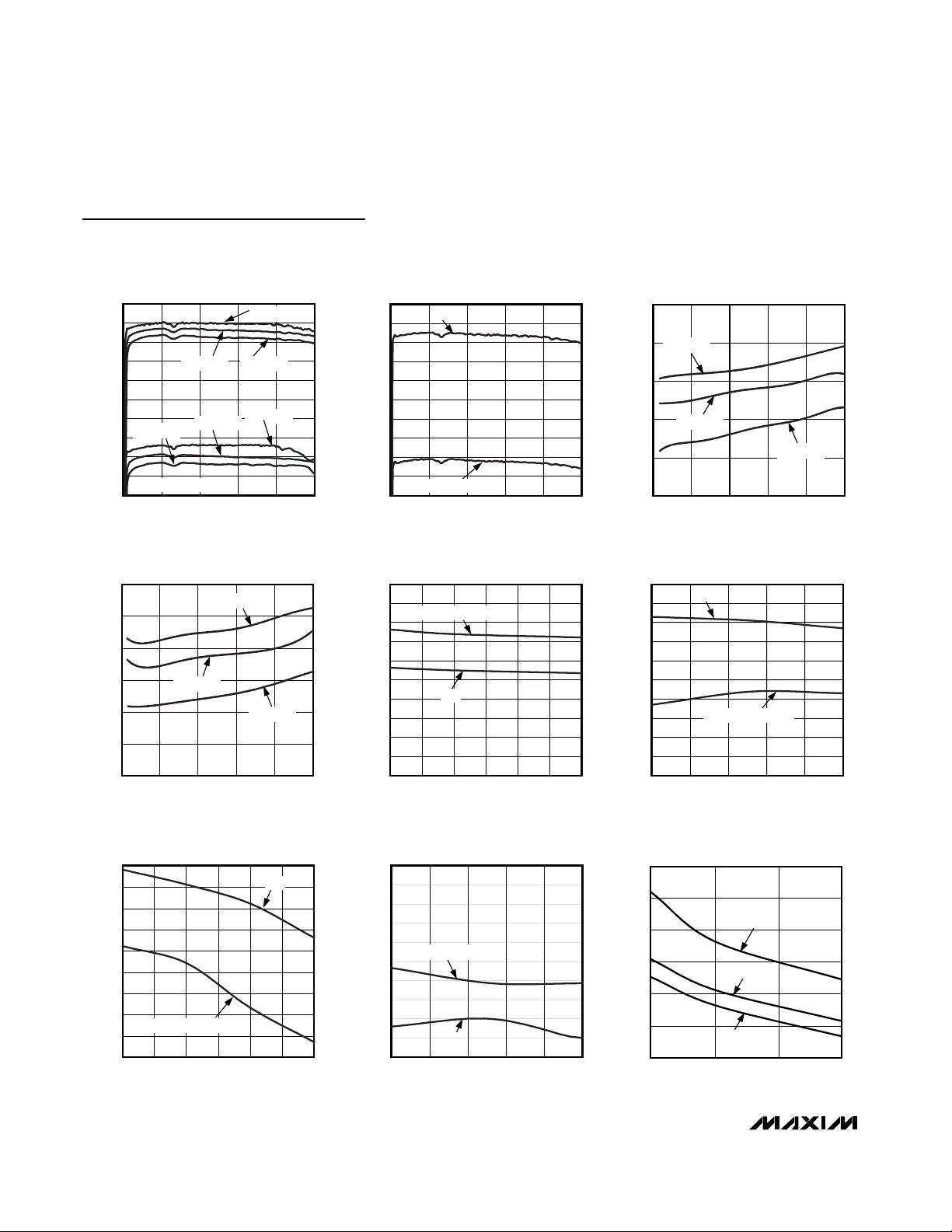
Typical Operating Characteristics
(MAX2130 EV kit, VCC= +5V, R
BIAS
= 15kΩ ±1%, TA = +25°C, unless otherwise noted.)
10.2
16.6
Any load
24.5
11.0 12.5
Page 4
MAX2130
Broadband, Two-Output, Low-Noise
Amplifier for TV Tuner Applications
4 _______________________________________________________________________________________
Typical Operating Characteristics (continued)
(MAX2130 EV kit, VCC= +5V, R
BIAS
= 15kΩ ±1%, TA = +25°C, unless otherwise noted.)
7
10
9
8
11
12
13
14
15
16
17
0 400200 600 800 1000
GAIN vs. FREQUENCY
R
BIAS
= 15kΩ
MAX2130 toc04
FREQUENCY (MHz)
GAIN (dB)
LNA
LOOP-OUT AMPLIFIER
TA = -40°C
TA = +25°C
TA = +85°C
TA = -40°C
TA = +85°C
TA = +25°C
7
10
9
8
11
12
13
14
15
16
17
0 400200 600 800 1000
GAIN vs. FREQUENCY
R
BIAS
= 25kΩ
MAX2130 toc05
FREQUENCY (MHz)
GAIN (dB)
LOOP-OUT AMPLIFIER
LNA
0
1
3
2
4
5
0 400200 600 800 1000
LNA NOISE FIGURE vs. FREQUENCY
MAX2130 toc06
FREQUENCY (MHz)
NOISE FIGURE (dB)
TA = +85°C
TA = +25°C
TA = -40°C
0
2
1
4
3
5
6
0 400200 600 800 1000
LOOP-OUT AMPLIFIER
NOISE FIGURE vs. FREQUENCY
MAX2130 toc07
FREQUENCY (MHz)
NOISE FIGURE (dB)
TA = +25°C
TA = -40°C
TA = +85°C
0
1.5
1.0
0.5
2.0
2.5
3.0
3.5
4.0
4.5
5.0
10.0 15.012.5 17.5 20.0 22.5 25.0
NOISE FIGURE vs. R
BIAS
MAX2130 toc08
R
BIAS
(kΩ)
NOISE FIGURE (dB)
LNA
LOOP-OUT AMPLIFIER
-5
-2
-3
-4
-1
0
1
2
3
4
5
-40 10-15 35 60 85
INPUT P1dB vs. TEMPERATURE
MAX2130 toc09
TEMPERATURE (°C)
INPUT P1dB (dBm)
LNA
LOOP-OUT AMPLIFIER
-5
-3
-4
0
-1
-2
3
2
1
4
10.0 15.012.5 17.5 20.0 22.5 25.0
INPUT P1dB vs. R
BIAS
MAX2130 toc10
R
BIAS
(kΩ)
INPUT P1dB (dBm)
LNA
LOOP-OUT AMPLIFIER
25
28
27
26
29
30
31
32
33
34
35
-40 10-15 35 60 85
INPUT IP2 vs. TEMPERATURE
MAX2130 toc11
TEMPERATURE (°C)
INPUT IP2 (dBm)
LNA
LOOP-OUT AMPLIFIER
15
25
20
35
30
40
45
10 15 20 25
MAX2130 toc12
R
BIAS
(kΩ)
INPUT IP2 (dBm)
LNA
INPUT IP2 vs. R
BIAS
100MHz
600MHz
800MHz
Page 5
MAX2130
Broadband, Two-Output, Low-Noise
Amplifier for TV Tuner Applications
_______________________________________________________________________________________ 5
15.0
15.5
16.0
16.5
17.0
17.5
18.0
18.5
19.0
-40 -15 10 35 60 85
INPUT IP3 vs. TEMPERATURE
MAX2130-14
TEMPERATURE (°C)
INPUT IP3 (dBm)
LOOP-OUT AMPLIFIER
LNA
10
12
16
14
18
20
MAX2130 toc15
R
BIAS
(kΩ)
INPUT IP3 (dBm)
10 2015 25
LNA
INPUT IP3 vs. R
BIAS
600MHz
800MHz
100MHz
10
12
16
14
18
20
MAX2130 toc16
R
BIAS
(kΩ)
INPUT IP3 (dBm)
10 2015 25
LOOP-OUT AMPLIFIER
INPUT IP3 vs. R
BIAS
600MHz
800MHz
100MHz
-60
-40
-50
-20
-30
-10
0
0 400200 600 800 1000
ISOLATION vs. FREQUENCY
MAX2130 toc17
FREQUENCY (MHz)
ISOLATION (dB)
OUT2 TO OUT1
OUT1 TO IN
OUT2 TO IN
0
15
5
25
20
35
30
40
0 400200 600 800 1000
IN PORT
RETURN LOSS vs. FREQUENCY
MAX2130 toc18
FREQUENCY (MHz)
RETURN LOSS (dB)
10
ZO = 75Ω
20
15
10
5
0
0 400200 600 800 1000
OUT1 PORT
RETURN LOSS vs. FREQUENCY
MAX2130 toc19
FREQUENCY (MHz)
RETURN LOSS (dB)
ZO = 75Ω
0
15
10
5
20
25
30
35
40
45
50
0 400200 600 800 1000
OUT2 PORT
RETURN LOSS vs. FREQUENCY
MAX2130 toc20
FREQUENCY (MHz)
RETURN LOSS (dB)
ZO = 75Ω
20
25
35
30
40
45
MAX2130 toc13
R
BIAS
(kΩ)
INPUT IP2 (dBm)
10 2015 25
LOOP-OUT AMPLIFIER
INPUT IP2 vs. R
BIAS
100MHz
600MHz
800MHz
Typical Operating Characteristics (continued)
(MAX2130 EV kit, VCC= +5V, R
BIAS
= 15kΩ ±1%, TA = +25°C, unless otherwise noted.)
Page 6
MAX2130
Broadband, Two-Output, Low-Noise
Amplifier for TV Tuner Applications
6 _______________________________________________________________________________________
Detailed Description
The MAX2130 is a broadband, high-gain, low-distortion
low-noise amplifier (LNA) with two outputs intended for
operation over the 44MHz to 878MHz frequency range.
The device operates from a +5V supply and features
externally adjustable bias control circuitry that allows
minimum linearity requirements to be met while reducing current consumption.
Input
The IN port is a broadband 75Ω input that provides a
guaranteed minimum input return loss of 7.4dB (allowing for 2:1 VSWR at output) across the 44MHz to
878MHz frequency range. AC-couple the IN port with a
0.1µF DC-blocking capacitor.
Outputs
The OUT1 port is a broadband, 75Ω, open-collector
output for the LNA. It requires a pullup inductor to V
CC
for proper biasing, as well as a 0.1µF DC-blocking
capacitor. See the Applications Information section for
proper inductor selection.
The OUT2 port is a broadband, 75Ω output for the loopout amplifier. The loop-out amplifier is internally biased
and does not require a pullup inductor. AC-couple the
OUT2 port with a 0.1µF DC-blocking capacitor.
Bias Circuitry
The linearity and supply current for both amplifiers are
externally programmable with a single resistor, R
BIAS
,
from BIAS to GND. A nominal resistor value of 15kΩ
sets an input IP3 of +17.5dBm, an input IP2 of
+27dBm, and a supply current of 93mA. Decrease the
resistor value to improve linearity at the cost of
increased supply current. Increase the resistor value to
decrease supply current and degrade linearity. Use
resistor values greater than 10kΩ. Gain is not significantly affected by the R
BIAS
value.
Applications Information
Inductor Selection
The OUT1 port of the LNA requires a pull-up inductor to
VCCfor proper biasing. The exact value of the inductor
is not important as long as it has broadband impedance >150Ω (<500Ω) at 10MHz across the 44MHz to
878MHz frequency band. Table 1 is a list of recommended inductors.
Pin Description
PIN NAME FUNCTION
1V
CC
Supply Voltage Input. Bypass with a 1000pF capacitor in parallel with a 47pF capacitor as close to
the pin as possible. (See Typical Application Circuit.)
2IN
Broadband Input to Low-Noise Amplifier and Loop-Out Amplifier. Internally matched to 75Ω.
Requires 0.1μF DC-blocking capacitor. (See Typical Application Circuit.)
3 BIAS
Bias-Setting Resistor Connection. Connect a resistor, R
BIAS
, from BIAS to GND to set the linearity
and supply current of the LNA and the loop-out amplifier.
4, 6, 7, EP
GND
Ground. Connect to ground plane with a low-inductance connection. Solder exposed paddle evenly
to the board groundplane.
5 OUT2
Output of Loop-Out Amplifier. Requires a 0.1μF DC-blocking capacitor. (See Typical Application
Circuit.)
8 OUT1
Open-Collector Output of Low-Noise Amplifier. Requires a pullup inductor to V
CC
, as well as a 0.1μF
DC-blocking capacitor. (See Typical Application Circuit.)
Table 1. OUT1 Pullup Inductor
Recommended Components
PART NUMBER MANUFACTURER
BLM11A221S Murata
BLM11A471SG Murata
BLM10A221SG Murata
BLM21A331SG Murata
Page 7
Dynamic Linearity Adjustment
The LNA and loop-out amplifier linearity can be dynamically adjusted by varying the amount of current
sourced by the BIAS port. The BIAS port is internally
biased to 1.2V. A resistor, R
BIAS
, connected from BIAS
to ground sets the bias current. An additional resistor,
R
ADJ
, placed from the BIAS port to an external voltage
source, such as a digital-to-analog converter (DAC),
varies the current sourced by the BIAS port. Choosing
R
ADJ
= R
BIAS
= 20kΩ and varying the voltage of the
DAC from ground to 2.4V effectively varies the resistance seen from the BIAS port from 10kΩ to an open
circuit. See Typical Application Circuit.
The DAC output voltage, V
ADJ
, required to set an equivalent resistance to ground, REQ, seen by the BIAS port,
can be calculated with the following equation:
V
ADJ
= 2.4V - (R
BIAS
✕
V
BIAS
) / R
EQ
where R
ADJ
= R
BIAS
, V
BIAS
= 1.2V, REQ≥ 10kΩ.
Power-Supply Bypassing
Proper voltage-supply bypassing is essential for highfrequency circuit stability. Bypass the VCCpin with a
1000pF capacitor in parallel with a 47pF capacitor,
located as close to the VCCpin as possible. Refer to
the MAX2130 EV kit for additional information.
MAX2130
Broadband, Two-Output, Low-Noise
Amplifier for TV Tuner Applications
_______________________________________________________________________________________ 7
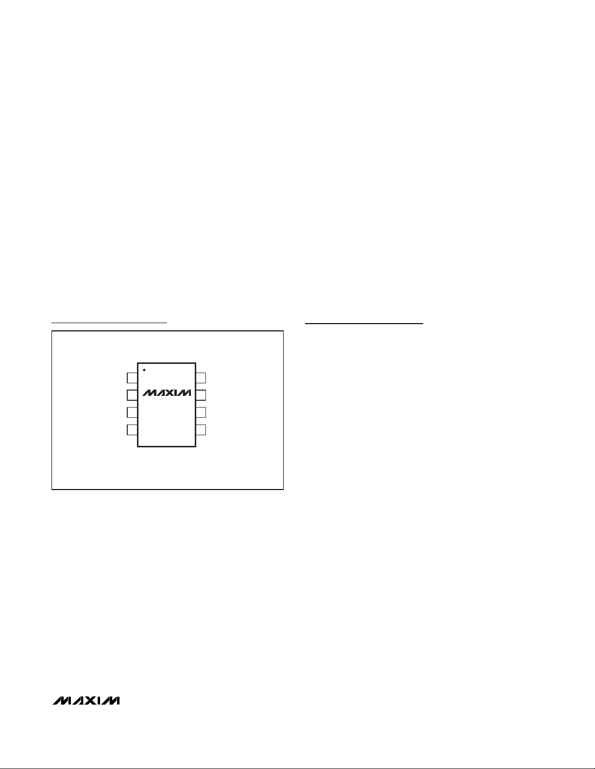
GND
OUT2GND
1
2
87OUT1
GNDIN
BIAS
V
CC
μMAX-EP
TOP VIEW
3
4
6
5
MAX2130
Pin Configuration
Chip Information
TRANSISTOR COUNT: 167
Page 8

MAX2130
Broadband, Two-Output, Low-Noise
Amplifier for TV Tuner Applications
Maxim cannot assume responsibility for use of any circuitry other than circuitry entirely embodied in a Maxim product. No circuit patent licenses are
implied. Maxim reserves the right to change the circuitry and specifications without notice at any time.
8 _____________________Maxim Integrated Products, 120 San Gabriel Drive, Sunnyvale, CA 94086 408-737-7600
© 2003 Maxim Integrated Products Printed USA is a registered trademark of Maxim Integrated Products.
8L, μMAX, EXP PAD.EPS
C
1
1
21-0107
Package Information
(The package drawing(s) in this data sheet may not reflect the most current specifications. For the latest package outline information
go to www.maxim-ic.com/packages
.)
 Loading...