________________General Description
The MAX212 RS-232 transceiver is intended for 3V-powered EIA/TIA-232E and V.28/V.24 communication interfaces where 3 drivers and 5 receivers are needed with
minimum power consumption. The operating voltage
range extends from 3.6V down to 3.0V while still maintaining true RS-232 and EIA/TIA-562 voltage levels.
A 1µA typical shutdown mode reduces power consumption, extending battery life in portable systems.
While shut down, all receivers can remain active or can
be disabled under logic control. This enables a system
incorporating the CMOS MAX212 to be in low-power
shutdown mode and monitor incoming RS-232 activity.
A guaranteed data rate of 120kbps provides compatibility with popular software for communicating with personal computers.
Three-state drivers on all receiver outputs are provided
so that multiple receivers, generally of different interface standards, can be wire-ORed at the UART.
The MAX212 is available in both small-outline (SO) and
shrink-small-outline (SSOP) packages. The SSOP
package occupies less than half of the board area
required by the equivalent SO package.
________________________Applications
Computers
Notebooks/Palmtops/Subnotebooks
Printers
Peripherals
Instruments
____________________________Features
SUPERIOR TO BIPOLAR:
♦ Operates from Single +3.0V to +3.6V Supply
♦ 24-Pin SSOP or Wide SO Packages
♦ Meets All EIA/TIA-232E & EIA/TIA-562
Specifications
♦ 3mA Max Supply Current (Unloaded)
♦ 1µA Low-Power Shutdown Mode
♦ All Receivers Active During Low-Power Shutdown
♦ Mouse Compatible at 3.0V
♦ Low-Cost, Surface-Mount External Components
♦ 120kbps Guaranteed Data Rate—LapLink™
Compatible
♦ Three-State Receiver Outputs
♦ Evaluation Kit Available
♦ Flow-Through Pinout
MAX212
+3V-Powered, Low-Power,
True RS-232 Transceiver
________________________________________________________________
Maxim Integrated Products
1
Call toll free 1-800-998-8800 for free samples or literature.
PART TEMP. RANGE PIN-PACKAGE
MAX212CWG 0°C to +70°C 24 Wide SO
MAX212CAG 0°C to +70°C 24 SSOP
MAX212C/D 0°C to +70°C Dice*
MAX212EAG -40°C to +85°C 24 SSOP
MAX212EWG -40°C to +85°C 24 Wide SO
EV KIT TEMP. RANGE BOARD TYPE
MAX212EVKIT-SSOP 0°C to +70°C Surface Mount
19-0162; Rev 2; 2/94
™LapLink is a registered trademark of Traveling Software.
_______________Ordering Information
* Dice are tested at TA= +25°C only.
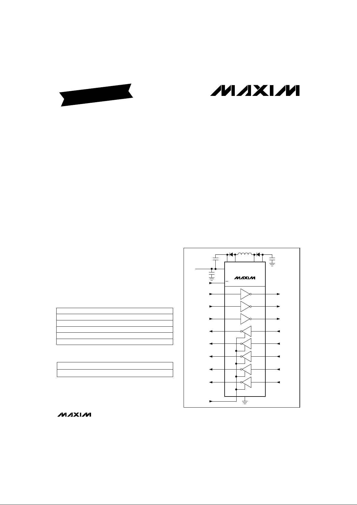
___________T ypical Operating Circuit
MAX212
T1
IN
V
CC
SD
+3.3V
DC-DC CONVERTER
EN
T1
OUT
LN
LP V-V+
GND
1
21423
T1
SHUTDOWN
11
3
4
17
T2
IN
T2
OUT
T2
12 16
T3
IN
T3
OUT
T3
13 15
R1
OUT
R1
IN
622
R2
OUT
R2
IN
R2
721
R3
OUT
R3
IN
820
R3
R4
OUT
R4
IN
919
R4
R5
OUT
R5
IN
10 18
R5
5
24
ENABLE
R1
EVALUATION KIT
INFORMATION INCLUDED

MAX212
+3V-Powered, Low-Power,
True RS-232 Transceiver
2 _______________________________________________________________________________________
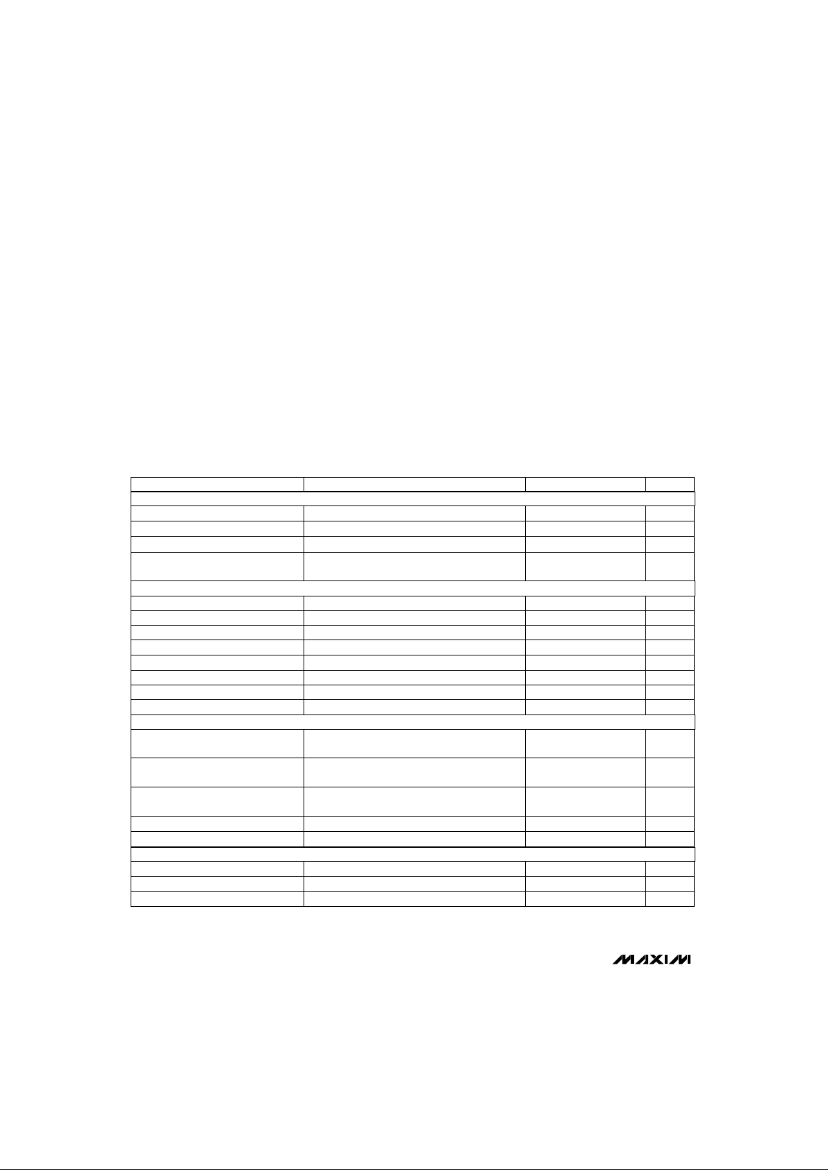
ABSOLUTE MAXIMUM RATINGS
ELECTRICAL CHARACTERISTICS
(VCC= 3.0V to 3.6V, TA= T
MIN
to T
MAX
, unless otherwise noted.)
Stresses beyond those listed under “Absolute Maximum Ratings” may cause permanent damage to the device. These are stress ratings only, and functional
operation of the device at these or any other conditions beyond those indicated in the operational sections of the specifications is not implied. Exposure to
absolute maximum rating conditions for extended periods may affect device reliability.
PARAMETER MIN TYP MAX UNITS
Input Logic Threshold Low V
CC
/ 3 V
115µA
Shutdown Supply Current 115µA
Input Logic Threshold High 2V
CC
/ 3 V
Input Current High 1 µA
Input Current Low 1 µA
Hysteresis 0.3 V
Operating Voltage Range 3.0 3.6 V
VCCSupply Current 1.5 3.0 mA
Logic Output Voltage Low 0.25 V
Logic Output Voltage High V
CC
- 0.5 V
Logic Output Leakage Current ±10 µA
-25 +25 V
EIA/TIA-232E Input Hysteresis 0.7 V
EIA/TIA-232E Input Resistance 357kΩ
±5.0 ±5.5 V
Output Resistance 300 Ω
28 100 mA
CONDITIONS
I
OUT
= 1.0mA
T_IN, EN, –S—D; VCC= 3.0V to 3.6V
I
OUT
= -1.0mA
–S—
D = GND, EN = V
CC
, R_IN= GND or V
CC
–S—
D= EN = GND, R_
IN
= GND or V
CC
T_IN, EN, –S—D; VCC= 3.0V to 3.6V
T_IN, EN, –S—D; VIN= V
CC
EN = GND, 0V < R_
OUT
< V
CC
T_IN, EN, –S—D, VIN= GND
T_IN; V
CC
= 3.3V
-15V < VIN< 15V
Meets or exceeds EIA/TIA-232E specifications
All transmitters loaded 3kΩ to GND
VCC= V- = V+ = 0V, -2V < T_
OUT
< 2V
No load, VCC= 3.3V
Supply Voltages
V
CC
.....................................................................-0.3V to +4.6V
V+............................................................(V
CC
- 0.3V) to +7.4V
V-........................................................................-7.4V to +2.0V
LN..............................................................-0.3V to (V+ + 1.0V)
LP.......................................................(V- - 1.0V) to (V+ + 0.3V)
Input Voltages
T_
IN
, –S—D, EN..............................................-0.3V to (V+ + 0.3V)
R_
IN
...................................................................................±25V
Output Voltages
T_
OUT
................................................................................±15V
R_
OUT
........................................................-0.3V to (V+ + 0.3V)
Short-Circuit Duration, T_
OUT
.....................................Continuous
Continuous Power Dissipation (T
A
= +70°C)
Wide SO (derate 11.76mW/°C above +70°C)...............941mW
SSOP (derate 8.00mW/°C above +70°C) .....................640mW
Lead Temperature (soldering, 10sec).............................+300°C
Shutdown Supply Current with
Receivers Active
EIA/TIA-232E Input Voltage
Operating Range
EIA/TIA-232E Input Voltage
Threshold Low
0.4 V
EIA/TIA-232E Input Voltage
Threshold High
2.8 V
Output Voltage Swing (V
HIGH
, V
LOW
)
EIA/TIA-232E Short-Circuit Current
DC CHARACTERISTICS
LOGIC
EIA/TIA-232E RECEIVERS
EIA/TIA-232E TRANSMITTERS

MAX212
+3V-Powered, Low-Power,
True RS-232 Transceiver
_______________________________________________________________________________________ 3
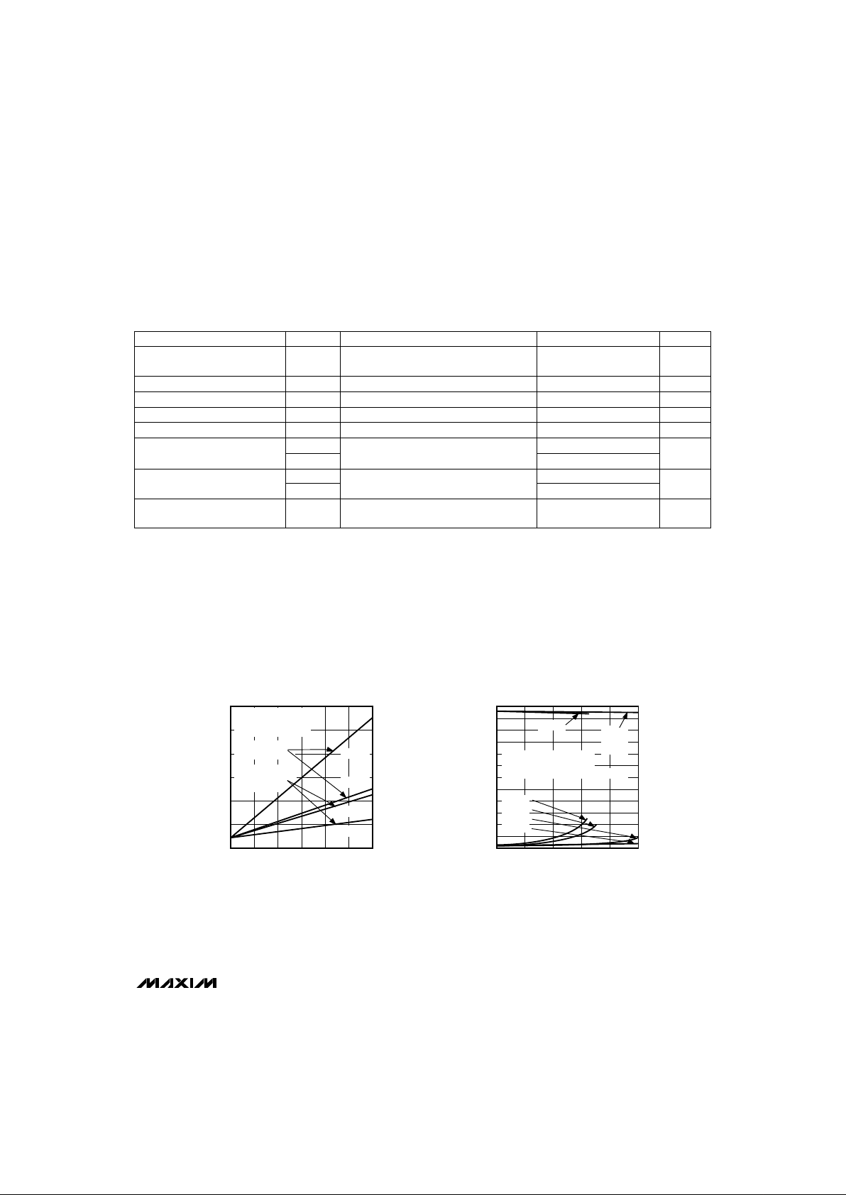
TIMING CHARACTERISTICS
(VCC= 3.0V to 3.6V, TA= T
MIN
to T
MAX
, unless otherwise noted.)
PARAMETER MIN TYP MAX UNITS
Transmitter Output Disable Time 600 ns
250 µs
Receiver Output Enable Time 70 200 ns
Receiver Output Disable Time 420 700 ns
CONDITIONS
Includes power-supply start-up
Receiver Propagation Delay
300 700
ns150pF load
800 2000
Transmitter Propagation Delay
800 2000
ns
2500pF 3kΩ load
300 700
SYMBOL
t
PLHR
t
PHLT
t
PLHT
t
DT
t
PHLR
t
ET
t
ER
t
DR
Transmitter Output Enable Time
4.0 10 30 V/µs
RL= 3kΩ to 7kΩ, CL= 50pF to 2500pF,
measured from +3V to -3V or -3V to +3V
Transition-Region Slew Rate
__________________________________________Typical Operating Characteristics
(VCC= 3.3V, TA = +25°C, unless otherwise noted.)
0204060
DATA RATE (kbps)
SUPPLY POWER (mW)
60
80
120
140
180
160
SUPPLY POWER vs.
DATA RATE
100
212 GR4
2500pF
1000pF
2500pF
80
ALL TRANSMITTERS
LOADED w/ 3kΩ AND
STATED CAPACITANCE
120
100
1000pF
3 TRANSMITTERS
AT DATA RATE
3 TRANSMITTERS,
1 AT DATA RATE,
1 LOW, 1 HIGH
0 50 100 150
DATA RATE (kbps)
OUTPUT VOLTAGE (V)
-6
-4
0
2
6
4
TRANSMITTER OUTPUT VOLTAGE vs.
DATA RATE
212 GR5
5000pF
4000pF
2500pF
1000pF
200
250
-2
4000pF
2500pF
1000pF
5000pF
ALL TRANSMITTERS
LOADED SIMULTANEOUSLY
w/ SPECIFIED CAPACITANCE AND 3kΩ
Data Rate 120 250 kbps
1000pF 3kΩ load on each transmitter,
150pF load on each receiver
 Loading...