

Page 1
19-0162; Rev 2; 2/94
EVALUATION KIT
INFORMATION INCLUDED
+3V-Powered, Low-Power,
True RS-232 Transceiver
________________General Description
The MAX212 RS-232 transceiver is intended for 3V-powered EIA/TIA-232E and V.28/V.24 communication interfaces where 3 drivers and 5 receivers are needed with
minimum power consumption. The operating voltage
range extends from 3.6V down to 3.0V while still maintaining true RS-232 and EIA/TIA-562 voltage levels.
A 1µA typical shutdown mode reduces power consumption, extending battery life in portable systems.
While shut down, all receivers can remain active or can
be disabled under logic control. This enables a system
incorporating the CMOS MAX212 to be in low-power
shutdown mode and monitor incoming RS-232 activity.
A guaranteed data rate of 120kbps provides compatibility with popular software for communicating with personal computers.
Three-state drivers on all receiver outputs are provided
so that multiple receivers, generally of different interface standards, can be wire-ORed at the UART.
The MAX212 is available in both small-outline (SO) and
shrink-small-outline (SSOP) packages. The SSOP
package occupies less than half of the board area
required by the equivalent SO package.
________________________Applications
Computers
Notebooks/Palmtops/Subnotebooks
Printers
Peripherals
Instruments
_______________Ordering Information
PART TEMP. RANGE PIN-PACKAGE
MAX212CWG 0°C to +70°C 24 Wide SO
MAX212CAG 0°C to +70°C 24 SSOP
MAX212C/D 0°C to +70°C Dice*
MAX212EWG -40°C to +85°C 24 Wide SO
MAX212EAG -40°C to +85°C 24 SSOP
* Dice are tested at TA= +25°C only.
____________________________Features
SUPERIOR TO BIPOLAR:
♦ Operates from Single +3.0V to +3.6V Supply
♦ 24-Pin SSOP or Wide SO Packages
♦ Meets All EIA/TIA-232E & EIA/TIA-562
Specifications
♦ 3mA Max Supply Current (Unloaded)
♦ 1µA Low-Power Shutdown Mode
♦ All Receivers Active During Low-Power Shutdown
♦ Mouse Compatible at 3.0V
♦ Low-Cost, Surface-Mount External Components
♦ 120kbps Guaranteed Data Rate—LapLink™
Compatible
♦ Three-State Receiver Outputs
♦ Evaluation Kit Available
♦ Flow-Through Pinout
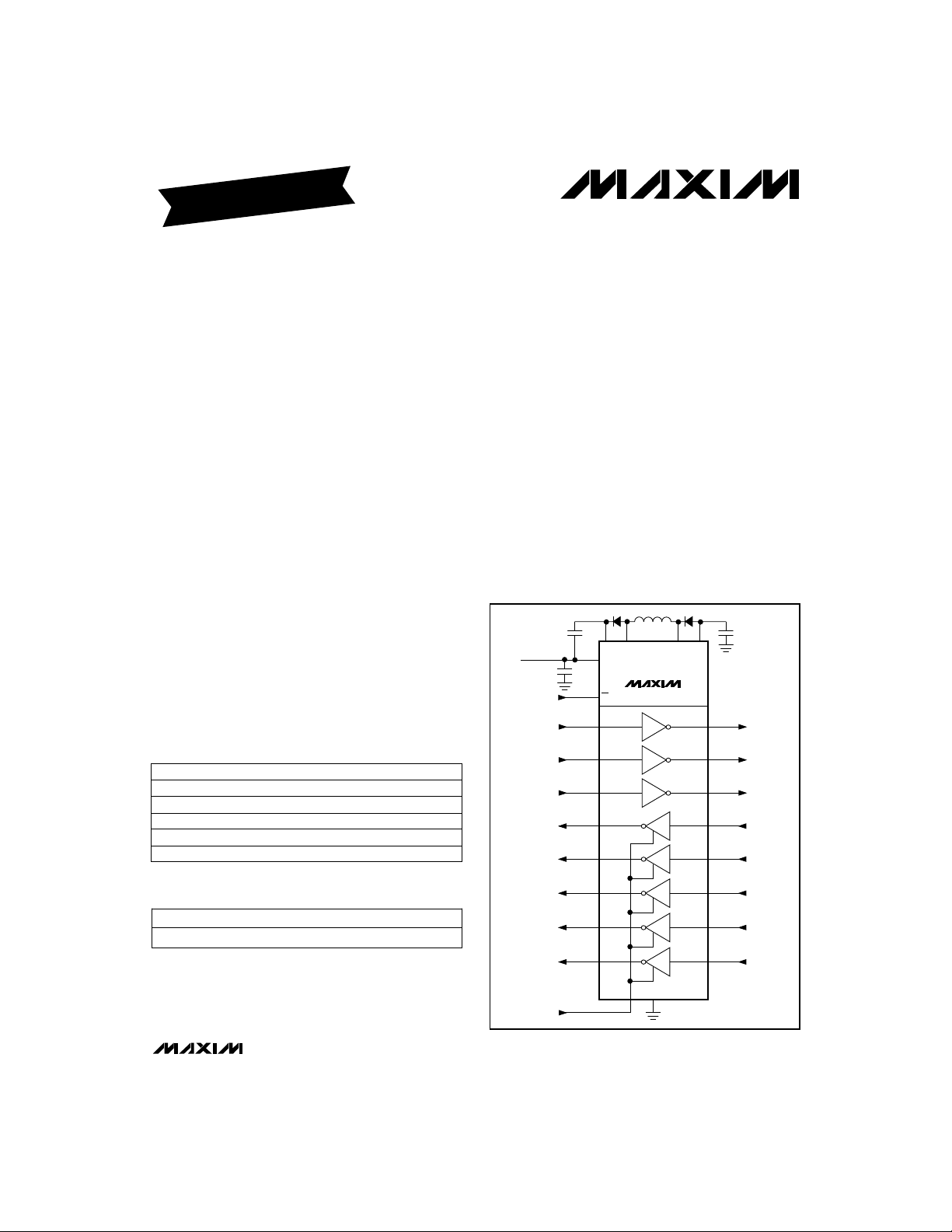
___________T ypical Operating Circuit
+3.3V
SHUTDOWN
1
LN
3
V
CC
DC-DC CONVERTER
4
SD
T1
11
IN
T2
12 16
IN
T3
13 15
IN
R1
622
OUT
R2
721
OUT
R3
820
OUT
MAX212
T1
T2
T3
21423
LP V-V+
T1
17
OUT
T2
OUT
T3
OUT
R1
IN
R1
R2
IN
R2
R3
IN
R3
MAX212
EV KIT TEMP. RANGE BOARD TYPE
R4
919
OUT
MAX212EVKIT-SSOP 0°C to +70°C Surface Mount
R5
10 18
OUT
EN
5
™LapLink is a registered trademark of Traveling Software.
ENABLE
________________________________________________________________
Call toll free 1-800-998-8800 for free samples or literature.
R4
IN
R4
R5
IN
R5
GND
24
Maxim Integrated Products
1
Page 2
+3V-Powered, Low-Power,
True RS-232 Transceiver
ABSOLUTE MAXIMUM RATINGS
Supply Voltages
.....................................................................-0.3V to +4.6V
V
CC
V+............................................................(V
V-........................................................................-7.4V to +2.0V
LN..............................................................-0.3V to (V+ + 1.0V)
LP.......................................................(V- - 1.0V) to (V+ + 0.3V)
Input Voltages
MAX212
, –S—D, EN..............................................-0.3V to (V+ + 0.3V)
T_
IN
...................................................................................±25V
R_
IN
Stresses beyond those listed under “Absolute Maximum Ratings” may cause permanent damage to the device. These are stress ratings only, and functional
operation of the device at these or any other conditions beyond those indicated in the operational sections of the specifications is not implied. Exposure to
absolute maximum rating conditions for extended periods may affect device reliability.
- 0.3V) to +7.4V
CC
Output Voltages
T_
................................................................................±15V
OUT
........................................................-0.3V to (V+ + 0.3V)
R_
OUT
Short-Circuit Duration, T_
Continuous Power Dissipation (T
Wide SO (derate 11.76mW/°C above +70°C)...............941mW
SSOP (derate 8.00mW/°C above +70°C) .....................640mW
Lead Temperature (soldering, 10sec).............................+300°C
.....................................Continuous
OUT
= +70°C)
A
ELECTRICAL CHARACTERISTICS
(VCC= 3.0V to 3.6V, TA= T
PARAMETER MIN TYP MAX UNITS
DC CHARACTERISTICS
Operating Voltage Range 3.0 3.6 V
VCCSupply Current 1.5 3.0 mA
Shutdown Supply Current 115µA
Shutdown Supply Current with
Receivers Active
LOGIC
Input Logic Threshold Low V
Input Logic Threshold High 2V
Input Current High 1 µA
Input Current Low 1 µA
Hysteresis 0.3 V
Logic Output Voltage Low 0.25 V
Logic Output Voltage High V
Logic Output Leakage Current ±10 µA
EIA/TIA-232E RECEIVERS
EIA/TIA-232E Input Voltage
Operating Range
EIA/TIA-232E Input Voltage
Threshold Low
EIA/TIA-232E Input Voltage
Threshold High
EIA/TIA-232E Input Hysteresis 0.7 V
EIA/TIA-232E Input Resistance 357kΩ
EIA/TIA-232E TRANSMITTERS
Output Voltage Swing (V
Output Resistance 300 Ω
EIA/TIA-232E Short-Circuit Current
MIN
HIGH
to T
, unless otherwise noted.)
MAX
Meets or exceeds EIA/TIA-232E specifications
No load, VCC= 3.3V
–S—
D= EN = GND, R_
–S—
D = GND, EN = V
T_IN, EN, –S—D; VCC= 3.0V to 3.6V
T_IN, EN, –S—D; VCC= 3.0V to 3.6V
T_IN, EN, –S—D; VIN= V
T_IN, EN, –S—D, VIN= GND
T_IN; V
I
OUT
I
OUT
EN = GND, 0V < R_
-15V < VIN< 15V
, V
All transmitters loaded 3kΩ to GND
)
LOW
VCC= V- = V+ = 0V, -2V < T_
= 3.3V
CC
= 1.0mA
= -1.0mA
CONDITIONS
= GND or V
IN
, R_IN= GND or V
CC
CC
< V
OUT
CC
OUT
CC
< 2V
CC
115µA
/ 3 V
CC
/ 3 V
CC
- 0.5 V
CC
-25 +25 V
0.4 V
2.8 V
±5.0 ±5.5 V
28 100 mA
2 _______________________________________________________________________________________
Page 3
+3V-Powered, Low-Power,
True RS-232 Transceiver
TIMING CHARACTERISTICS
(VCC= 3.0V to 3.6V, TA= T
PARAMETER MIN TYP MAX UNITS
Data Rate 120 250 kbps
Receiver Output Enable Time 70 200 ns
Receiver Output Disable Time 420 700 ns
Transmitter Output Enable Time
Transmitter Output Disable Time 600 ns
Receiver Propagation Delay
Transmitter Propagation Delay
Transition-Region Slew Rate
MIN
to T
, unless otherwise noted.)
MAX
SYMBOL
t
ER
t
DR
t
ET
t
DT
t
PHLR
t
PLHR
t
PHLT
t
PLHT
CONDITIONS
1000pF 3kΩ load on each transmitter,
150pF load on each receiver
Includes power-supply start-up
2500pF 3kΩ load
RL= 3kΩ to 7kΩ, CL= 50pF to 2500pF,
measured from +3V to -3V or -3V to +3V
250 µs
300 700
300 700
800 2000
800 2000
ns150pF load
ns
4.0 10 30 V/µs
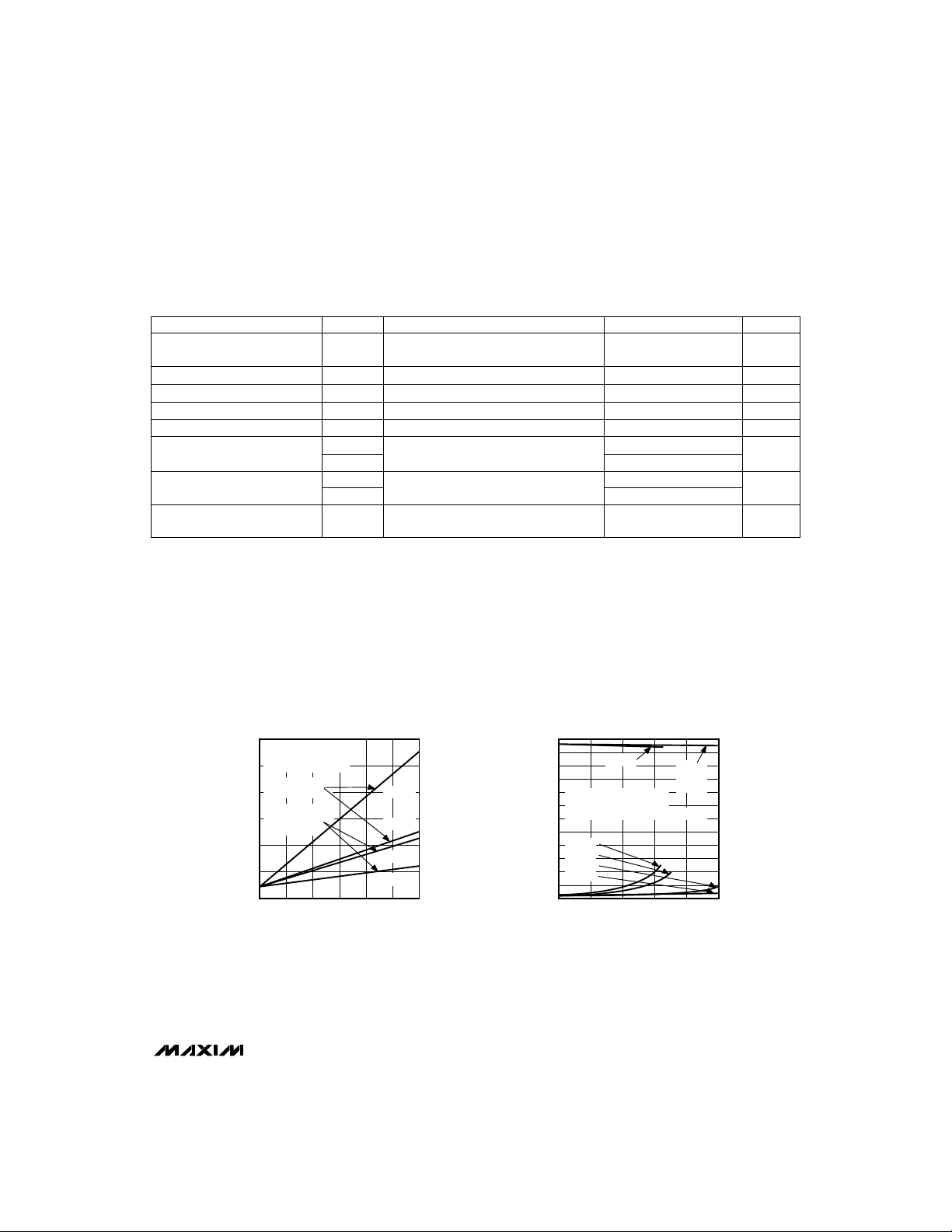
__________________________________________Typical Operating Characteristics
(VCC= 3.3V, TA = +25°C, unless otherwise noted.)
SUPPLY POWER vs.
180
ALL TRANSMITTERS
LOADED w/ 3kΩ AND
160
STATED CAPACITANCE
3 TRANSMITTERS
140
AT DATA RATE
3 TRANSMITTERS,
120
1 AT DATA RATE,
1 LOW, 1 HIGH
100
SUPPLY POWER (mW)
80
60
0204060
DATA RATE
DATA RATE (kbps)
212 GR4
2500pF
1000pF
2500pF
1000pF
120
100
80
TRANSMITTER OUTPUT VOLTAGE vs.
DATA RATE
6
4
2
0
-2
OUTPUT VOLTAGE (V)
-4
-6
0 50 100 150
5000pF
ALL TRANSMITTERS
LOADED SIMULTANEOUSLY
w/ SPECIFIED CAPACITANCE AND 3kΩ
5000pF
4000pF
2500pF
1000pF
DATA RATE (kbps)
4000pF
2500pF
1000pF
200
212 GR5
250
MAX212
_______________________________________________________________________________________ 3
Page 4

+3V-Powered, Low-Power,
True RS-232 Transceiver
____________________________Typical Operating Characteristics (continued)
(VCC= 3.3V, TA = +25°C, unless otherwise noted.)
SUPPLY POWER vs.
180
MAX212
160
140
120
SUPPLY POWER (mW)
100
80
2.5 3.0 3.5 4.0
SUPPLY VOLTAGE
ALL TRANSMITTERS
AT SPECIFIED DATA RATES
w/ 2500pF AND 3kΩ LOADS
SUPPLY VOLTAGE (V)
120kbps
64kbps
20kbps
212 GR2
4.5
80
70
60
50
40
SUPPLY CURRENT (mA)
30
20
0 1000 2000 3000
_____________________Pin Description
PIN
6-10
11-13
15-17
18-22
NAME FUNCTION
1
2
3
LN
LP
V
CC
Inductor/Diode Connection Point
Inductor/Diode Connection Point
Supply Voltage Input, 3.0V to 3.6V
Shutdown Control. Connect to V
4
–S—
D
for normal operation. Connect to
GND to shut down the power supply
and to disable the drivers. Receiver
status is not changed by this control.
Receiver Enable Control. Connect
5
EN
to VCCfor normal operation.
Connect to GND to force the
receiver outputs into a high-Z state.
R1
-
OUT
R5
OUT
T1IN-T3
V-14
T3
OUT
T1
OUT
R5IN-R1
Receiver Outputs, swing GND
to V
Transmitter Inputs
IN
Negative Supply generated on-board
Transmitter Outputs
Receiver Inputs
IN
V+ Positive Supply generated on-board23
GND Ground24
CC
SUPPLY CURRENT vs.
LOAD CAPACITANCE
ALL TRANSMITTERS
AT SPECIFIED CAPACITANCE AND
DATA RATES w/ 3kΩ LOADS
LOAD CAPACITANCE (pF)
_______________Detailed Description
The MAX212 line driver/receiver is intended for 3Vpowered EIA/TIA-232E and V.28/V.24 communications
interfaces where 3 drivers and 5 receivers are
required. The operating voltage range extends from
3.6V down to 3.0V while still maintaining true RS-232
and EIA/TIA-562 transmitter output voltage levels.
CC
The circuit comprises three sections: power supply,
transmitters, and receivers. The power-supply section converts the supplied 3V to about ±6.5V, to provide the voltages necessary for the drivers to meet
true RS-232 levels. External components are small
and inexpensive.
The transmitters and receivers are guaranteed to operate at data rates of 120kbps.
A shutdown mode reduces current to 1µA to extend
battery life in portable systems. While shut down, all
receivers can remain active or can be disabled under
logic control. This enables a system incorporating the
MAX212 to be in low-power shutdown mode and still
monitor incoming RS-232 activity.
Three-state drivers on all receiver outputs are provided
so that multiple receivers, generally of different interface standards, can be wire-ORed at the UART.
120kbps
64kbps
20kbps
4000
5000
14
212 GR3
13
12
11
10
9
SLEW RATE (V/µs)
ALL TRANSMITTERS
8
LOADED SIMULTANEOUSLY
w/ SPECIFIED CAPACITANCE AND 3kΩ
7
6
500 1500 2500 3500
SLEW RATE vs.
LOAD CAPACITANCE
RISING EDGE
FALLING EDGE
LOAD CAPACITANCE (pF)
4500
212 GR6
4 _______________________________________________________________________________________
Page 5

+3V-Powered, Low-Power,
True RS-232 Transceiver
D1
1N6050
15µH
0.33µF
SHUTDOWN
ENABLE
0.68µF
+3.3V
C3
C1
1
LN
3
V
CC
+3.3V TO ±6.5V
DC-DC CONVERTER
4
11
12 16
13 15
622
721
820
919
10 18
MAX212
SD
T1
IN
T2
IN
T3
IN
R1
OUT
R2
OUT
R3
OUT
R4
OUT
R5
OUT
EN
GND
24
5
Figure 1. Typical Application Circuit
L
D2
1N6050
C2
21423
LP V-V+
0.33µF
The switch-mode power supply uses a single inductor
with two inexpensive diodes and two capacitors to
generate ±6.5V from the 3.0V to 3.6V input. Figure 1
shows the complete circuit for the power supply.
Use a 15µH inductor with a saturation current rating of at
Switch-Mode Power Supply
MAX212
least 350mA and under 1Ω resistance. Sample surfacemount inductors are available from Maxim. Use 1N6050
diodes or equivalent. Surface-mount equivalents for the
1N6050 include the Motorola MMBD6050LT1, Philips
PMBD6050, and Allegro (formerly Sprague) TMPD6050LT.
T1
17
T1
T2
T3
OUT
T2
OUT
T3
OUT
R1
R1
R2
R3
R4
R5
IN
R2
IN
R3
IN
R4
IN
R5
IN
For C1 and C2, use ceramic capacitors with values no
less than indicated in Figure 1. These capacitors determine the ripple on V+ and V-, but not the absolute voltages. Bypass VCCto GND with at least 0.33µF close to
the MAX212. Increase this to 4.7µF if there are no other
VCCsupply bypass components less than 6 inches
(15cm) away from the MAX212.
Component suppliers are listed in Table 1.
RS-232 Drivers
All three drivers are identical and deliver EIA/TIA-232E
and EIA/TIA-562 output voltage levels when VCCis
between 3.0V and 3.6V. Disable the drivers by taking
the –S—Dpin to GND. The transmitter outputs are forced
into a high-impedance state when –S—D is grounded.
RS-232 Receivers
All five receivers are identical and accept
EIA/TIA-232E and EIA/TIA-562 input signals. The CMOS
receiver outputs swing rail-to-rail (0V to VCC). When EN
is high, the receivers are active regardless of –S—D’s status.
When EN is low, the receivers’ outputs are put into a
high-impedance state. This allows two RS-232 ports (or
two parts of different types) to be wire-ORed at the UART.
Table 1. Suggested Component Suppliers
MANUFACTURER PART NUMBER PHONE NUMBER FAX NUMBER
Allegro TMPD6050LT USA (508) 853-5049
Motorola MMBD6050LT1 USA (408) 991-7420
Murata LQH4N150K-TA
Philips PMBD6050 USA (401) 762-3800 USA (401) 767-4493
Sumida CD43150
TDK NLC453232T-150K
_______________________________________________________________________________________ 5
USA (508) 853-5000
USA (408) 749-0510
USA (404) 831-9172
Japan (075) 951-9111
USA (708) 956-0666
Japan (03) 3607-5111
USA (708) 803-6100
Japan (03) 3278-5111
USA (404) 436-3030
Japan (075) 955-6526
USA (708) 956-0702
Japan (03) 3607-5428
USA (708) 803-6296
Japan (03) 3278-5358
Page 6

+3V-Powered, Low-Power,
True RS-232 Transceiver
–S—
D and EN determine the operation of the MAX212
Operating Modes
as follows:
–S—
D
L L High-Z High-Z Off Minimum
MAX212
L H Enabled High-Z Off Minimum
H L High-Z Enabled On Normal
H H Enabled Enabled On Normal
EN
RECEIVER
OUTPUTS
DRIVER
OUTPUTS
DC-DC
CONVERTER
SUPPLY
CURRENT
Shutdown
V+ and V- are disabled and the transmitters are put into
a high-impedance state when –S—Dis taken to logic low.
Receiver operation is not affected, but power consumption is dramatically reduced while in shutdown mode.
Supply current is minimized when the receiver inputs are
static in any of three states: floating (ground), less than
GND, or greater than VCC. This will be true for all static
RS-232 conditions. The presence of AC signals on receiver inputs will increase VCCcurrent in shutdown.
From a low-power system perspective, powering-up with
non-critical or unused sections of circuitry shut down or
deselected is generally recommended. Activating these
sections only when required saves power and reduces
power-up current surges. Powering-up the MAX212 in
shutdown mode (holding the shutdown pin,
–S—
D, low until VCC> 2.7V), helps to achieve this.
Driving the MAX212 from 5V Logic
The MAX212 can interface with 5V logic while it operates
from a 3V supply, however a 200kΩseries resistor between
–S—
D and the +5V logic signal is required (see Figure 2).
This protects the MAX212 by preventing –S—Dfrom sinking
current while V+ is powering up. Also, the UART must not
be permitted to send a logic high to the MAX212’s EN or
transmitter input pins until –S—Dis high (not shut down).
LN
200k
V+
DC-DC CONVERTER
SD
T_
IN
R_
OUT
+3.3V
+5V
LOGIC
SIGNALS
Figure 2. Connecting to +5V Logic
MAX212
EN
LP V-
T
X
X3
R
X
X5
GND
T_
OUT
R_
IN
Mouse Driveability
The MAX212 has been specifically designed to power
serial mice while operating from low-voltage power
supplies. It has been tested with samples of ten major
mouse models from six manufacturers, including the
leading three, Logitech (5 models), Mouse Systems,
and Microsoft. The MAX212 successfully drove all serial mice and met their respective current and voltage
requirements (Figure 1).
Figure 3 shows the transmitter output voltages under
increasing load current. The MAX212’s switching regulator ensures the transmitters will supply at least ±5V
during worst-case load conditions.
EIA/TIA-232E and 562 Standards
Most of the power drawn by RS-232 circuits is consumed because the EIA/TIA-232E standard demands
that at least ±5V be delivered by the transmitters to
impedances that can be as low as 3kΩ. For applica-
____________________________+3V Powered RS-232 Transceivers from Maxim
PART
MAX212 3.0 to 3.6 3/5 5 250 True RS-232 from +3V
MAX560 3.0 to 3.6 4/5 2 120 2 receivers active in shutdown
MAX561 3.0 to 3.6 4/5 0 120 Pin compatible with MAX241
MAX562 2.7 to 5.25 3/5 5 250 Wide supply range
6 _______________________________________________________________________________________
POWER-SUPPLY
VOLTAGE
(V)
No. OF
TRANSMITTERS/
RECEIVERS
No. OF
RECEIVERS
ACTIVE IN
SHUTDOWN
DATA RATE
(kbps)
FEATURES
Page 7

+3V-Powered, Low-Power,
True RS-232 Transceiver
TRANSMITTER OUTPUT VOLTAGE vs.
LOAD CURRENT PER TRANSMITTER
6
T1
AND T2
OUT
IN
, T1
= GND,
OUT
OUT
T3
OUT
5 6
4
T1IN AND T2
2
= VCC = 3.0V,
T3
IN
, T2
T3
OUT
OUT
ALL LOADED
0
SIMULTANEOUSLY
-2
-4
TRANSMITTER OUTPUT VOLTAGE (V)
-6
1234
LOAD CURRENT PER TRANSMITTER (mA)
Figure 3. Mouse Emulation Circuit Current
212 GR1
tions where power consumption is especially critical,
the EIA/TIA-562 standard provides an alternative.
EIA/TIA-562 transmitter output voltage levels need only
reach ±3.7V, and because they need only drive the
same 3kΩ receiver loads specified by RS-232, total
power consumption is considerably reduced. Since the
EIA/TIA-232E and EIA/TIA-562 receiver input voltage
thresholds are the same, interoperability between the two
standards is guaranteed and devices from both standards will communicate with each other successfully.
Maxim’s MAX560 and MAX561 are EIA/TIA-562 transceivers that operate on a single supply from 3.0V to
3.6V, and the MAX562 transceiver operates from 2.7V
to 5.25V while producing EIA/TIA-562 levels.
______________________Evaluation Kit
The MAX212 evaluation kit (EV kit) is a fully assembled and tested, surface-mount demonstration board
that provides quick and easy evaluation of the
MAX212.
The MAX212 EV kit is intended for 3.3V ±300mV-powered EIA/TIA-232E and V.28/V.24 communications
interfaces where 3 drivers and 5 receivers are needed
with minimum power consumption.
A logic or pin-selectable shutdown mode reduces
current to 1µA. While shut down, all receivers can
remain active or can be disabled under logic control
via the EN input.
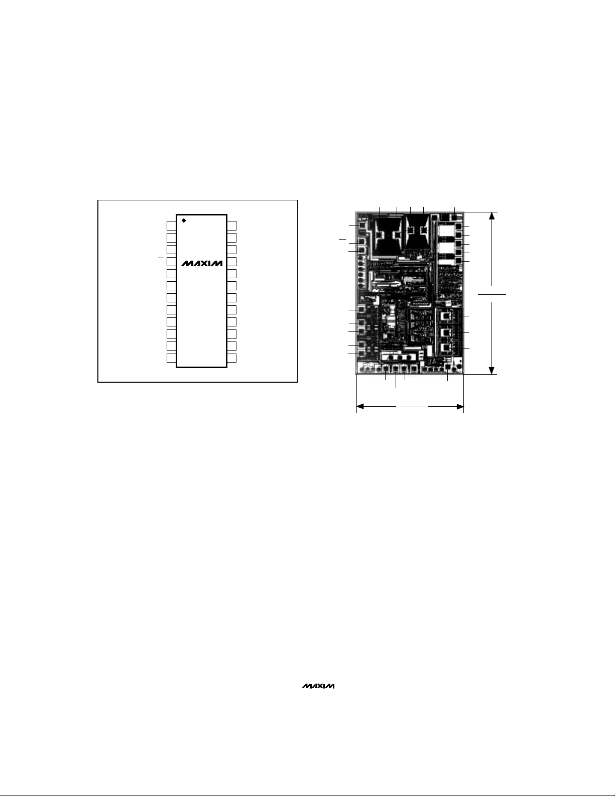
MAX212
Figure 4. MAX212 Evaluation Kit
_______________________________________________________________________________________ 7
Page 8
+3V-Powered, Low-Power,
True RS-232 Transceiver
_________________Pin Configuration
TOP VIEW
MAX212
LN
LP
V
CC
SD
EN
R1
OUT
R2
OUT
R3
OUT
R4
OUT
R5
OUT
T1
IN
T2
IN
1
2
3
4
MAX212
5
6
7
8
9
10
11
12
SSOP/WIDE SO
GND
24
V+
23
R1
22
IN
R2
21
IN
R3
20
IN
R4
19
IN
R5
18
IN
T1
17
OUT
T2
16
OUT
T3
15
OUT
V-
14
T3
13
IN
___________________Chip Topography
LP GND
IN
T2
T3
IN
IN
0.1"
(2.54mm)
GNDLN
V+
R1
IN
R2
IN
R3
IN
R4
IN
R5
IN
0.15"
(3.81mm)
T1
OUT
T2
OUT
T3
OUT
V-
V
CC
V
CC
SD
EN
R1
OUT
R2
OUT
R3
OUT
R4
OUT
R5
OUT
T1
TRANSISTOR COUNT: 1382 ;
SUBSTRATE CONNECTED TO V+.
Maxim cannot assume responsibility for use of any circuitry other than circuitry entirely embodied in a Maxim product. No circuit patent licenses are
implied. Maxim reserves the right to change the circuitry and specifications without notice at any time.
8
___________________Maxim Integrated Products, 120 San Gabriel Drive, Sunnyvale, CA 94086 (408) 737-7600
© 1993 Maxim Integrated Products Printed USA is a registered trademark of Maxim Integrated Products.
 Loading...