

General Description
The MAX2112 low-cost, direct-conversion tuner IC is
designed for satellite set-top and VSAT applications.
The IC is intended for 8PSK and Digital Video
Broadcast (DVB-S2) applications.
The MAX2112 directly converts the satellite signals
from the LNB to baseband using a broadband I/Q
downconverter. The operating frequency range extends
from 925MHz to 2175MHz.
The device includes an LNA and an RF variable-gain
amplifier, I and Q downconverting mixers, and baseband
lowpass filters with programmable cutoff frequency control
and digitally controlled baseband variable-gain amplifiers.
Together, the RF and baseband variable-gain amplifiers
provide more than 80dB of gain control range. The IC is
compatible with virtually all DVB-S2 demodulators.
The MAX2112 includes fully monolithic VCOs, as well as
a complete fractional-N frequency synthesizer.
Additionally, an on-chip crystal oscillator is provided
along with a buffered output for driving additional tuners
and demodulators. Synthesizer programming and device
configuration are accomplished with a 2-wire serial interface. The IC features a VCO autoselect (VAS) function
that automatically selects the proper VCO. For multituner
applications, the device can be configured to have one
of two 2-wire interface addresses. A low-power standby
mode is available whereupon the signal path is shut
down while leaving the reference oscillator, digital interface, and buffer circuits active, providing a method to
reduce power in single and multituner applications.
The MAX2112 is the most advanced DBS tuner available today. The low noise figure eliminates the need for
an external LNA. A small number of passive components are needed to form a complete DVB-S2 RF frontend solution. The tuner is available in a very small
28-pin thin QFN package.
Applications
DirecTV and Dish Network DBS
DVB-S2
VSATs
Features
o 925MHz to 2175MHz Frequency Range
o Monolithic VCO
Low Phase Noise: -97dBc/Hz at 10kHz
No Calibration Required
o High Dynamic Range: -75dBm to 0dBm
o Integrated Variable BW LP Filters: 4MHz to 40MHz
o Single +3.3V ±5% Supply
o Low-Power Standby Mode
o Address Pin for Multituner Applications
o Differential I/Q Interface
o I2C 2-Wire Serial Interface
o Very Small 28-Pin TQFN Package
MAX2112
Complete, Direct-Conversion
Tuner for DVB-S2 Applications
________________________________________________________________
Maxim Integrated Products
1
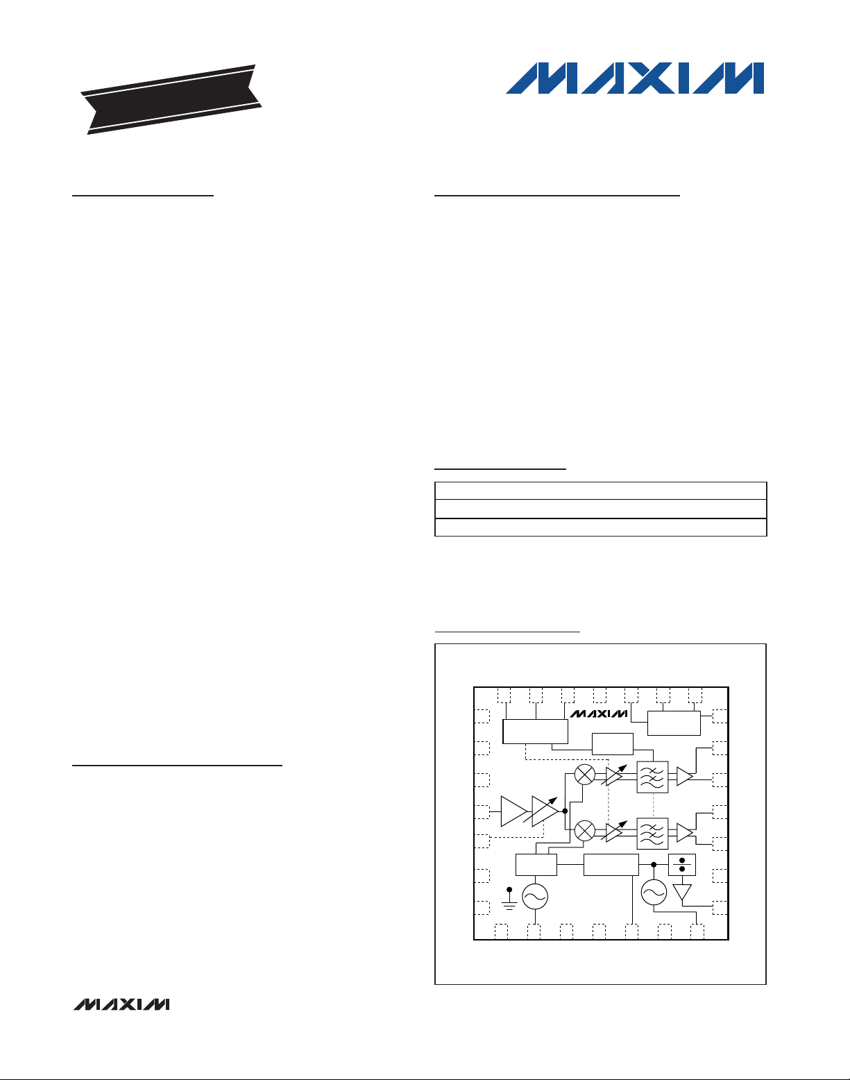
Pin Configuration/
Functional Diagram
Ordering Information
19-0869; Rev 2; 5/10
For pricing, delivery, and ordering information, please contact Maxim Direct at 1-888-629-4642,
or visit Maxim’s website at www.maxim-ic.com.
*
EP = Exposed paddle.
+
Denotes a lead(Pb)-free/RoHS-compliant package.
EVALUATION KIT
AVAILABLE
PART TEMP RANGE PIN-PACKAGE
MAX2112CTI+ 0°C to +70°C
28 Thin QFN-EP*
MAX2112ETI+ -40°C to +85°C
28 Thin QFN-EP*
VCC_RF2
VCC_RF1
GND
RFIN
GC1
VCC_LO
+
1
2
3
4
5
6
ADDR
27
28
INTERFACE LOGIC
AND CONTROL
DIV2/DIV4
EP
SCL
VCC_BB
25
LPF BW
CONTROL
QDC-
DC OFFSET
CORRECTION
SDA
26 24 23
MAX2112
FREQUENCY
SYNTHESIZER
QDC+
IDC-
21
20
19
18
17
16
IDC+
IOUT-
IOUT+
QOUT-
QOUT+
VCC_DIG
VCC_VCO
XTAL
15
REFOUT
7
10 12
8
VCOBYP
9
VTUNE
11 132214
CPOUT
GNDSYN
GNDTUNE
VCC_SYN
MAX2112
Complete, Direct-Conversion
Tuner for DVB-S2 Applications
2 _______________________________________________________________________________________
ABSOLUTE MAXIMUM RATINGS
DC ELECTRICAL CHARACTERISTICS
(MAX2112 Evaluation Kit: V
CC
= +3.13V to +3.47V, TA= 0°C to +70°C (MAX2112CTI+), TA= -40°C to +85°C (MAX2112ETI+), V
GC1
= +0.5V (max gain), default register settings except BBG[3:0] = 1011. No input signals at RF, baseband I/Os are open circuited.
Typical values measured at V
CC
= +3.3V, TA= +25°C.) (Note 1)
Stresses beyond those listed under “Absolute Maximum Ratings” may cause permanent damage to the device. These are stress ratings only, and functional
operation of the device at these or any other conditions beyond those indicated in the operational sections of the specifications is not implied. Exposure to
absolute maximum rating conditions for extended periods may affect device reliability.
VCCto GND...........................................................-0.3V to +3.9V
All Other Pins to GND.................................-0.3V to (V
CC
+ 0.3V)
RF Input Power: RFIN .....................................................+10dBm
VCOBYP, CPOUT, XTAL, REFOUT, IOUT_, QOUT_ , IDC_,
QDC_ to GND Short-Circuit Protection...............................10s
Continuous Power Dissipation (T
A
= +70°C)
28-Pin Thin QFN (derated 34.5mW/°C above +70°C) ...2.75W
Operating Temperature Range (MAX2112CTI+) ......0°C to +70°C
Operating Temperature Range (MAX2112ETI+) ...-40°C to +85°C
Junction Temperature......................................................+150°C
Storage Temperature Range .............................-65°C to +160°C
Lead Temperature (soldering, 10s) .................................+300°C
Soldering Temperature (reflow) .......................................+260°C
CAUTION! ESD SENSITIVE DEVICE
PARAMETER CONDITIONS MIN TYP MAX UNITS
SUPPLY
Supply Voltage 3.13 3.3 3.47 V
Supply Current
ADDRESS SELECT INPUT (ADDR)
Digital Input Voltage High, V
Digital Input Voltage Low, V
Digital Input Current High, I
Digital Input Current Low, I
ANALOG GAIN-CONTROL INPUT (GC1)
Input Voltage Range Maximum gain = 0.5V 0.5 2.7 V
Input Bias Current -50 +50 µA
VCO TUNING VOLTAGE INPUT (VTUNE)
Input Voltage Range 0.4 2.3 V
2-WIRE SERIAL INPUTS (SCL, SDA)
Clock Frequency 400 kHz
Input Logic-Level High
Input Logic-Level Low
Input Leakage Current Digital inputs = GND or V
2-WIRE SERIAL OUTPUT (SDA)
Output Logic-Level Low I
Receive mode, bit STBY = 0 100 160
Standby mode, bit STBY = 1 3
IH
IL
IH
IL
= 1mA 0.4 V
SINK
2.4 V
-50 µA
0.7 x
V
CC
CC
±0.1 ±1 µA
0.5 V
50 µA
0.3 x
V
CC
mA
V
V
MAX2112
Complete, Direct-Conversion
Tuner for DVB-S2 Applications
_______________________________________________________________________________________ 3
AC ELECTRICAL CHARACTERISTICS
(MAX2112 Evaluation Kit: V
CC
= +3.13V to +3.47V, TA= 0°C to +70°C (MAX2112CTI+), TA= -40°C to +85°C (MAX2112ETI+), default
register settings except BBG[3:0] = 1011. Typical values measured at V
CC
= +3.3V, TA= +25°C.) (Note 1)
PARAMETER CONDITIONS MIN TYP MAX UNITS
MAIN SIGNAL PATH PERFORMANCE
Input Frequency Range (Note 2) 925 2175 MHz
RF Gain-Control Range (GC1) 0.5V < V
Baseband Gain-Control Range Bits GC2 = 1111 to 0000 13 15 dB
In-Band Input IP3 (Note 3) +2 dBm
Out-of-Band Input IP3 (Note 4) +15 dBm
Input IP2 (Note 5) +40 dBm
Adjacent Channel Protection (Note 6) 25 dB
Noise Figure
Minimum RF Input Return Loss 925MHz < f
BASEBAND OUTPUT CHARACTERISTICS
Nominal Output Voltage Swing R
I/Q Amplitude Imbalance Measured at 500kHz; filter set to 22.27MHz ±1 dB
I/Q Quadrature Phase Imbalance Measured at 500kHz; filter set to 22.27MHz 3.5 D eg r ees
S i ng l e- E nd ed I/Q Outp ut Im p ed ance Real ZO, from 1MHz to 40MHz 30 Ω
Output 1dB Compression Voltage Differential 3 V
Baseband Highpass -3dB
Frequency Corner
BASEBAND LOWPASS FILTERS
Filter Bandwidth Range 4 40 MHz
Rejection Ratio At 2 x f
Group Delay Up to 1dB bandwidth 37 ns
Ratio of In-Filter-Band to Out-ofFilter-Band Noise
FREQUENCY SYNTHESIZER
RF-Divider Frequency Range 925 2175 MHz
RF-Divider Range (N) 19 251
Refer ence- D i vi d er Fr eq uency Rang e 12 30 MHz
Reference-Divider Range (R) 1 1
Phase-Detector Comparison
Frequency
VOLTAGE-CONTROLLED OSCILLATOR AND LO GENERATION
Guaranteed LO Frequency Range 925 2175 MHz
< 2.7V 65 73 dB
GC1
V
is set to 0.5V (maximum RF gain) and BBG[3:0] is
GC1
adjusted to give a 1V
-75dBm CW input tone at 1500MHz
Starting with the same BBG[3:0] setting as above, V
is adjusted to back off RF gain by 10dB (Note 7)
< 2175MHz, in 75Ω system 12 dB
RF
= 2kΩ//10pF 0.5 1 V
LOAD
47nF capacitors at IDC_, QDC_ 400 Hz
-3dB
f
112.5MHz
f
f
f
= 100Hz to 22.5MHz, f
INBAND
= 10kHz -97
OFFSET
= 100kHz -100LO Phase Noise
OFFSET
= 1MHz -122
OFFSET
baseband output level for a
P-P
GC1
OUTBAND
= 87.5MHz to
8
912
39 dB
25 dB
12 30 MHz
dB
P-P
P-P
dBc/Hz
MAX2112
Complete, Direct-Conversion
Tuner for DVB-S2 Applications
4 _______________________________________________________________________________________
AC ELECTRICAL CHARACTERISTICS (continued)
(MAX2112 Evaluation Kit: V
CC
= +3.13V to +3.47V, TA= 0°C to +70°C (MAX2112CTI+), TA= -40°C to +85°C (MAX2112ETI+), default
register settings except BBG[3:0] = 1011. Typical values measured at V
CC
= +3.3V, TA= +25°C.) (Note 1)
Note 1: MAX2112CTI+: Min/max values are production tested at TA= +70°C. Min/max limits at TA= 0°C and TA= +25°C are
guaranteed by design and characterization.
MAX2112ETI+: Min/max values are production tested at T
A
= +85°C. Min/max limits at TA= -40°C and TA= +25°C are
guaranteed by design and characterization.
Note 2: Input gain range specifications met over this band.
Note 3: In-band IIP3 test conditions: GC1 set to provide the nominal baseband output drive when mixing down a -23dBm tone at
2175MHz to 5MHz baseband (f
LO
= 2170MHz). Baseband gain is set to its default value (BBG[3:0] = 1011). Two tones at
-26dBm each are applied at 2174MHz and 2175MHz. The IM3 tone at 3MHz is measured at baseband, but is referred to the
RF input.
Note 4: Out-of-band IIP3 test conditions: GC1 set to provide nominal baseband output drive when mixing down a -23dBm tone at
2175MHz to 5MHz baseband (f
LO
= 2170MHz). Baseband gain is set to its default value (BBG[3:0] = 1011). Two tones at
-20dBm each are applied at 2070MHz and 1975MHz. The IM3 tone at 5MHz is measured at baseband, but is referred to the
RF input.
Note 5: Input IP2 test conditions: GC1 set to provide nominal baseband output drive when mixing down a -23dBm tone at 2175MHz
to 5MHz baseband (f
LO
= 2170MHz). Baseband gain is set to its default value (BBG[3:0] = 1011). Two tones at -20dBm
each are applied at 925MHz and 1250MHz. The IM2 tone at 5MHz is measured at baseband, but is referred to the RF input.
Note 6: Adjacent channel protection test conditions: GC1 is set to provide the nominal baseband output drive with a 2110MHz
27.5Mbaud signal at -55dBm. GC2 set for mid-scale. The test signal shall be set for PR = 7/8 and SNR of -8.5dB. An adjacent channel at ±40MHz is added at -25dBm. DVB-S BER performance of 2E-4 shall be maintained for the desired signal.
GC2 may be adjusted for best performance.
Note 7: Guaranteed by design and characterization at T
A
= +25°C.
Note 8: See Table 16 for crystal ESR requirements.
PARAMETER CONDITIONS MIN TYP MAX UNITS
XTAL/REFERENCE OSCILLATOR INPUT AND OUTPUT BUFFER
XTAL Oscillator Frequency Range Parallel-resonance-mode crystal (Note 8) 12 30 MHz
Input Overdrive level AC-coupled sine-wave input 0.5 1 2.0 V
XTAL Output-Buffer Divider Range 1 8
XTAL Output Voltage Swing 4MHz to 30MHz, C
XTAL Output Duty Cycle 50 %
= 10pF 1 1.5 2 V
LOAD
P-P
P-P
MAX2112
Complete, Direct-Conversion
Tuner for DVB-S2 Applications
_______________________________________________________________________________________
5
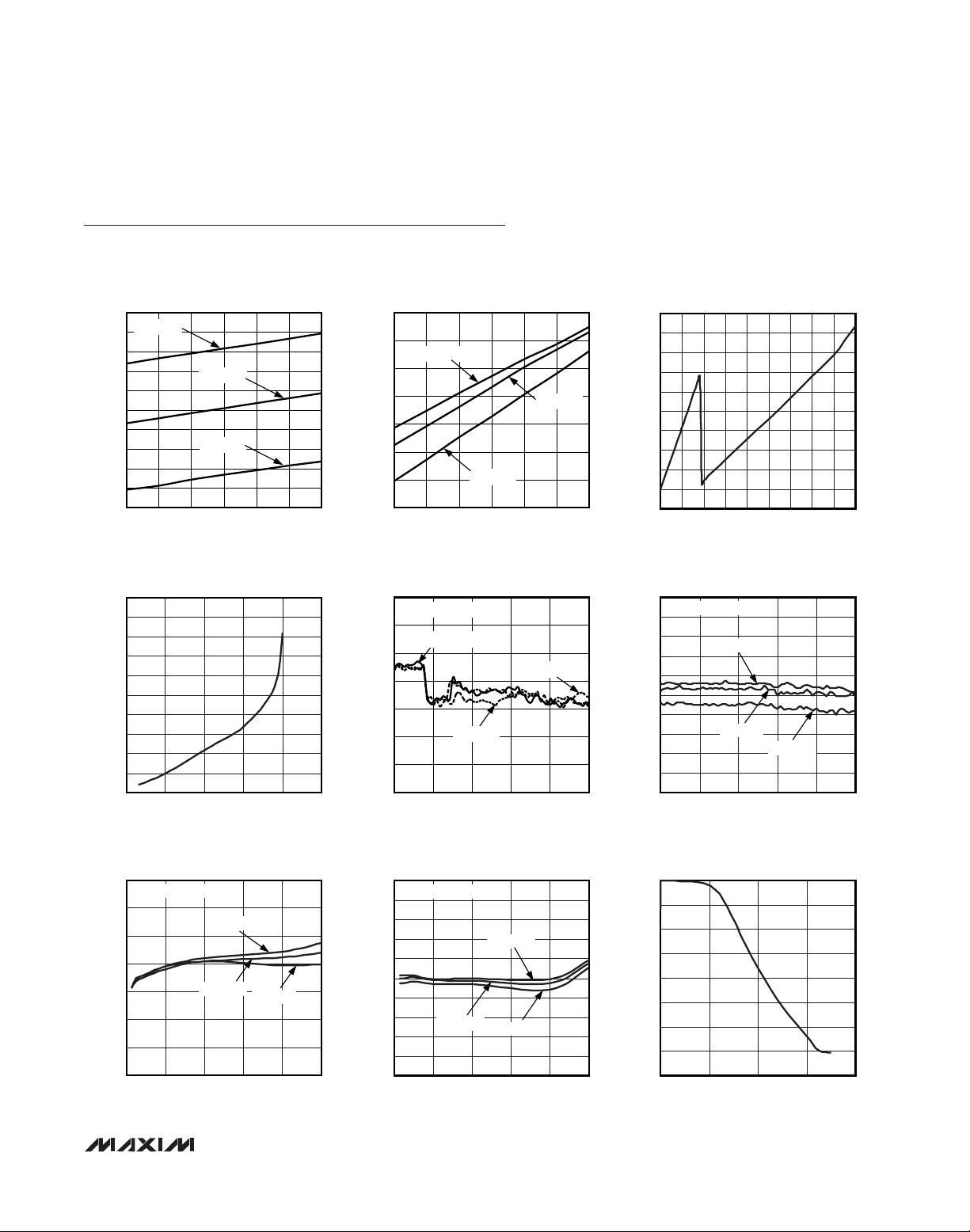
Typical Operating Characteristics
(MAX2112 Evaluation Kit: V
CC
= +3.3V, TA= +25°C, baseband output frequency = 5MHz; V
GC1
= +1.2V, default register settings
except BBG[3:0] = 1011.)
STANDBY MODE SUPPLY CURRENT
SUPPLY CURRENT vs. SUPPLY VOLTAGE
98
TA = +85°C
97
96
95
94
93
92
91
SUPPLY CURRENT (mA)
90
89
88
3.0 3.6
-10
-15
-20
-25
-30
-35
-40
-45
-50
BASEBAND 3RD-ORDER HARMONIC (dBc)
-55
-60
1.0 3.5
TA = +25°C
TA = -40°C
SUPPLY VOLTAGE (V)
HD3 vs. V
OUT
V
(V
)
OUT
P-P
QUADRATURE PHASE
3.53.43.33.23.1
3.02.52.01.5
3.0
2.9
MAX2112 toc01
2.8
2.7
2.6
2.5
SUPPLY CURRENT (mA)
2.4
2.3
93.5
92.5
MAX2112 toc04
91.5
90.5
89.5
88.5
QUADRATURE PHASE (°)
87.5
86.5
3.0 3.1 3.2 3.3 3.4 3.5 3.6
QUADRATURE PHASE vs. LO FREQUENCY
f
BASEBAND
900 1200 1500 1800 2100 2400
QUADRATURE MAGNITUDE MATCHING
vs. BASEBAND FREQUENCY
93.5
fLO = 925MHz
92.5
91.5
90.5
89.5
QUADRATURE PHASE (°)
88.5
87.5
86.5
020
BASEBAND FREQUENCY (MHz)
TA = +85°C
TA = +25°C
TA = -40°C
161284
1.0
fLO = 925MHz
0.8
MAX2112 toc06a
0.6
0.4
0.2
0
-0.2
-0.4
-0.6
-0.8
QUADRATURE MAGNITUDE MATCHING (dB)
-1.0
020
vs. SUPPLY VOLTAGE
TA = +85°C
TA = +25°C
TA = -40°C
SUPPLY VOLTAGE (V)
= 10MHz
TA = +25°C
TA = +85°C
TA = -40°C
LO FREQUENCY (MHz)
vs. BASEBAND FREQUENCY
TA = +85°C
TA = +25°C
BASEBAND FREQUENCY (MHz)
TA = -40°C
vs. BASEBAND FILTER CUTOFF FREQUENCY
104
102
MAX2112 toc02
100
98
96
94
92
90
SUPPLY CURRENT (mA)
88
86
84
440
QUADRATURE MAGNITUDE MATCHING
1.0
0.8
MAX2112 toc05a
0.6
0.4
0.2
0
-0.2
-0.4
-0.6
-0.8
QUADRATURE MAGNITUDE MATCHING (dB)
-1.0
900 2400
0
-10
MAX2112 toc06b
-20
-30
-40
-50
-60
BASEBAND OUTPUT LEVEL (dB)
-70
-80
161284
080
SUPPLY CURRENT
3628 32242016128
BASEBAND FILTER CUTOFF FREQUENCY (MHz)
vs. LO FREQUENCY
f
= 10MHz
BASEBAND
TA = +25°C
TA = -40°C
TA = +85°C
2100180015001200
LO FREQUENCY (MHz)
BASEBAND FILTER
FREQUENCY RESPONSE
604020
BASEBAND FREQUENCY (MHz)
MAX2112 toc03
MAX2112 toc05b
MAX2112 toc07
MAX2112
Complete, Direct-Conversion
Tuner for DVB-S2 Applications
6 _______________________________________________________________________________________
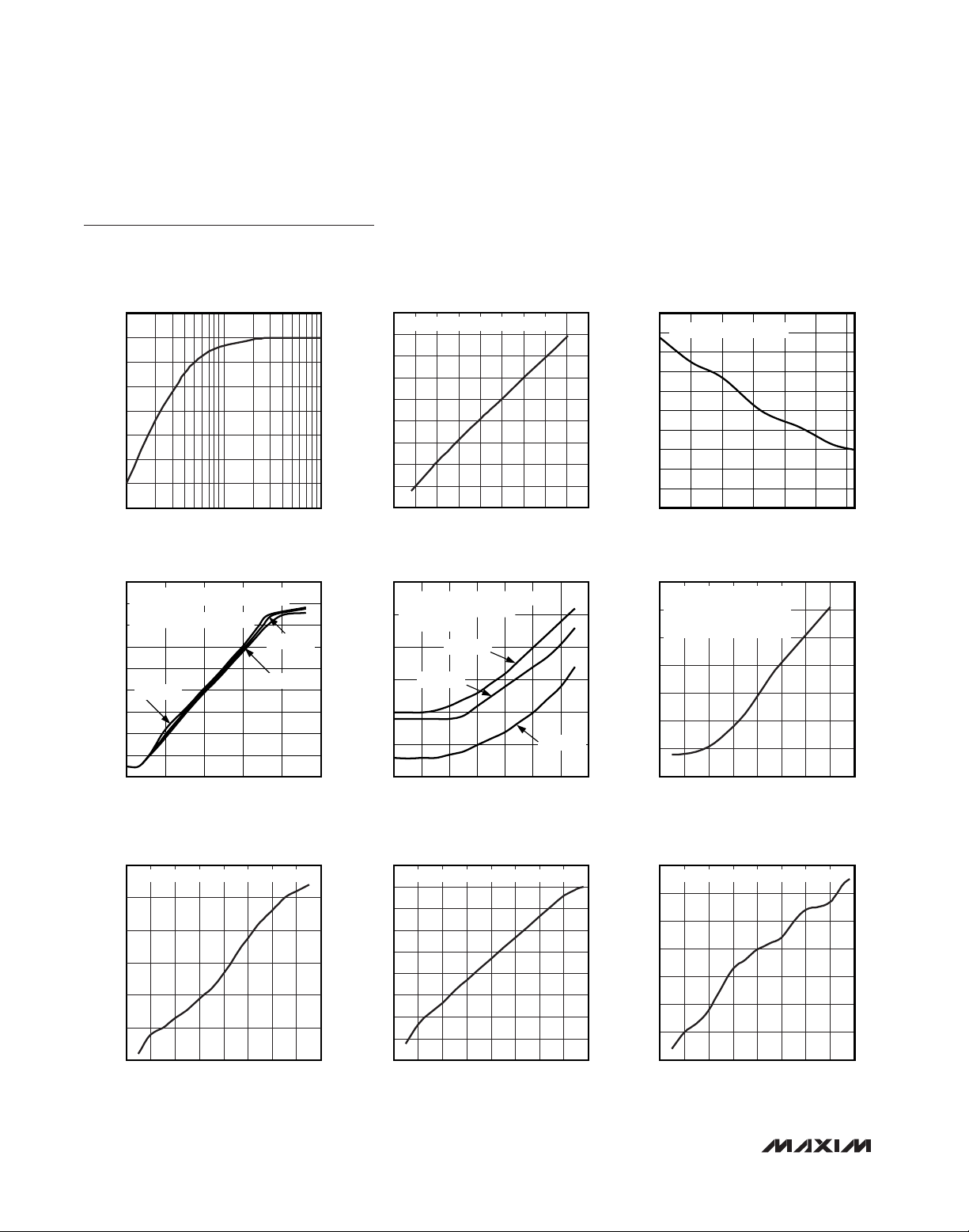
Typical Operating Characteristics (continued)
(MAX2112 Evaluation Kit: V
CC
= +3.3V, TA= +25°C, baseband output frequency = 5MHz; V
GC1
= +1.2V, default register settings
except BBG[3:0] = 1011.)
BASEBAND FILTER HIGHPASS
FREQUENCY RESPONSE
MAX2112 toc08
BASEBAND FREQUENCY (MHz)
BASEBAND OUTPUT LEVEL (dB)
1000
-10
-8
-4
-6
-2
0
2
-14
-12
100 10,000
PROGRAMMED f
-3dB
FREQUENCY
vs. MEASURED f
-3dB
FREQUENCY
MAX2112 toc09
PROGRAMMED f
-3dB
FREQUENCY (MHz)
MEASURED f
-3dB
FREQUENCY (MHz)
402015 25 30 35510
5
10
20
15
25
35
30
40
45
0
045
LPF[7:0] = 12 + (f
-3dB
- 4MHz)/290kHz
BASEBAND FILTER 3dB FREQUENCY
vs. TEMPERATURE
TEMPERATURE (°C)
BASEBAND GAIN ERROR AT f
-3dB
(dB)
MAX2112 toc10
-40-200 20406080
-1.0
-0.8
-0.6
-0.4
-0.2
0
0.2
0.4
0.6
0.8
1.0
NORMALIZED TO TA = +25°C
INPUT POWER vs. V
GC1
V
GC1
(V)
INPUT POWER (dBm)
MAX2112 toc11
0.5 1.0 1.5 2.0 2.5 3.0
-80
-70
-60
-50
-40
-30
-20
-10
0
10
ADJUST BBG[3:0] FOR 1V
P-P
BASEBAND
OUTPUT WITH
P
IN
= -75dBm AND V
GC1
= 0.5V
TA = -40°C
TA = +85°C
TA = +25°C
NOISE FIGURE vs. FREQUENCY
FREQUENCY (MHz)
NOISE FIGURE (dB)
MAX2112 toc12
900 1100 1300 1500 1700 1900 2100 2300
7.5
8.0
8.5
9.0
9.5
10.0
10.5
TA = +25°C
TA = +85°C
ADJUST BBG[3:0] FOR 1V
P-P
BASEBAND
OUTPUT WITH P
IN
= -75dBm
AND V
GC1
= 0.5V
TA = +70°C
NOISE FIGURE vs. INPUT POWER
MAX2112 toc13
INPUT POWER (dBm)
NOISE FIGURE (dB)
-20-30-40-50-60-70
20
10
30
40
50
60
70
0
-80 0-10
ADJUST BBG[3:0] FOR 1V
P-P
BASEBAND OUTPUT WITH
P
IN
= -75dBm AND V
GC1
= 0.5V.
f
LO
= 1500MHz
OUT-OF-BAND IIP3 vs. INPUT POWER
MAX2112 toc14
INPUT POWER (dBm)
OUT-OF-BAND IIP3 (dBm)
-20-30-40-50-60-70
-10
-20
0
10
20
30
-30
-80 0-10
SEE NOTE 4 ON PAGE 4 FOR CONDITIONS
IN-BAND IIP3 vs. INPUT POWER
MAX2112 toc15
INPUT POWER (dBm)
IN-BAND IIP3 (dBm)
-20-30-40-50-60-70
-30
-50
-40
-10
-20
0
10
20
30
-60
-80 0-10
SEE NOTE 3 ON PAGE 4 FOR CONDITIONS
IIP2 vs. INPUT POWER
MAX2112 toc16
INPUT POWER (dBm)
IIP2 (dBm)
-20-30-40-50-60-70
0
10
30
20
40
50
60
-10
-80 0-10
SEE NOTE 5 ON PAGE 4 FOR CONDITIONS

MAX2112
Complete, Direct-Conversion
Tuner for DVB-S2 Applications
_______________________________________________________________________________________
7
Typical Operating Characteristics (continued)
(MAX2112 Evaluation Kit: V
CC
= +3.3V, TA= +25°C, baseband output frequency = 5MHz; V
GC1
= +1.2V, default register settings
except BBG[3:0] = 1011.)
_______________________________________________________________________________________
7
0
-5
-10
-15
INPUT RETURN LOSS (dB)
-20
-25
900 2250
PHASE NOISE vs. OFFSET FREQUENCY
-90
-100
INPUT RETURN LOSS vs. FREQUENCY
-90
MAX2112 toc17
V
= 0.5V
GC1
V
= 2.7V
GC1
202518001350 15751125
FREQUENCY (MHz)
MAX2112 toc19
-95
-100
PHASE NOISE AT 10kHz OFFSET (dBc/Hz)
-105
925 1115 1305 1495 1685 1875 2065 2255
-70
-75
PHASE NOISE AT 10kHz OFFSET vs.
CHANNEL FREQUENCY
CHANNEL FREQUENCY (MHz)
LO LEAKAGE vs. LO FREQUENCY
MEASURED AT RF INPUT
MAX2112 toc18
MAX2112 toc20
-110
PHASE NOISE (dBc/Hz)
-120
fLO = 1800MHz
-130
1.0E+03 1.0E+06
OFFSET FREQUENCY (Hz)
1.0E+051.0E+04
450
400
350
300
250
200
KV (MHz/V)
150
100
50
0
-80
LO LEAKAGE (dBm)
-85
-90
925 1175 1425 1675 1925 2175
VCO: KV vs. VTUNE
SUB-BAND 23
SUB-BAND 12
SUB-BAND 0
0 0.5 1.0 1.5 2.0 2.5 3.0
VTUNE (V)
LO FREQUENCY (MHz)
MAX2112 toc21
MAX2112
Complete, Direct-Conversion
Tuner for DVB-S2 Applications
8 _______________________________________________________________________________________8 _______________________________________________________________________________________
Pin Description
PIN NAME FUNCTION
1 VCC_RF2
2 VCC_RF1
3 GND Ground. Connect to board’s ground plane for proper operation.
4 RFIN Wideband 75Ω RF Input. Connect to an RF source through a DC-blocking capacitor.
5 GC1
6 VCC_LO
7 VCC_VCO
8 VCOBYP
9 VTUNE
10 GNDTUNE Ground for VTUNE. Connect to the PCB ground plane.
11 GNDSYN Ground for Synthesizer. Connect to the PCB ground plane.
12 CPOUT
13 VCC_SYN
14 XTAL
DC Power Supply for LNA. Connect to a +3.3V low-noise supply. Bypass to GND with a 1nF capacitor
connected as close as possib l e to the pi n. D o not shar e capaci tor gr ound vi as w ith other g r ound connections.
DC Power Supply for LNA. Connect to a +3.3V low-noise supply. Bypass to GND with a 1nF capacitor
connected as close as possib l e to the pi n. D o not shar e capaci tor gr ound vi as w ith other g r ound connections.
RF Gain-Control Input. High-impedance analog input with a 0.5V to 2.7V operating range.
V
= 0.5V corresponds to the maximum gain setting.
GC1
DC Power Supply for LO Generation Circuits. Connect to a +3.3V low-noise supply. Bypass to GND with
a 1nF capacitor connected as close as possible to the pin. Do not share capacitor ground vias with
other ground connections.
DC Power Supply for VCO Circuits. Connect to a +3.3V low-noise supply. Bypass to GND with a 1nF
capacitor connected as close as possible to the pin. Do not share capacitor ground vias with other
ground connections.
Internal VCO Bias Bypass. Bypass to GND with a 100nF capacitor connected as close as possible to
the pin. Do not share capacitor ground vias with other ground connections.
High-Impedance VCO Tune Input. Connect the PLL loop filter output directly to this pin with as short of a
connection as possible.
C h ar g e - P um p O u tp u t . C o n n e c t t h i s o u t p u t t o t he P L L l o o p fi l t e r i n p u t w i t h th e s h or t e s t c o n n e ct i o n
p o ss i b l e .
DC Power Supply for Synthesizer Circuits. Connect to a +3.3V low-noise supply. Bypass to GND with a
1nF capacitor connected as close as possible to the pin. Do not share capacitor ground vias with other
ground connections.
Crystal-Oscillator Interface. Use with an external parallel-resonance-mode crystal through a series 1nF
capacitor. See the Typical Application Circuit.
15 REFOUT Crystal-Oscillator Buffer Output. A DC-blocking capacitor must be used when driving external circuitry.
DC Power Supply for Digital Logic Circuits. Connect to a +3.3V low-noise supply. Bypass to GND with a
16 VCC_DIG
17 QOUT+
18 QOUT-
19 IOUT+
20 IOUT-
21 IDC+
22 IDC-
23 QDC+
24 QDC-
25 VCC_BB
1nF capacitor connected as close as possible to the pin. Do not share capacitor ground vias with other
ground connections.
Quadrature Baseband Differential Output. AC-couple with 47nF capacitors to the demodulator input.
In-Phase Baseband Differential Output. AC-couple with 47nF capacitors to the demodulator input.
I-Channel Baseband DC Offset Correction. Connect a 47nF ceramic chip capacitor from IDC- to IDC+.
Q- C hannel Baseb and D C O ffset C or r ecti on. C onnect a 47nF cer am i c chi p cap aci tor fr om QD C - to QD C + .
DC Power Supply for Baseband Circuits. Connect to a +3.3V low-noise supply. Bypass to GND with
a 1nF capacitor connected as close as possible to the pin. Do not share capacitor ground vias with
other ground connections.

MAX2112
Complete, Direct-Conversion
Tuner for DVB-S2 Applications
_______________________________________________________________________________________ 9
Detailed Description
Register Description
The MAX2112 includes 12 user-programmable registers and 2 read-only registers. See Table 1 for register
configurations. The register configuration of Table 1
shows each bit name and the bit usage information for all
registers. Note that all registers must be written after and
no earlier than 100µs after the device is powered up.
_______________________________________________________________________________________ 9
Pin Description (continued)
Table 1. Register Configuration
X = Don’t care. 0 = Set to 0 for factory-tested operation. 1 = Set to 1 for factory-tested operation.
PIN NAME FUNCTION
26 SDA 2-Wire Serial-Data Interface. Requires ≥ 1kΩ pullup resistor to VCC.
27 SCL 2-Wire Serial-Clock Interface. Requires ≥ 1kΩ pullup resistor to VCC.
28 ADDR Address. Must be connected to either ground (logic 0) or supply (logic 1).
— EP Exposed Paddle. Solder evenly to the board’s ground plane for proper operation.
REG
NUMBER
R EG I ST ER
N A M E
1
2
3
4
5
6
7 PLL Write 0x06 D24 CPS ICP X X X X X
8 VCO Write 0x07 VCO[4] VCO[3] VCO[2] VCO[1] VCO[0] VAS ADL ADE
9 LPF Write 0x08 LPF[7] LPF[6] LPF[5] LPF[4] LPF[3] LPF[2] LP F[ 1] LPF[0]
10 Control Write 0x09 STBY X
11 Shutdown Write 0x0A X
12 Test Write 0x0B
13
14
N-Divider
MSB
N-Divider
LSB
Charge
Pump
F-Divider
MSB
F-Divider
LSB
XTAL
Divider
R-Divider
Status
Byte-1
Status
Byte-2
R EA D /
WR IT E
Write 0x00
Write 0x01 N[7] N[6] N[5] N[4] N[3] N[2] N[1] N[0]
Write 0x02
Write 0x03 F[15] F[14] F[13] F[12] F[11] F[10] F[9] F[8]
Write 0x04 F[7] F[6] F[5] F[4] F[3] F[2] F[1] F[0]
Write 0x05 XD[2] XD[1] XD[0] R[4] R[3] R[2] R[1] R[0]
Read 0x0C POR VASA VASE LD X X X X
Read 0x0D V C OS BR[4] V C OS BR[3] V C OS BR[2] V C OS BR[1] V C OS BR[0] AD C[ 2] AD C[ 1] AD C[ 0]
R EG
A D D R ESS
MSB LSB
D[7] D[6] D[5] D[4] D[3] D[2] D[1] D[0]
FRAC
1
CPMP[1]0CPMP[0]0CPLIN[1]0CPLIN[0]
CPTST[2]0CPTST[1]0CPTST[0]
DATA BYTE
N[14] N[13] N[12] N[11] N[10] N[9] N[8]
F[19] F[18] F[17] F[16]
BB
TURBO
RFMIX0RFVGA0FE
0
LD
M U X[ 2]
1
0
LD
M U X[ 1]
0
M U X[ 0]
0
LD
0
PLL
0
PWDN
0
DIV
0
0
1
X BBG[3] BBG[ 2] BBG[ 1] BBG[ 0]
VCO
0
X
MAX2112
Complete, Direct-Conversion
Tuner for DVB-S2 Applications
10 ______________________________________________________________________________________
Table 2. N-Divider MSB Register
Table 3. N-Divider LSB Register
Table 4. Charge-Pump Register
Table 5. F-Divider MSB Register
Table 6. F-Divider LSB Register
Table 7. XTAL Buffer and Reference Divider Register
BIT NAME BIT LOCATION (0 = LSB) DEFAULT FUNCTION
FRAC 7 1 Users must program to 1 upon powering up the device.
N[14:8] 6–0 0000000
BIT NAME BIT LOCATION (0 = LSB) DEFAULT FUNCTION
N[7:0] 7–0 00100011
BIT NAME BIT LOCATION (0 = LSB) DEFAULT FUNCTION
CPMP[1:0] 7–6 00
CPLIN[1:0] 5–4 00
F[19:16] 3–0 0010
Sets the most significant bits of the PLL integer-divide number (N). N can
range from 19 to 251.
Sets the least significant bit s of the PLL integer-divide number. N can range
from 19 to 251.
Charge-pump minimum pulse width. Users must program to 00 upon
powering up the device.
Controls charge-pump linearity. Users must program to 01 upon powering up
the device.
S ets the 4 m ost si g ni fi cant b i ts of the P LL fr acti onal d i vi d e num b er .
D efaul t val ue i s F = 194,180 d eci m al .
BIT NAME BIT LOCATION (0 = LSB) DEFAULT FUNCTION
F[15:8] 7–0 11110110
S ets the m ost si g ni fi cant b i ts of the P LL fr acti onal - d i vi d e num b er ( F) .
D efaul t val ue i s F = 194,180 d eci m al .
BIT NAME BIT LOCATION (0 = LSB) DEFAULT FUNCTION
F[7:0] 7–0 10000100
S ets the l east si g ni fi cant b i ts of the P LL fr acti onal - d i vi d e num b er ( F) .
D efaul t val ue i s F = 194,180 d eci m al .
BIT NAME BIT LOCATION (0 = LSB) DEFAULT FUNCTION
Sets the crystal-divider setting.
000 = Divide by 1.
001 = Divide by 2.
XD[2:0] 7–5 000
R[4:0] 4–0 00001
011 = Divide by 3.
100 = Divide by 4.
101 through 110 = All divide values from 5 (101) to 7 (110).
111 = Divide by 8.
Sets the PLL reference-divider (R) number. Users must program to 00001
upon powering up the device.
00001 = Divide by 1; other values are not tested.

MAX2112
Complete, Direct-Conversion
Tuner for DVB-S2 Applications
______________________________________________________________________________________ 11
Table 8. PLL Register
Table 9. VCO Register
Table 10. Lowpass Filter Register
BIT NAME BIT LOCATION (0 = LSB) DEFAULT FUNCTION
VCO divider setting.
D24 7 1
CPS 6 1
ICP 5 0
X 4–0 X Don’t care.
0 = Divide by 2. Use for LO frequencies ≥ 1125MHz.
1 = Divide by 4. Use for LO frequencies < 1125MHz.
Charge-pump current mode.
0 = Charge-pump current controlled by ICP bit.
1 = Charge-pump current controlled by VCO autoselect (VAS).
Charge-pump current.
0 = 600µA typical.
1 = 1200µA typical.
BIT NAME BIT LOCATION (0 = LSB) DEFAULT FUNCTION
VCO[4:0] 7–3 11001
VAS 2 1
ADL 1 0
ADE 0 0
C ontr ol s w hi ch V C O i s acti vated w hen usi ng m anual V C O p r og r am m i ng m od e.
Thi s al so ser ves as the st ar ti ng p oi nt for the V C O autosel ecti on ( V AS ) m od e.
VCO autoselection (VAS) circuit.
0 = Disable VCO selection must be programmed through I
1 = Enable VCO selection controlled by autoselection circuit.
Enables or disables the VCO tuning voltage ADC latch when the VCO
autoselect mode (VAS) is disabled.
0 = Disables the ADC latch.
1 = Latches the ADC value.
Enables or disables VCO tuning voltage ADC read when the VCO autoselect
mode (VAS) is disabled.
0 = Disables ADC read.
1 = Enables ADC read.
2
C.
BIT NAME BIT LOCATION (0 = LSB) DEFAULT FUNCTION
Sets the baseband lowpass filter 3dB corner frequency.
LPF[7:0] 7–0 01001011
f
= 4MHz + (LPF[7:0]
-3dB
Default value equates to f
- 12) x 290kHz.
dec
= 22.27MHz typical.
-3dB

MAX2112
Complete, Direct-Conversion
Tuner for DVB-S2 Applications
12 ______________________________________________________________________________________
Table 11. Control Register
Table 12. Shutdown Register
BIT NAME BIT LOCATION (0 = LSB) DEFAULT FUNCTION
Software standby control.
STBY 7 0
X 6 X Don’t care.
PWDN 5 0
X 4 X Don’t care.
BBG[3:0] 3-0 0000
BIT NAME BIT LOCATION (0 = LSB) DEFAULT FUNCTION
X 7 X Don’t care.
PLL 6 0
DIV 5 0
VCO 4 0
BB 3 0
RFMIX 2 0
RFVGA 1 0
FE 0 0
0 = Normal operation.
1 = D i sab l es the si g nal p ath and fr eq uency synthesi zer l eavi ng onl y the 2- w i r e
b us, cr ystal osci l l ator , X TALOU T b uffer , and X TALOU T b uffer d i vi d er acti ve.
Factory use only.
0 = Normal operation;
other value is not tested.
Baseband gain setting (1dB typical per step).
0000 = Minimum gain (0dB, default).
…
1111 = Maximum gain (15dB typical).
PLL enable.
0 = Normal operation.
1 = Shuts down the PLL. Value not tested.
Divider enable.
0 = Normal operation.
1 = Shuts down the divider. Value not tested.
VCO enable.
0 = Normal operation.
1 = Shuts down the VCO. Value not tested.
Baseband enable.
0 = Normal operation.
1 = Shuts down the baseband. Value not tested.
RF mixer enable.
0 = Normal operation.
1 = Shuts down the RF mixer. Value not tested.
RF VGA enable.
0 = Normal operation.
1 = Shuts down the RF VGA. Value not tested.
Front-end enable.
0 = Normal operation.
1 = Shuts down the front-end. Value not tested.

MAX2112
Complete, Direct-Conversion
Tuner for DVB-S2 Applications
______________________________________________________________________________________ 13
Table 13. Test Register
Table 14. Status Byte-1 Register
Table 15. Status Byte-2 Register
BIT NAME BIT LOCATION (0 = LSB) DEFAULT FUNCTION
CPTST[2:0] 7–5 000
X 4 X Don’t care.
TURBO 3 0
LDMUX[2:0] 2 –0 000
Charge-pump test modes.
000 = Normal operation (default).
Charge-pump fast lock.
Users must program to 1 after powering up the device.
REFOUT output.
000 = Normal operation. Other values are not tested.
BIT NAME BIT LOCATION (0 = LSB) FUNCTION
Power-on reset status.
POR 7
VASA 6
VASE 5
LD 4
X 3:0 Don’t care.
0 = Chip status register has been read with a stop condition since last power-on.
1 = Power-on reset (power cycle) has occurred. Default values have been loaded in
registers.
Indicates whether VCO autoselection was successful.
0 = Indicates the autoselect function is disabled or unsuccessful VCO selection.
1 = Indicates successful VCO autoselection.
Status indicator for the autoselect function.
0 = Indicates the autoselect function is active.
1 = Indicates the autoselect process is inactive.
PLL lock detector. TURBO bit must be programmed to 1 for valid LD reading.
0 = Unlocked.
1 = Locked.
BIT NAME BIT LOCATION (0 = LSB) FUNCTION
VCOSBR[4:0] 7-3 VCO band readback.
VAS ADC output readback.
000 = Out of lock.
001 = Locked.
ADC[2:0] 2-0
010 = VAS locked.
101 = VAS locked.
110 = Locked.
111 = Out of lock.
MAX2112
2-Wire Serial Interface
The MAX2112 uses a 2-wire I2C-compatible serial interface consisting of a serial-data line (SDA) and a serialclock line (SCL). SDA and SCL facilitate bidirectional
communication between the MAX2112 and the master
at clock frequencies up to 400kHz. The master initiates
a data transfer on the bus and generates the SCL signal to permit data transfer. The MAX2112 behaves as a
slave device that transfers and receives data to and
from the master. SDA and SCL must be pulled high
with external pullup resistors (1kΩ or greater) for proper
bus operation. Pullup resistors should be referenced to
the MAX2112’s VCC.
One bit is transferred during each SCL clock cycle. A
minimum of nine clock cycles is required to transfer a
byte in or out of the MAX2112 (8 bits and an ACK/NACK).
The data on SDA must remain stable during the high
period of the SCL clock pulse. Changes in SDA while
SCL is high and stable are considered control signals
(see the
START and STOP Conditions
section). Both SDA
and SCL remain high when the bus is not busy.
START and STOP Conditions
The master initiates a transmission with a START condition (S), which is a high-to-low transition on SDA while
SCL is high. The master terminates a transmission with
a STOP condition (P), which is a low-to-high transition
on SDA while SCL is high.
Acknowledge and Not-Acknowledge Conditions
Data transfers are framed with an acknowledge bit
(ACK) or a not-acknowledge bit (NACK). Both the master and the MAX2112 (slave) generate acknowledge
bits. To generate an acknowledge, the receiving device
must pull SDA low before the rising edge of the
acknowledge-related clock pulse (ninth pulse) and
keep it low during the high period of the clock pulse.
To generate a not-acknowledge condition, the receiver
allows SDA to be pulled high before the rising edge of
the acknowledge-related clock pulse, and leaves SDA
high during the high period of the clock pulse.
Monitoring the acknowledge bits allows for detection of
unsuccessful data transfers. An unsuccessful data
transfer happens if a receiving device is busy or if a
system fault has occurred. In the event of an unsuccessful data transfer, the bus master must reattempt
communication at a later time.
Slave Address
The MAX2112 has a 7-bit slave address that must be
sent to the device following a START condition to initiate communication. The slave address is internally programmed to 1100000. The eighth bit (R/W) following
the 7-bit address determines whether a read or write
operation occurs.
The MAX2112 continuously awaits a START condition
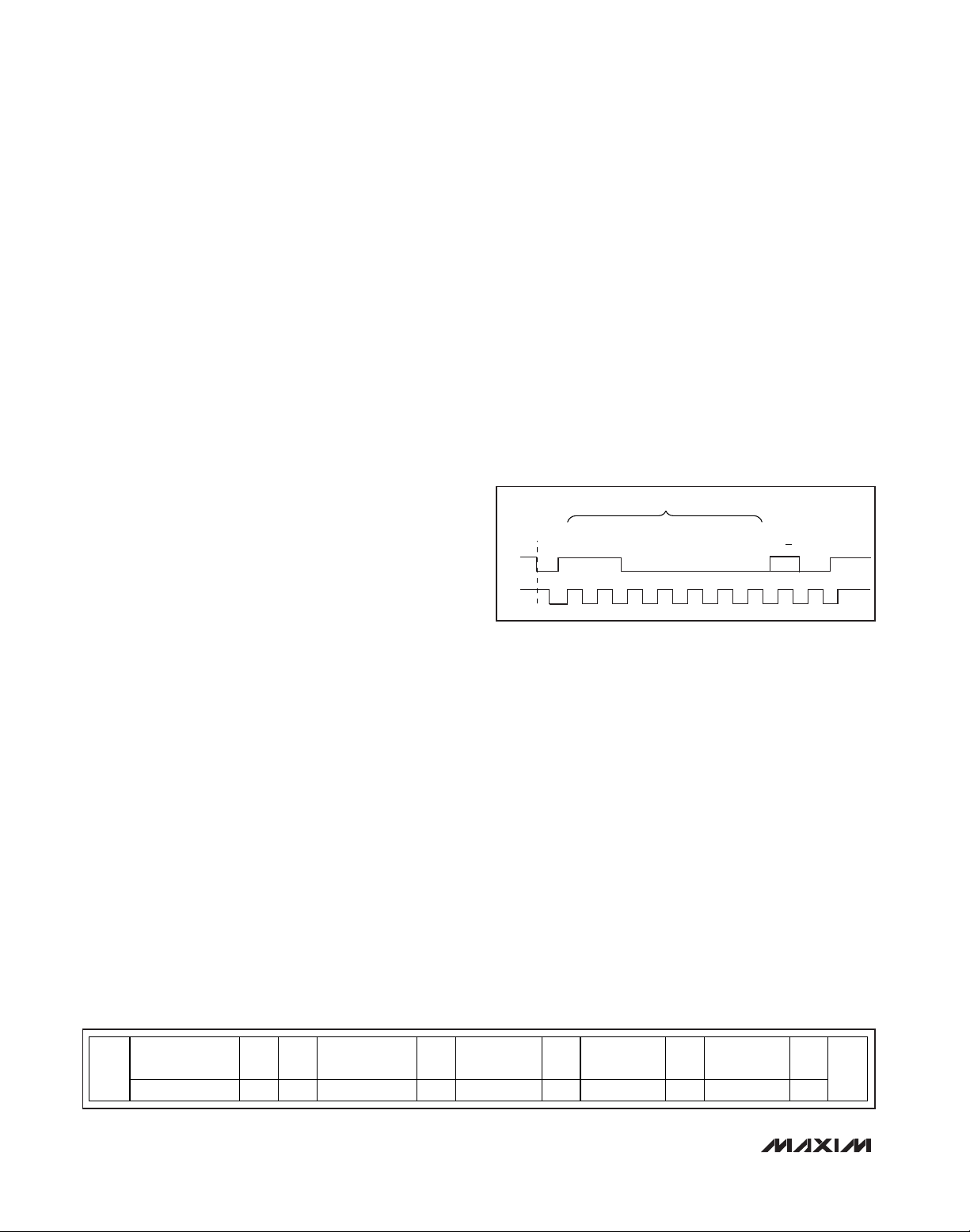
followed by its slave address. When the device recognizes its slave address, it acknowledges by pulling the
SDA line low for one clock period; it is ready to accept
or send data depending on the R/W bit (Figure 1).
The write/read address is C0/C1 if ADDR pin is connected to ground. The write/read address is C2/C3 if
ADDR pin is connected to VCC.
Write Cycle
When addressed with a write command, the MAX2112
allows the master to write to a single register or to multiple successive registers.
A write cycle begins with the bus master issuing a
START condition followed by the seven slave address
bits and a write bit (R/W = 0). The MAX2112 issues an
ACK if the slave address byte is successfully received.
The bus master must then send to the slave the address
of the first register it wishes to write to (see Table 1 for
register addresses). If the slave acknowledges the
address, the master can then write one byte to the register at the specified address. Data is written beginning
with the most significant bit. The MAX2112 again issues
an ACK if the data is successfully written to the register.
The master can continue to write data to the successive
internal registers with the MAX2112 acknowledging each
successful transfer, or it can terminate transmission by
issuing a STOP condition. The write cycle does not terminate until the master issues a STOP condition.
Complete, Direct-Conversion
Tuner for DVB-S2 Applications
14 ______________________________________________________________________________________
Figure 1. MAX2112 Slave Address Byte with ADDR Pin
Connected to Ground
Figure 2. Example: Write Registers 0 through 2 with 0x0E, 0xD8, and 0xE1, respectively.
SLAVE ADDRESS
1100000
S
SDA
SCL
1 234567
ACK
R/W
89
WRITE DEVICE
START
ADDRESS
1100000 0 — 0x00 — 0x0E — 0xD8 — 0xE1 —
R/W ACK
WRITE REGISTER
ADDRESS
ACK
WRITE DATA TO
REGISTER 0x00
ACK
WRITE DATA TO
REGISTER 0x01
ACK
WRITE DATA TO
REGISTER 0x02
ACK
STOP

Read Cycle
When addressed with a read command, the MAX2112
allows the master to read back a single register, or multiple successive registers.
A read cycle begins with the bus master issuing a
START condition followed by the 7 slave address bits
and a write bit (R/W = 0). The MAX2112 issues an ACK if
the slave address byte is successfully received. The bus
master must then send the address of the first register it
wishes to read (see Table 1 for register addresses). The
slave acknowledges the address. Then, a START condition is issued by the master, followed by the 7 slave
address bits and a read bit (R/W = 1). The MAX2112
issues an ACK if the slave address byte is successfully
received. The MAX2112 starts sending data MSB first
with each SCL clock cycle. At the 9th clock cycle, the
master can issue an ACK and continue to read successive registers, or the master can terminate the transmission by issuing a NACK. The read cycle does not
terminate until the master issues a STOP condition.
Figure 3 illustrates an example in which registers 0
through 2 are read back.
Application Information
The MAX2112 downconverts RF signals in the 925MHz to
2175MHz range directly to the baseband I/Q signals. The
devices are targeted for digital DBS tuner applications.
RF Input
The RF input of the MAX2112 is internally matched to
75Ω. Only a DC-blocking capacitor is needed. See the
Typical Application Circuit
.
RF Gain Control
The MAX2112 features a variable-gain low-noise amplifier providing 73dB of RF gain range. The voltage control (VGC) range is 0.5V (minimum attenuation) to 2.7V
(maximum attenuation).
Baseband Variable-Gain Amplifier
The receiver baseband variable-gain amplifiers provide
15dB of gain control range programmable in 1dB
steps. The VGA gain can be serially programmed
through the SPI interface by setting bits BBG[3:0] in the
Control register.
Baseband Lowpass Filter
The MAX2112 includes a programmable on-chip
7th-order Butterworth filter. The filter -3dB corner frequency can be adjusted from approximately 4MHz to
40MHz by programming the LPF[7:0] register using the
following equation:
LPF[7:0]
dec
= (f
-3dB
- 4MHz)/0.29MHz + 12,
where f
-3dB
is in units of MHz.
Total device supply current depends on the filter BW
setting. See Supply Current vs. Baseband Filter Cutoff
Frequency in the
Typical Operating Characteristics
for
more information.
DC Offset Cancellation
The DC offset cancellation is required to maintain the
I/Q output dynamic range. Connecting an external
capacitor between IDC+ and IDC- forms a highpass filter for the I channel and an external capacitor between
QDC+ and QDC- forms a highpass filter for the Q channel. Keep the value of the external capacitor less than
47nF to form a typical highpass corner of 250Hz.
XTAL Oscillator
The MAX2112 contains an internal reference oscillator,
reference output divider, and output buffer. All that is
required is to connect a crystal through a series 1nF
capacitor. To minimize parasitics, place the crystal and
series capacitor as close as possible to pin 14 (XTAL
pin). See Table 16 for crystal (XTAL) ESR (equivalent
series resistance) requirements.
VCO Autoselect (VAS)
The MAX2112 includes 24 VCOs. The local oscillator
frequency can be manually selected by programming
the VCO[4:0] bits in the VCO register. The selected VCO
is reported in the Status Byte-2 register (see Table 15).
MAX2112
Complete, Direct-Conversion
Tuner for DVB-S2 Applications
______________________________________________________________________________________ 15
Figure 3. Example: Receive Data from Read Registers
Table 16. Maximum Crystal ESR
Requirement
S
DEVICE
T
ADDRESS
A
R
1100000
T
R / W
A
C
K
REGISTER
ADDRESS
000000000
S
T
A
R
T
DEVICE
ADDRESS
1100000 1
A
C
K
R / W
REG 00
A
DATA
C
K
xxxxxxxx
REG 01
A
DATA
C
K
xxxxxxxx
REG 02
A
DATA
C
K
xxxxxxxx
S
N
T
A
O
C
P
K
ESR
() XTAL FREQUENCY (MHz)
MAX
80 12 < f
60 14 < f
XTAL
XTAL
14
30

MAX2112
Alternatively, the MAX2112 can be set to autonomously
choose a VCO by setting the VAS bit in the VCO register to logic-high. The VAS routine is initiated once the
F-Divider LSB register word (REG 5) is loaded.
In the event that only the N-divider register or
F-divider MSB word is changed, the F-divider LSB
word must also be loaded last to initiate the VCO
autoselect function. The VCO value programmed in the
VCO[4:0] register serves as the starting point for the automatic VCO selection process.
During the selection process, the VASE bit in the Status
Byte-1 register is cleared to indicate the autoselection
function is active. Upon successful completion, bits VASE
and VASA are set and the VCO selected is reported in the
Status Byte-2 register (see Table 15). If the search is
unsuccessful, VASA is cleared and VASE is set. This indicates that searching has ended but no good VCO has
been found, and occurs when trying to tune to a frequency outside the VCO’s specified frequency range.
Refer to the MAX2112/MAX2120 VCO Autoselect (VAS)
Application Note for more information.
3-Bit ADC
The MAX2112 has an internal 3-bit ADC connected to
the VCO tune pin (VTUNE). This ADC can be used for
checking the lock status of the VCOs.
Table 17 summarizes the ADC output bits and the VCO
lock indication. The VCO autoselect routine only selects
a VCO in the “VAS locked” range. This allows room for
a VCO to drift over temperature and remain in a valid
“locked” range.
The ADC must first be enabled by setting the ADE bit in
the VCO register. The ADC reading is latched by a subsequent programming of the ADC latch bit (ADL = 1).
The ADC value is reported in the Status Byte-2 register
(see Table 15).
Standby Mode
The MAX2112 features normal operating mode and
standby mode using the I
2
C interface. Setting a logichigh to the STBY bit in the Control register puts the
device into standby mode, during which only the 2wire-compatible bus, the crystal oscillator, the XTAL
buffer, and the XTAL buffer divider are active.
In all cases, register settings loaded prior to entering
shutdown are saved upon transition back to active
mode. Default register values are provided for the
user’s convenience only. It is the user’s responsibility to
load all the registers no sooner than 100µs after the
device is powered up.
Layout Considerations
The MAX2112 EV kit serves as a guide for PCB layout.
Keep RF signal lines as short as possible to minimize
losses and radiation. Use controlled impedance on all
high-frequency traces. For proper operation, the
exposed paddle must be soldered evenly to the board’s
ground plane. Use abundant vias beneath the exposed
paddle for maximum heat dissipation. Use abundant
ground vias between RF traces to minimize undesired
coupling. Bypass each VCCpin to ground with a 1nF
capacitor placed as close as possible to the pin.
Complete, Direct-Conversion
Tuner for DVB-S2 Applications
16 ______________________________________________________________________________________
Table 17. ADC Trip Points and Lock Status
ADC[2:0] LOCK STATUS
000 Out of lock
001 Locked
010 VAS locked
101 VAS locked
110 Locked
111 Out of lock

MAX2112
Complete, Direct-Conversion
Tuner for DVB-S2 Applications
______________________________________________________________________________________ 17
Typical Application Circuit
RF INPUT
V
GC
SERIAL-DATA
INPUT/OUTPUT
SERIAL-CLOCK
INPUT
SCL
V
CC
V
V
CC
VCC_RF2
CC
VCC_RF1
GND
RFIN
GC1
VCC_LO
V
CC
VCC_VCO
+
1
2
3
4
5
6
7
ADDR
28
INTERFACE LOGIC
AND CONTROL
DIV2
/DIV4
EP
SDA
26 24 23
27
VCC_BB
25
MAX2112
LPF BW
CONTROL
FREQUENCY
SYNTHESIZER
V
CC
QDC-
DC OFFSET
CORRECTION
QDC+
IDC-
22
21
20
19
18
17
16
15
IDC+
IOUT-
IOUT+
QOUT-
QOUT+
VCC_DIG
REFOUT
BASEBAND
OUTPUTS
V
CC
8
VCOBYP
9
VTUNE
GNDTUNE
11 13
GNDSYN
CPOUT
V
CC
14
XTAL
VCC_SYN
10 12

MAX2112
Complete, Direct-Conversion
Tuner for DVB-S2 Applications
18 ______________________________________________________________________________________
Chip Information
PROCESS: BiCMOS
Package Information
For the latest package outline information and land patterns, go
to www.maxim-ic.com/packages
. Note that a “+”, “#”, or “-” in
the package code indicates RoHS status only. Package drawings may show a different suffix character, but the drawing pertains to the package regardless of RoHS status.
PACKAGE
TYPE
PACKAGE
CODE
OUTLINE
NO.
LAND
PATTERN NO.
28 TQFN-EP T2855+3
21-0140 90-0023

MAX2112
Complete, Direct-Conversion
Tuner for DVB-S2 Applications
Maxim cannot assume responsibility for use of any circuitry other than circuitry entirely embodied in a Maxim product. No circuit patent licenses are
implied. Maxim reserves the right to change the circuitry and specifications without notice at any time.
Maxim Integrated Products, 120 San Gabriel Drive, Sunnyvale, CA 94086 408-737-7600 ____________________
19
© 2010 Maxim Integrated Products Maxim is a registered trademark of Maxim Integrated Products, Inc.
Revision History
REVISION
NUMBER
0 8/07 Initial release —
1 12/07 Corrected errors in data sheet 1–7, 9–16
2 5/10
REVISION
DATE
DESCRIPTION
Corrected errors in FUNCTION cells of Tables 8 and 10, corrected formula in
Baseband Lowpass Filter section
PAGES
CHANGED
11, 15
 Loading...