

19-0298; Rev 4; 5/96
EVALUATION KIT
AVAILABLE
6-Bit Quadrature Digitizer
_______________General Description
The MAX2101 6-bit quadrature digitizer combines quadrature demodulation with analog-to-digital conversion on
a single bipolar silicon die. This unique RF-to-Bits
TM
function bridges the gap between existing RF downconverters and CMOS digital signal processors (DSPs).
The MAX2101’s simple receiver subsystem is designed
for digital communications systems such as those used
in DBS, TVRO, WLAN, and other applications.
The MAX2101 accepts input signals from 400MHz to
700MHz and applies adjustable gain, providing at least
40dB of dynamic range.
Each baseband is filtered by an on-chip, 5th-order
Butterworth lowpass filter, or the user can select an
external filter path. Baseband sample rate is 60Msps.
The MAX2101 is available in a commercial temperature
range, 100-pin MQFP package.
________________________Applications
Recovery of PSK and QAM Modulated RF Carriers
Direct-Broadcast Satellite (DBS) Systems
Television Receive-Only (TVRO) Systems
Cable Television (CATV) Systems
Wireless Local Area Networks (WLANs)
____________________________Features
♦ ADCs Provide Greater than 5.5 Effective Bits at
fS= 60Msps, fIN= 15MHz
♦ Fully Integrated Lowpass Filters with
Externally Variable Bandwidth (10MHz to 30MHz)
♦ 40dB Dynamic Range
♦ Integrated VCO and Quadrature Generation
Network for I/Q Demodulation
♦ Divide-by-16 Prescaler for Oscillator PLL
♦ Programmable Counter for Variable Sample Rates
♦ Signal-Detection Function
♦ Selectable Offset Binary or Twos-Complement
Output Data Format
♦ Automatic Baseband Offset Cancellation
______________Ordering Information
PART
MAX2101CMQ 0°C to +70°C
TEMP. RANGE PIN-PACKAGE
100 MQFP
MAX2101
__________________________________________________Typical Application Circuit
LOW-NOISE AMPLIFIER
X/KU BAND
QUADRATURE
GENERATION
612MHz PHASE LOCKED
TM
RF-to-Bits is a registered trademark of Tektronix, Inc.
H POLARIZATION
V POLARIZATION
950MHz to 2000MHz
LOCAL OSCILLATOR
LOW-NOISE BLOCK
0°
90°
DIV-16
________________________________________________________________
MAX2101
A/D
CONVERSION
LOCAL OSCILLATOR
L-BAND DOWNCONVERTER
CLOCK
MATCHED
FILTERS
AND
CARRIER
RECOVERY
600MHz
(NARROW BAND)
ERROR
DETECTION
AND
CORRECTION
Maxim Integrated Products
MISCELLANEOUS
DSP
DSP POST PROCESSING
1
For free samples & the latest literature: http://www.maxim-ic.com, or phone 1-800-998-8800

6-Bit Quadrature Digitizer
ABSOLUTE MAXIMUM RATINGS
Supply Voltage Ranges (Note 1)
...................................................................(-0.3V to +6.5V)
V
CC
.....................................................................(V
V
INA
....................................................................(V
V
IND
CCA
CCD
+ 0.3V)
+ 0.3V)
Continuous Power Dissipation (T
Operating Temperature Range...............................0°C to +70°C
Storage Temperature Range.............................-65°C to +150°C
Lead Temperature (soldering, <10sec)...........................+300°C
Note 1: The digital control inputs are diode protected; however, permanent damage may occur on unconnected units under high-
energy electrostatic fields. Keep unused units in conductive foam or shunt the terminals together. Discharge the conductive
foam to the destination socket before insertion.
Stresses beyond those listed under “Absolute Maximum Ratings” may cause permanent damage to the device. These are stress ratings only, and functional
MAX2101
operation of the device at these or any other conditions beyond those indicated in the operational sections of the specifications is not implied. Exposure to
absolute maximum rating conditions for extended periods may affect device reliability.
ELECTRICAL CHARACTERISTICS
(VCC= 4.75V to 5.25V, TA= +25°C, unless otherwise noted.)
CONDITIONS
DC SPECIFICATIONS (V
Digital Supply Current
ADC Supply Current
RF Blocks Supply Current
IF Port DC Dynamic Range
IF Port Input Resistance
AGC Input Voltage
AGC Input Resistance
AGC Input Capacitance
AGC Control Slope Variation
AGC Control Input Bias Current
Lowpass Filter Tune Input Resistance
Lowpass Filter Tune Input Capacitance
TNKA, TNKB Resonant Port Bias Voltage
LO Resonant Port Input Resistance
LO Resonant Port Input Capacitance
LO Prescaler Output High (Note 3)
LO Prescaler Output Low
LO Prescaler Output Source Current
LO Prescaler Output Sink Current
Baseband Amplifier DC Gain A
Baseband Input—Input Capacitance C
Baseband Amplifier I/Q Offset Match
(Note 4)
Baseband Amplifier Offset Adjust
Input Resistance
= System Ground, V
GND
CCD
CCAD
CCRF
AGMIN
AGMAX
AGC
AGC
AGC
AGC
ILPF
ILPF
LO
ILO
ILO
OH
OL
OH
OL
VBB
IBB
V
OFFBB
R
OFFBB
= V
CCA
V
CCA
V
CCAD
V
CCIF
IF
IF
CCD
, V
, V
CCO
CC2
= 5.0V ±5%)
, V
, V
CCD
, V
, V
CC1
CCQ
CCC
VIF= 100mV
VIF= 0.5mV 2.3 2.9V
(Note 2) pF2C
Variation dB/V
Voltage range = 1V to 4V
(Note 2)
4.1V on complementary input V13V
(Note 2)
(Note 2)
RL= 1MΩ, CL= 15pF
RL= 1MΩ, CL= 15pF
RL= 1MΩ, CL= 15pF, VO= 2.4V
RL= 1MΩ, CL= 15pF, VO= 0.5V
(Note 2) 2 pF
LSB = 24mV, ENOPB = 0V,
V
FTUNE
= V
FTMIN
to V
FTMAX
Voltage Range = 1V to 4V 10 kΩ
= +70°C).......................1.6W
A
1.0 1.5V
4:1SV
27 29 31 dB
1.0 LSB
UNITSMIN TYP MAXSYMBOLPARAMETER
mA102I
mA80I
mA170I
mV0.5 100V
Ω40 75R
V
kΩ50 100R
dB40AGCRAGC Range
µA±20I
kΩ10R
pF2C
kΩ10R
pF2C
V2.4V
V0.5V
µA400I
µA50I
2 _______________________________________________________________________________________

6-Bit Quadrature Digitizer
ELECTRICAL CHARACTERISTICS (continued)
(VCC= 4.75V to 5.25V, TA= +25°C, unless otherwise noted.)
V
Power Detect Output Minimum
Power Detect Output Maximum
ADC Amplitude Response Match
ADC Input Offset
OFFAD
RF Signal Path DC Gain
Composite I/Q Gain Mismatch
Buffered Reference Voltage
(Zero Temperature Coefficient)
Buffered Reference Voltage
(Proportional to Absolute Temperature)
V
Temperature Coefficient
PTAT
Buffered Reference Voltage
(2 x VREF)
Data Output High (Note 3)
Data Output Low
Data Output Source Current (Note 3)
Data Output Sink Current
Data Clock Output High (Note 3)
Data Clock Output Low
Data Clock Output Source Current (Note 3)
Data Clock Output Sink Current
Master Clock Input Dynamic Range
Master Clock Input Resistance
Master Clock Input Capacitance
Reference Clock Output High (Note 3)
Reference Clock Output Low
Reference Clock Output Source Current
(Note 3)
Reference Clock Output Sink Current
Digital Input High Threshold (Note 5) V
Digital Input Low Threshold (Note 5) V
Digital Input Current High (Note 5) I
Digital Input Current Low (Note 5) I
FLTRSEL Input Current High I
FLTRSEL Input Current Low I
PWR
PWR
VM
VRF
(IQ)
REF
PTAT
2R5
OH
OL
OH
OL
OH
OL
OH
OL
MCLK
IMCLK
IMCLK
OH
OL
OH
OL
IH
IL
IH
IL
IH
IL
= 0V
p-p
> 2V DC
V
OBB
OBB
Channel to channel dB0.4A
LSB = 24mV, either channel
AGC set to maximum gain dB63A
Entire signal path, DC,
V
FTUNEI
= V
FTUNEQ
RL= 1kΩ, CL= 0.1µF
RL= 40kΩ,
CL= 0.01µF
TA= 0°C to +70°C mV/°C4.5
Ratio of V
2R5
RL= 1MΩ, CL= 15pF
RL= 1MΩ, CL= 15pF
RL= 1MΩ, CL= 15pF, VO= 2.4V
RL= 1MΩ, CL= 15pF, VO= 0.5V
RL= 1MΩ, CL= 15pF
RL= 1MΩ, CL= 15pF
RL= 1MΩ, CL= 15pF, VO= 2.4V
RL= 1MΩ, CL= 15pF, VO= 0.5V
RL= 50Ω external, f = 5MHz
RL= 10MΩ, CL= 15pF
RL= 10MΩ, CL= 15pF
RL= 1MΩ, CL= 15pF, VO= 2.4V
RL= 1MΩ, CL= 15pF, VO= 0.5V µA50I
VIH= 2.0V -150 -500 µA
VIL= 0.8V -400 -790 µA
VIH= 2.0V µA
VIL= 0.8V µA
CONDITIONS
= V
2R5
TA= +25°C 1.0 1.3
TA= 0°C to +70°C
(Note 2)
to V
REF
UNITSMIN TYP MAXSYMBOLPARAMETER
mV21 25LSBADC LSB Size
LSB0.5V
LSB1.0DNLADC Differential Nonlinearity
LSB1.0INLADC Integral Nonlinearity
0.9 1.5
1.9 2.1V
dBm010P
2.0 V
0.8 V
MAX2101
V1.5V
V3.75V
dB0.5∆M
V1.18 1.25V
VV
V
V2.2V
V0.5V
µA400I
µA50I
V2.2V
V0.5V
µA400I
µA50I
kΩ2R
pF5C
V2.2V
V0.5V
µA400I
_______________________________________________________________________________________ 3

6-Bit Quadrature Digitizer
ELECTRICAL CHARACTERISTICS (continued)
(VCC= 4.75V to 5.25V, TA= +25°C, unless otherwise noted.)
CONDITIONS
AC SPECIFICATIONS (GND = System Ground, VCC= V
IF Port Dynamic Range (Notes 2, 6)
RS= 50Ω, fIF= 400MHz to 700MHz dBm-50 -10P
IF
RS= 50Ω, R
network, fIF= 400MHz to 700MHz
IF Input Frequency Range
MAX2101
(Note 2) MHz400 700f
IF
R
gain configured for PIF= -50dBm
Noise Figure Variation
NF
Maximum gain to minimum gain dB/dB1∆
Gain configured for PIF= -10dBm,
f
BB1
Gain configured for PIF= -50dBm,
f
BB1
External resonator, guaranteed MHz400 700f
10MHz off fC, 1Hz bandwidth
N
10kHz off fC, 1Hz bandwidth
N
(limited by external tank Q)
5Hz to 20MHz
f = 2 x f
(with respect to signal level at f = 0.5 x fC)
fC= 10MHz
fC= 30MHz
fLO= 650MHz
(IQ)
fLO= 650MHz
(IQ)
LO Frequency Coverage
LO Device Phase Noise Floor
LO Device Phase Noise
MIXER Output Baseband Gain Flatness
Lowpass Filter Stop-Band Attenuation
Lowpass Filter Tune Voltage
Composite I/Q Amplitude Balance
Composite I/Q Phase Balance
IIP3Input 3rd-Order Intercept Point
LO
Φ
Φ
AV
SB
FTMIN
FTMAX
∆Φ
100Hz to 15MHz, each channel excluding
filter
ADC 0.1dB Bandwidth
ADC Maximum Sample Rate, Each Section
ADC Aperture Uncertainty
ADC Transient Response
0.1dB
MAX
AU
TRAN
(Note 2)
fS= 60Msps
Full-scale transition, settle to within 1%
V
fIN= 15MHz, fS= 60Msps, VIN= 95% FS
ADC Input IP3 Rejection
f1= 10MHz, FS - 7dB; f2= 12MHz, FS - 7dB
AD
Note 2: Guaranteed by design.
Note 3: A warm-up of 10 seconds is required at T
Note 4: Sample characterization at T
= 0°C to +70°C.
A
= 0°C.
A
Note 5: Digital inputs include Programmable Sample Rate Control (S0–S2), Binary Enable (BINEN).
Note 6: R
= Source Resistance of signal source driving IF input (IFIN, pin 90).
S
= Termination Resistance for inverting IF input (IFINB, pin 91).
R
TERM
= 5.0V ±5%)
CCD
= 50Ω,
TERM
= 5MHz, f
= 5MHz, f
C
BASEBAND
= 25Ω, no matching
TERM
= 6MHz
BB2
= 6MHz
BB2
= 3V
p-p
UNITSMIN TYP MAXSYMBOLPARAMETER
1.7VSWRIF Port VSWR (Note 6)
dB20NFNoise Figure (Note 6)
6
dBm
-34
dBc/Hz-140
dBc/Hz-88
dB0.4∆
dB28A
1.5 2.1V
2.3 2.9V
V
dB0.3∆M
degree1.5
ns0.5∆TComposite Group Delay Variation
MHz20BW
Msps60SR
ps80t
ns10t
ns10RecoverBaseband Overdrive Recovery
Bits5.5ENBADC Effective Number of Bits
dBc-38IIP3
4 _______________________________________________________________________________________
6-Bit Quadrature Digitizer
TIMING CHARACTERISTICS
(V
= system ground, V
GND
CCA
= V
= 5.0V ±5%, TA= +25°C, unless otherwise noted.) (Note 4)
CCD
UNITSMIN TYP MAXSYMBOLPARAMETER
Data Clock Period (Figure 2)
Propagation Delay, Clock to Data (Figure 2)
Data Output Skew (all 12 outputs) Settled within 20% (Figure 2)
Aperture Delay Relative to Data Clock (Figure 2)
Aperture Delay Match, Channel to Channel
Data Output Rise, Fall Time (20% to 80%) (Note 7)
Data Clock Output Rise, Fall Time (20% to 80%) (Note 7)
Reference (Div 6) Clock Output Rise, Fall Time (20% to 80%) (Note 7)
Reference Clock Output Jitter, RMS
VCO Prescaler Output Rise, Fall Time (20% to 80%) (Note 7)
PC
PCQ
SKEW
APERTURE
AP-MATCH
f
f
f
j
f
ns16t
ns4t
ns1t
ns1t
ps20t
ns4tr,t
ns3tr,t
ns5tr,t
ps30t
ns3tr,t
Note 7: RL= 1MΩ, CL= 15pF
__________________________________________Typical Operating Characteristics
(VCC= 5V, TA = +25°C, unless otherwise noted.)
MAX2101
SUPPLY CURRENT vs.
SUPPLY VOLTAGE
260
255
250
(mA)
245
CC
I
240
235
230
4.75 4.85 5.05 5.25
4.95 5.15
VCC (V)
300
290
MAX2101-TOC 01
280
270
260
250
240
230
SUPPLY CURRENT (mA)
220
210
200
SUPPLY CURRENT vs.
TEMPERATURE
MAX2101 TOC 02
0 10203040506070
TEMPERATURE (°C)
VREF (PIN 88) VOLTAGE vs.
TEMPERATURE
1.220
1.218
1.216
1.214
VREF (V)
1.212
1.210
1.208
1.206
010 30 70
20 40 50 60
TEMPERATURE (°C)
MAX2101 TOC 03
_______________________________________________________________________________________ 5

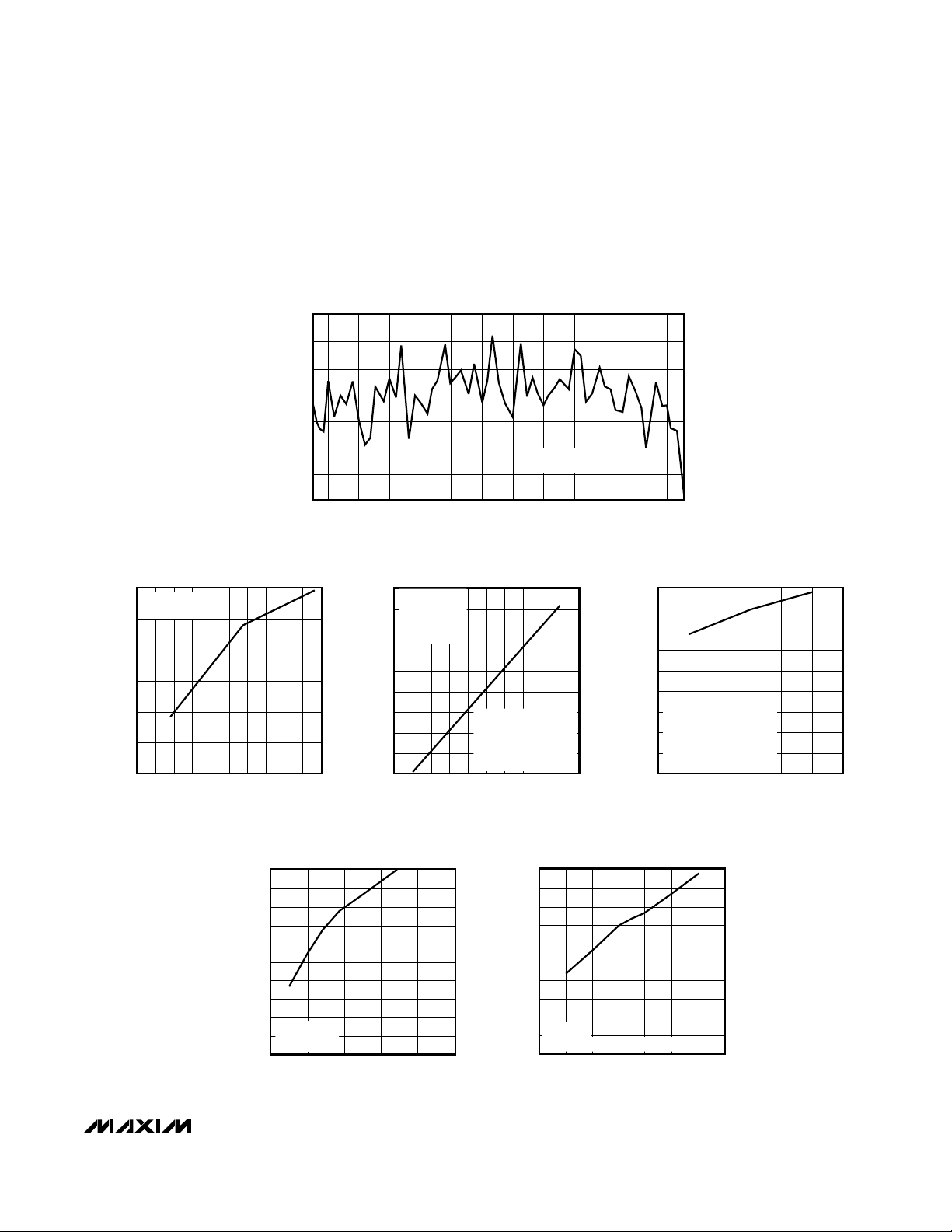
6-Bit Quadrature Digitizer
____________________________Typical Operating Characteristics (continued)
(VCC= 5V, TA = +25°C, unless otherwise noted.)
VREF (PIN 88) VOLTAGE vs.
SUPPLY VOLTAGE
1.215
MAX2101
1.214
1.213
VREF (V)
1.212
1.211
1.210
4.75 4.85 4.95 5.05 5.15 5.25
VCC (V)
MAX2101 TOC 04
VPTAT (PIN 97) vs.
TEMPERATURE
1.4
1.3
1.2
1.1
VPTAT (V)
1.0
0.9
0.8
0 10203040506070
TEMPERATURE (°C)
PWR (PINS 85, 96) VOLTAGE vs.
BASEBAND AMPLITUDE
4.5
4.0
3.5
3.0
2.5
2.0
PWR (V)
1.5
1.0
0.5
0
TA = +25°C
0 0.4 0.6 0.8 1.0 1.2 1.4 1.6 1.8 2.00.2
BASEBAND AMPLITUDE (V)
TA = +70°C
MAX2101 TOC 05
MAX2101 TOC 07
VPTAT (PIN 97) VOLTAGE vs.
SUPPLY VOLTAGE
1.20
1.18
1.16
1.14
1.12
1.10
VPTAT (V)
1.08
1.06
1.04
1.02
1.00
4.75 4.85 4.95 5.05 5.15 5.25
VCC (V)
MAX2101 TOC 06
DIFFERENTIAL LINEARITY vs.
ADC CODE
100m
50m
0
-50m
-100m
ADJ CODE DELTA ERROR (LSB)
-150m
5 1015202530354045505560
ADJ CODE DELTA ERROR (LSB) vs. CODE
CODE
DNL = 0.173 LSB
MAX2101 TOC 10
6 _______________________________________________________________________________________
6-Bit Quadrature Digitizer
____________________________Typical Operating Characteristics (continued)
(VCC= 5V, TA = +25°C, unless otherwise noted.)
INTEGRAL NONLINEARITY vs.
ADC CODE
RF SIGNAL PATH GAIN vs.
AGC (PIN 93) VOLTAGE
60
fLO = 624MHz
= 5.1MHz
f
BB
50
40
30
GAIN (dB)
20
10
0
1.0 1.2 1.4 1.6 1.8 2.0 2.2 2.4 2.6 2.8 3.0
VAGC (V)
100m
50m
0
-50m
ERROR (LSB)
-100m
-150m
ADC ERROR (LSB) vs. CODE
INL = 0.15 LSB
5 1015202530354045505560
CODE
INPUT IP3 vs.
IF POWER
9
8
7
6
5
4
IIP3 (dBm)
3
2
1
0
MAX2101-TOC 12
10
fLO = 668MHz
f
= 5.1MHz
5
BB1
f
= 6.1MHz
BB2
0
fC = 10MHz
-5
-10
-15
IIP3 (dBm)
-20
-25
-30
-35
-55 -50 -45 -40 -35 -30 -25 -20 -15 -10 -5
P
= P
(BB1)
@ P
(FSIN)
P
= P
(BB1)
@ P
(FSIN)
IF POWER (dBm)
= -16dBm
(BB2)
= -10dBm
= -56dBm
(BB2)
= -50dBm
MAX2101-TOC 13
MAX2101 TOC 11
INPUT IP3 vs.
FILTER CUTOFF FREQUENCY
fLO = 464MHz or 668MHz
f
= 5.1MHz
BB1
f
= 6.1MHz
BB2
P
= P
(BB1)
P
(FSIN)
5 101520253035
= -16dBm
(BB2)
= -10dBm
CUTOFF FREQUENCY (MHz)
MAX2101
MAX2101-TOC 14
NOISE FIGURE vs.
IF INPUT POWER
30
28
26
24
22
20
18
NF (dB) (DSB)
16
14
fLO = 624MHz
12
f
= 10MHz
BB
10
-55 -50 -45 -40 -35 -30
IF POWER (dBm)
MAX2101-TOC 15
2.0
1.9
1.8
1.7
1.6
1.5
IFIN VSWR
1.4
1.3
1.2
1.1
1.0
IFIN (PIN 90) VSWR vs.
FREQUENCY
RS = 50Ω
(PIN 91) I
200 300 400 500 600 700 800 900
AC TERMINATED IN 25Ω
FINB
FREQUENCY (MHz)
MAX2101-TOC 16
_______________________________________________________________________________________
7
6-Bit Quadrature Digitizer
______________________________________________________________Pin Description
PIN
1, 9,
12, 13,
18, 19,
63, 67,
82, 83,
89, 92,
MAX2101
98, 99
2 VGNDQ Q Channel Baseband Ground
3 BBINQ
4 FTUNEQ
5 OFFQ
6 BBOUTQ
7 BBOUTQB
8 VCCQ Q Channel Baseband +5V Supply
10 VGNDP Prescaler Ground
11 VCCP Prescaler +5V Supply
14 TNKB Oscillator Resonator Port
15 VCC2 Oscillator +5V Supply
16 VGND2 Oscillator Ground
17 TNKA Oscillator Resonator Port
20, 21 VGNDAD A/D Converter Ground
22, 59 VSUBAD A/D Converter Substrate
23 VCOPRE Divide-by-16 Prescaler Output
24 VCOPREB
25, 29,
38, 40,
44, 52
26 VGNDO Digital Output Ground
27 D5Q Q Channel Data Output, bit 5 (MSB)
28 D4Q Q Channel Data Output, bit 4
30, 37,
43, 51,55VGNDO Digital Output Ground
31 D3Q Q Channel Data Output, bit 3
32 D2Q Q Channel Data Output, bit 2
33, 48 VCCD Digital Logic +5V Supply
34, 47 VGNDD Digital Logic Ground
NAME FUNCTION
GND Ground
Q Channel Baseband Amplifier,
External Input
Q Channel Filter Cutoff
Frequency Control
Q Channel Baseband Amplifier
Offset Adjust
Q Channel Baseband Amplifier
Output
Q Channel Baseband Amplifier
Inverted Output
Divide-by-16 Prescaler
Complementary Output
VCCO Digital Output +5V Supply
PIN
35 D1Q Q Channel Data Output, bit 1
36 D0Q Q Channel Data Output, bit 0 (LSB)
39 RCLK
41 DCLKB Data Clock Complementary Output
42 DCLK Data Clock Output
45 D0I I Channel Data Output, bit 0 (LSB)
46 D1I I Channel Data Output, bit 1
49 D2I I Channel Data Output, bit 2
50 D3I I Channel Data Output, bit 3
53 D4I I Channel Data Output, bit 4
54 D5I I Channel Data Output, bit 5 (MSB)
56 BINEN Binary Enable
57 S2
58 S1
60, 61 VCCAD A/D Converter +5V Supply
62 S0
64 VCCC Clock Buffer +5V Supply
65 MCLK Master Clock
66 VGNDC Clock Buffer Ground
68 ENOPB Offset Correction/Enable Correction
69 CQB
70 CQ
71 CI
72 CIB
73 VCCI I Channel Baseband +5V Supply
74 BBOUTIB
75 BBOUTI I Channel Baseband Amplifier Output
76 OFFI
77 FTUNEI
NAME FUNCTION
Reference Clock, divide by six from
master clock (MCLK)
Programmable Sample Rate
Control Input, bit 2 (MSB)
Programmable Sample Rate
Control Input, bit 1
Programmable Sample Rate
Control Input, bit 0 (LSB)
Inverting Input Q Channel Offset
Correction
Noninverting Input Q Channel
Offset Correction
Noninverting Input I Channel Offset
Correction
Noninverting Input I Channel Offset
Correction
I Channel Baseband Amplifier
Inverted Output
I Channel Baseband Amplifier
Offset Adjust
I Channel Filter Cutoff Frequency
Control
8 _______________________________________________________________________________________

6-Bit Quadrature Digitizer
_______Pin Description (continued)
PIN NAME FUNCTION
78 BBINI
79 VGNDI I Channel Baseband Ground
80 VREFIN
81 MIXOUTI I Channel Mixer Output
84 VSUBRF RF Demodulator Substrate
85 PWRI I Channel Power Indicator
86 2R5 2x VREF Output
87 VCCIF IF Signal Processing +5V Supply
88 VREF
90 IFIN IF Amplifier Noninverting Input
91 IFINB IF Amplifier Inverting Input
93 AGC Automatic Gain Control Input
94 VGNDIF IF Signal-Processing Ground
95 FLTRSEL Baseband Signal Path Select
96 PWRQ Q Channel Power Indicator
97 VPTAT PTAT Reference Voltage Output
100 MIXOUTQ Q Channel Mixer Output
I Channel Baseband Amplifier,
External Input
High Impedance, connect to VREF
(pin 88)
Bandgap Reference Voltage
Output
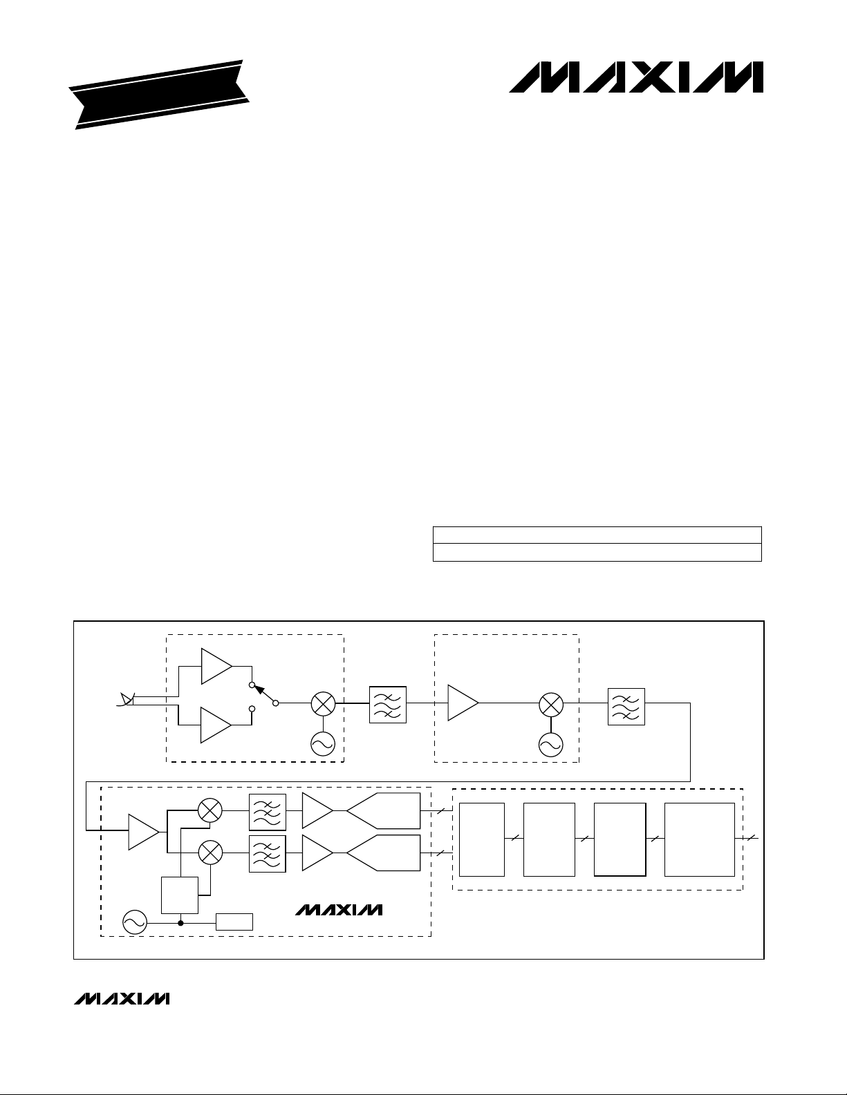
______________Detailed Description
The MAX2101 6-bit quadrature digitizer solves one of
the most challenging problems of high dynamic range
digital-receiver design by combining quadrature
demodulation and analog-to-digital (A/D) conversion in
a single device. The MAX2101’s unique RF-to-Bits
function bridges the gap between RF downconverters
and CMOS digital signal processors (DSPs). Figure 1
is a simplified connection diagram.
The MAX2101 accepts input signals from 400MHz to
700MHz and applies gain depending on the input
amplitude. The signal is then split and downconverted
to baseband by two mixers, which are driven by two
local oscillator (LO) signals in quadrature. An internal
voltage-controlled oscillator (VCO) feeds the two LOs.
Each baseband is filtered by an internal 5th-order
Butterworth lowpass filter. The on-board lowpass filters
have an externally variable bandwidth of 10MHz to
30MHz. Each baseband is then converted by a 6-bit
analog-to-digital converter (ADC). The conversion result
is stored in a register and is output using the data
clock. See Figure 2 for the relation between baseband
signal, sample and data clock, and digitized data. The
external master clock is internally divided by six and is
available at RCLK for external system functions, frequency synthesizers, etc. See Figures 3 and 4 for functional diagrams.
IF Input Port (IFIN,
The MAX2101 provides a balanced IF input. The inputs
are self-biasing, so the input signals should be AC terminated, depending on system requirements. To minimize
noise, the unused input should be AC terminated with
25Ω. To minimize distortion, AC terminate the unused
input with a 50Ω resistor.
IFINB
VCO Resonator Tank Ports
(TNKA, TNKB) and Prescaler
The MAX2101 integrates a negative impedance oscillator with balanced inputs. Use a parallel tank network,
as shown in Figure 5. The phase-noise performance of
the oscillator near the carrier is dominated by the resonant network. The resonant inductor must have a sufficiently high Q and a self-resonant frequency (SRF) that
is more than twice the intended LO frequency. Be sure
to minimize parasitic elements surrounding the tank
network by using proper layout techniques. See the
Applications Information
The VCO prescaler output provides phase-lock loop
capability for controlling the VCO frequency. The
prescaler generates the VCO frequency divided by 16.
As a result, the prescaler delivers a 25MHz to
43.75MHz signal over the VCO operating frequency
range of 400MHz to 700MHz. The differential outputs
should have equivalent termination.
section.
MAX2101
)
_______________________________________________________________________________________ 9

6-Bit Quadrature Digitizer
V
CC
1k
MAX2101
2k
IF INPUT SIGNAL
400MHz to
700MHz
1
0.01µF
5.6k
0.01µF
REFERENCE FREQUENCY
⁄2
MAX407
4k
2k
PHASE-LOCKED LOOP
V
CC
2.2k
V
CC
INPUT
GAIN
ADJUST
0.01µF
FILTER
TUNE
20k
20k
20k
0.01µF
0.1µF
1
⁄2
MAX407
50Ω
0.22µF
20k
1000pF
0.1µF
0.22µF
0.22µF
0.22µF
50Ω
25Ω
0.01µF
50Ω
68
ENOPB FLTRSEL
71
CI
72
CIB
76
OFFI
77
FTUNEI
93
AGC
90
IFIN
91
IFINB
88
VREF
97
VPTAT
4
FTUNEQ
80
VREFIN
MAX2101
5
OFFQ
69
CQB
70
CQ
23
VCOPRE
24
VCOPREB
PHASE
DETECTOR
BINEN
MCLK
PWRI
D5I
D4I
D3I
D2I
D1I
D0I
DCLK
DCLKB
D5Q
D4Q
D3Q
D2Q
D1Q
D0Q
PWRQ
RCLK
TNKA
TNKB
95
56
62
S0
58
S1
57
S2
0.1µF
65
I CHANNEL
85
54
53
50
49
46
45
42
41
27
28
31
32
35
36
96
39
17
14
POWER-DETECT
OUTPUT
10k
0.01µF
PARALLEL
RESONANT
TANK
(FIGURE 5)
LOOP
FILTER
50Ω
I CHANNEL DATA OUTPUT
Q CHANNEL DATA OUTPUT
10k
MASTER
CLOCK
INPUT
(60MHz)
DATA
CLOCK
0.01µF
Q CHANNEL
POWER-DETECT
OUTPUT
Figure 1. Typical Connection Diagram
10 ______________________________________________________________________________________

6-Bit Quadrature Digitizer
OUT
N
t
APERTURE
t
PCQ
t
SKEW
ANALOG
INPUT
DATA
CLOCK
DATA
NOTE: DATA IS VALID ON
THE RISING EDGE OF DCLK.
Figure 2. Baseband Signal, Sample/Data Clock, and Digitized Data Timing
N + 1
t
PC
DATA VALID N-1
MAX2101
N + 2
DATA VALID N
(PIN 90)
IFINB
(PIN 91)
TNKA
(PIN 17)
TNKB
(PIN 14)
IFIN
40dB to 0dB
400MHz to 700MHz
400MHz to 700MHz
AGC
(PIN 93)
AGC
0°
90°
0: INTERNAL
1: EXTERNAL
DIV-16
6dB
0dB
0dB
6dB
FLTRSEL
(PIN 95)
MIXOUTI
(PIN 81)
FTUNEI
(PIN 77)
LPF
10MHz to 30MHz
LPF
10MHz to 30MHz
FTUNEQ
(PIN 4)
MIXOUTQ
(PIN 100)
VCOPRE
(PIN 23)
VCOPREB
(PIN 24)
BBINI
(PIN 78)
EN
EN
BBINQ
(PIN 3)
1
2:1
0
MUX
0
⁄
1
GND: ENABLE
VCC: DISABLE
0
⁄1
2:1
0
MUX
1
ENOPB
(PIN 68)
OFFI
(PIN 76)
OFFQ
(PIN 5)
CIB
(PIN 72)
EN
EN
CQB
(PIN 69)
150k
150k
150k
150k
CI
(PIN 71)
2
2
CQ
(PIN 70)
BBOUTI
(PIN 75)
BBOUTIB
(PIN 74)
1.5V
p-p
(DIFFERENTIAL)
BASEBAND
CHANNEL I
PWRI
(PIN 85)
PWRQ
(PIN 96)
1.5V
p-p
(DIFFERENTIAL)
BASEBAND
CHANNEL Q
BBOUTQ
(PIN 6)
BBOUTQB
(PIN 7)
Figure 3. Functional Diagram—MAX2101 RF Front-End Section
______________________________________________________________________________________ 11

6-Bit Quadrature Digitizer
REFERENCE
AMPLIFIER
FULL-SCALE/2
–
COMMON
BASEBAND
CHANNEL I
MODE
+
ADC
VREF
6
MAX2101
VREF
(PIN 88)
SAMPLE-RATE
BANDGAP
REFERENCE
BASEBAND
CHANNEL Q
VPTAT
(PIN 97)
ADC
6
3
ADJUST
DIV 6
S0-S2
DATA
BUFFER 6
B/2
D0I-D5I
DCLK
(PIN 42)
DCLKB
(PIN 41)
MCLK
(PIN 65)
RCLK
(PIN 39)
BINEN
(PIN 56)
COMMON
MODE
FULL-SCALE/2
REFERENCE
AMPLIFIER
VREF
Figure 4. Functional Diagram—MAX2101 ADCs and Supporting Sections
Filter Tuning
The MAX2101 integrates two 5th-order Butterworth lowpass filters for anti-alias filtering of the baseband signal. One filter exists for each of the I and Q channels.
The filters’ cutoff frequency is set by driving the FTUNE
pins, pin 77 (I channel) and pin 4 (Q channel). The user
sets the I/Q channel filters independently. Figure 6
shows a typical transfer curve of a filter’s cutoff frequency versus FTUNE voltage.
The MAX2101’s anti-aliasing filtering function provides
superior channel-to-channel matching compared to a
discrete implementation. The filters are realized using a
gyrator topology, which inherently has a strong temperature dependency. The temperature dependency of the
filters must be compensated to achieve a consistent filter response over ambient temperature. This compensation is easily summed with the user-supplied filter
tune signal, with the techniques discussed for both current-drive and voltage-drive implementations later in
this section. Figure 7 shows a typical characteristic of
the FTUNE signal required to provide a constant filter
cutoff frequency over temperature.
Figure 5. Typical Parallel Resonant Network
FROM
PLL
FILTER
C
VAR
2pF to 10pF
R
BUF
10k
R
BUF
10k
C
FLTR
0.1µF
DATA
BUFFER
6
B/2
V+
R
CHOKE
1k
C
VAR
2pF to 10pF
C
470pF
C
SH
3pF to 12pF
C
470pF
D0Q-D5Q
C
14
TNKB
MAX2101
L
RES
8nH
17
TNKA
C
12 ______________________________________________________________________________________

6-Bit Quadrature Digitizer
MAX2101
FILTER CUTOFF FREQUENCY
vs. FTUNE
30
TA = +25°C
25
MAX2101 TOC Fig 6
2.00
1.95
FILTER CUTOFF FREQUENCY
TEMPERATURE DEPENDENCE
fC = 15MHz
MAX2101 TOC Fig. 7
20
15
CUTOFF FREQUENCY (MHz)
10
5
1.0 1.2 1.4 1.6 1.8 2.0 2.2 2.4 2.6 2.8
FTUNE (V)
Figure 6. Typical Filter Cutoff Frequency vs. FTUNE Input
Voltage
The MAX2101 provides temperature-compensated bias
voltages that, when scaled and summed with the usersupplied filter-control signal, provide the necessary
compensation for the filters. The filter-control signal can
originate in one of two forms: an analog current, or an
analog voltage. The temperature compensation signal
will be added to the control signal as discussed below.
Voltage Drive
A suggested technique of filter drive uses a voltage
source, such as a voltage output DAC. The temperature compensation signals, VPTAT and VREF, are shifted and scaled, then summed with the control voltage,
and the sum is applied to the FTUNE inputs. See Figure
8 for a possible implementation.
The transfer function for Figure 8’s voltage drive configuration can be evaluated as follows:
R
VV
=+ −
TC REF
VV
FTUNE SET
=+ −
F
(V V )
REF PTAT
R
TC
R
F
R
TC
(V V )
REF PTAT
1.90
1.85
FTUNE (V)
1.80
1.75
1.70
Figure 7. Typical Filter Cutoff Frequency Temperature
Dependence
20 40 100
0 140
TEMPERATURE (°C)
80
60
120
Current Drive
An alternate form of filter drive uses a current source,
such as a current-output DAC. The current is transformed to the appropriate voltage via a transresistance
network, which will drive the FTUNE input(s). The temperature compensation signals, VPTAT and VREF, are
shifted and scaled, transformed to current, added to
the user-supplied current, and the sum is transformed
back into the temperature compensated control voltage
(Figure 9).
Amplifier U1A generates a shifted reference signal,
VTC. VTCis transformed into a current through the
resistor RTC. RTCalso scales this signal such that,
when compared to the feedback resistor RF, the proper
temperature dependence is added to the user-supplied
filter control current I
to compensate for the TC of
SET
the filter.
The expression for the final filter tune signal is
expressed as:
R
V I (R )
FTUNE SET F
=+ −
F
(V V )
REF PTAT
R
TC
Thus, the user-supplied signal V
, which is character-
SET
ized by a very small (ideally 0) temperature coefficient,
will be summed with a small signal (|V
200mV) whose temperature dependence compensates
REF
- V
PTAT
|
for the filter’s TC.
______________________________________________________________________________________ 13
≤

6-Bit Quadrature Digitizer
VREF
(PIN 88)
R
R
R
DACA
VSET
MAX2101
R
2.2k
R
5.6k
S
1
⁄4
TC
MAX418
DACB
R
F
4.7k
(PIN 88)
VREF
VSET
VTC
R
R
VREF
(PIN 88)
VPTAT
(PIN 97)
Figure 8. Independent Filter Tune Control Using Two Voltage-Output DACs
R
R
1
⁄4
MAX418
R
1
⁄4
MAX418
27Ω
27Ω
0.01µF
0.01µF
FTUNEI
(PIN 77)
FTUNELQ
(PIN 4)
R = 33kΩ, 1%
= 5V
V
CC
R
F
27Ω
27Ω
VPTAT
(PIN 97)
33k, 1%
I
SET
0.3mA to 1mA
33k, 1%
1
⁄2
DAC
VTC
RTC
5k,
1%
4k
1
⁄2
MAX407
MAX407
VREF
(PIN 88)
33k, 1%
33k, 1%
VCC = 5V
Figure 9. Filter Tune Control Using a Single Current-Output DAC
14 ______________________________________________________________________________________
(Q CHANNEL, PIN 4)
0.01µF
FTUNE
(I CHANNEL, PIN 77)
0.01µF

6-Bit Quadrature Digitizer
Filter Temperature Compensation
In both techniques discussed above, the ratio RF/RTCdetermines the compensation required to produce a
filter response with 0TC. As noted in the VPTAT vs.
Temperature graph in the
this ratio should be set at 0.8.
Typical Operating Characteristics
,
Baseband Offset Correction
The MAX2101 integrates a high level of RF signal processing, and applies substantial gain from the IF inputs
to the baseband signals applied to the ADC. Offset in
the signal path can seriously decrease the component’s dynamic range, and variation in offset between I
and Q channels can seriously degrade overall receiver
performance. Several circuit design techniques are
used to minimize offset within the chip. However, two
characteristics of the component contribute to offset in
the signal path.
The off-chip tank network for the VCO resonates the LO
frequency with a relatively large amplitude. If the LO
couples into the IF input, the coupled LO will mix down
to a DC value, which depends on the AGC setting. This
DC signal manifests itself as an offset in the baseband
signal. The second source of offset is the active lowpass anti-aliasing filters. This offset depends on the
cutoff frequency. These two elements represent the
major contributors to DC offset in the signal path.
Offset Adjust Pins OFFI, OFFQ
The MAX2101 offers an offset adjust pin for each of the
I and Q channels, labeled OFFI and OFFQ, respectively. The offset adjust input exhibits an adjustment range
that is sufficient to correct for the errors mentioned
above. The polarity of the OFF_ input is such that a
positive change of the OFF_ voltage results in a negative transition in the baseband signal, BBOUT_. The offset adjust range compensates for up to 5LSBs of offset.
A feedback-controlled, offset-correction network can
be realized that will null any offset detected in the baseband signal applied to the ADCs. The differential baseband signal is sampled at the input to the ADC and
integrated over a sufficiently large period of time (determined by the minimum frequency of the baseband signal), extracting the offset signal. This error signal is
internally applied to the OFF_ input, completing the
feedback loop. The MAX2101 integrates the op amps
and 150kΩ pickoff resistors of the offset correction network. Figure 10 shows a simplified schematic diagram
of the network. Simply connect the appropriate capacitors as shown in Figure 11.
The network in Figure 11 is a lowpass filter with a 5Hz
cutoff frequency. The user can tailor the cutoff frequency
by choosing the appropriate value of capacitance,
according to the following relation:
C
=
where:
C = integrator capacitance
for cutoff frequency
Frequency components of the baseband signal near or
below the cutoff frequency will interfere with the operation of this network. Fortunately, the compressed and
encoded nature of baseband signals at this stage of
the signal chain in typical applications will insure minimal low-frequency components. Hence, this technique
will eliminate all offsets, independent of AGC setting, filter cutoff frequency, or changes in ambient temperature.
Pin 68, ENOPB, is normally connected to ground.
Pulling ENOPB to V
opening the servo loop, and disabling offset correction.
The baseband pins (6, 7, 74, 75) should be left unconnected, or buffered with a high-impedance load (resistive load greater than 10kΩ and capacitive load less
than 3pF).
1
2 f (150k )
π
O
Ω
CC
disables the op amps, thus
Sample Clock Generation
The master sample clock (MCLK) input for the
MAX2101 is typically driven by a low-noise, low-drift
crystal oscillator. The signal should be between 0dBm
and +10dBm, and must be AC coupled to the MCLK
input. This signal is buffered and divided according to
the programmable sample-rate prescaler (PSRP). The
actual sample rates are binary weighted divisors of the
MCLK frequency. Program the sample rates with pins
S0, S1, and S2, as shown in Table 1.
Table 1. Sample-Rate Control
S2 S1 S0 Sample Rate Description
000 fc/1 Full Sample Rate
001 fc/2 Div–2 Sample Rate
010 fc/4 Div–4 Sample Rate
011 fc/8 Div–8 Sample Rate
100 fc/8 Div–8 Sample Rate
101 fc/16 Div–16 Sample Rate
110 fc/32 Div–32 Sample Rate
111 fc/64 Div–64 Sample Rate
Note: The inputs S0, S1, and S2 are not latched.
MAX2101
______________________________________________________________________________________ 15

6-Bit Quadrature Digitizer
71
72
CIB CI
76
OFFI
68
MAX2101
Figure 10. Offset Correction Network Figure 11. Offset Correction
ENOPB
5
OFFQ
CQB CQ
69
150k
150k
MAX2101
150k
150k
70
BBOUTI
BBOUTIB
BBOUTQB
BBOUTQ
75
74
7
6
220nF
5
MAX2101
OFFIOFFQ
CIB
CQB
ENOPB
CQ
76
220nF
72
71
CI
70
69
68
220nF 220nF
Digital Signal Interfacing
The single-ended, LS-TTL compatible data outputs
from the ADCs are clocked out with respect to the rising edge of the data clock (DCLK). The output drivers
provide sufficient logic levels at speeds up to 60Mbps
into a fanout of 1 with a total load capacitance of 15pF.
All data outputs should have approximately equivalent
loading to ensure proper setup and hold timing.
The data clock outputs are also LS-TTL compatible and
provide a signal to latch the data at rates up to
60Mbps. The outputs are differential to minimize the
harmonic energy that might feed back into the LO or IF
inputs. The balanced outputs should have equivalent
termination to minimize unwanted EMI.
Select either binary or twos-complement output with the
binary enable (BINEN) pin. A logic high will select offset
binary, and a logic low will select a twos-complement
format.
Input Termination Network
The MAX2101 accepts as an input a narrow band IF
whose center frequency is located somewhere in the UHF
range, between 400MHz and 700MHz. The MAX2101
comprises a significant part of a receiver chain characterized by extremely high dynamic range coupled with
demanding intermodulation requirements. As such, it is
imperative to provide proper input termination to the
MAX2101, to minimize effective VSWR and noise figure at
this stage of the system RF signal processing chain.
The input of the MAX2101 is designed to deliver a
VSWR less than 2:1 over the 400MHz to 700MHz range.
The equivalent input network of the input pins IFIN and
IFINB is discussed and illustrated below. However,
standard narrow-band impedance matching techniques can be used to improve on this VSWR for the
intended IF of the system.
Equivalent Input Circuitry
The MAX2101’s input amplifier is designed to provide a
controlled input impedance, provide gain for the signal
path, and provide for the component’s minimum noise
figure. The amplifier uses a feedback topology to provide gain that is insensitive to input frequency, in addition to delivering constant input impedance. Figure 12
illustrates the amplifier’s input portion.
Ideally, the input amplifier will be designed to match to
an anticipated source impedance of 50Ω. The resistive
portion of the input impedance at pin IFIN can be
approximated as follows:
Rr
+
IN
FE
=
(1 A )
+
V
R
where rEis the dynamic resistance at Q3’s emitter, and
AVis the open-loop gain of the differential-pair amplifier
stage.
The amplifier can be designed so the frequency
response does not appreciably affect the input impedance. Details of the amplifier are left out for simplicity.
Figure 12 shows how several parasitic elements contribute to the input impedance over the frequencies of
interest. C
represents the parasitic capacitance
PAD
associated with the bond pad and input metallization.
16 ______________________________________________________________________________________

6-Bit Quadrature Digitizer
V
CC
MAX2101
R
I
IFIN
(PIN 90)
L
BW
C
PAD
R
F
Q1 Q2
R
Figure 12. Equivalent Input Network
At frequencies of interest, C
will add a small phase
PAD
error to the impedance term. The inductance LBWmodels the bond wire and lead frame in series with the
input amplifier. This inductor represents a significant
portion of the input impedance, and will contribute the
majority of the variation in input impedance as the input
frequency is swept from 400MHz to 700MHz. These
variables combine to produce an actual input impedance versus frequency (Figure 13).
As a result, it is challenging to achieve an extremely low
VSWR for the input of a monolithic amplifier, especially
over a wide range of frequencies. The MAX2101 provides
a VSWR less than 2:1, and delivers this performance over
the wide range of anticipated IFs currently considered.
Fortunately, for DBS, TVRO, and related applications, the
UHF IF is relatively narrow band, allowing the use of standard techniques for narrow-band impedance matching.
Narrow-Band Match
Many references cover narrow-band matching techniques. The match network synthesis is simplified by
assuming the impedance of the source driving the
MAX2101’s IFIN port is positive, real, and equal to 50Ω.
For a given IF, you can simply use a Smith chart to
“map” an impedance to the intended source resistance. Using a two-element matching network, you can
choose the element next to the input (CSHin Figure 14)
to translate the real portion of the impedance to match
the source resistance. The second element (L
SER
in
Figure 14) cancels the reactive component of the network (including the effect of CSH), resulting in a real,
matched input impedance that provides maximum
R
I
Q4Q3
R
F
R
E
E
L
BW
C
PAD
IFINB
(PIN 91)
IFIN (PIN 90) INPUT IMPEDENCE vs.
FREQUENCY
80
60
40
(Ω)
20
IN
Z
0
-20
-40
300 400 700
200 900
TA = +25°C
= 5V
V
CC
= 50Ω
R
S
IFINB (PIN 91) AC TERMINATED IN 25Ω
500
FREQUENCY (MHz)
600
RE (ZIN)
IM (ZIN)
800
Figure 13. Typical MAX2101 IFIN ZINvs. Frequency (Zs = 50)
power transfer. The transformation uses only reactive
elements so that no additional resistive thermal noise is
added, which would degrade the noise figure.
Figure 14 shows the resulting impedance matching network. The incident signal is AC coupled by C
and CSHare the matching elements. CSHincludes
board layout capacitance. The values of these ele-
MAX2101 TOC Fig. 15
. L
C
SER
______________________________________________________________________________________ 17

6-Bit Quadrature Digitizer
C
C
10nF
= 600MHz)
(f
S
R
S
50Ω
V
S
(-47dBm to -7dBm)
MAX2101
Figure 14. Example of Input Network to Minimize VSWR and Noise Figure
ments were calculated assuming a 600MHz source frequency. Capacitor C
for the complementary input IFINB. Resistor R
vides superior noise figure performance by optimizing
the tradeoff between thermal induced noise and the
gain of the input amplifier. This network also provides
ancillary rejection of out-of-band energy, improving the
receiver noise figure and resulting SNR. The topology
shown above produces a VSWR less than 1.7:1 over
the intended UHF band. Do not DC couple the inputs to
ground, as this would result in saturation of the input
stage.
More elaborate matching networks can be designed
depending on the need of the receiver system.
__________Applications Information
Voltage-Controlled Oscillator Equivalent
Input Network and Resonator Issues
The MAX2101 performs the quadrature demodulation
and digitizing functions within a digital receiver system.
A vital component of the quadrature detection function
is the generation of a local oscillator (LO) frequency.
This signal is typically generated by a VCO controlled
by a phase-locked loop. The VCO topology normally
used for high dynamic range receivers is the negative
resistance amplifier and resonator, due to superior
phase-noise performance. The MAX2101 provides the
negative resistance amplifier on-chip, and can be easily interfaced with an off-chip resonant network.
The MAX2101’s VCO amplifier uses a differential topology for several reasons. The differential interface with
provides an AC termination
TERM
TERM
pro-
L
8nH
SER
C
R
TERM
25Ω
TERM
10nF
C
1pF
SH
90
IFIN
MAX2101
91
IFINB
the resonator network provides superior rejection of
spurious signals that might otherwise add to or distort
the resulting LO. The differential interface minimizes the
effect of parasitic package-related elements that affect
the resonant frequency and the loaded Q of the network. The differential-drive network minimizes secondharmonic distortion that might create undesirable
mixing products within the signal chain.
Figure 15 shows the simplified input network of the
negative impedance amplifier, configured as a Wilson
oscillator. The amplifier is a simple differential emitter
coupled pair with emitter degeneration for controlled
open-loop gain. The positive feedback necessary to
create the negative input impedance is performed with
the feedback capacitors, C
, and the coupling capaci-
F
tors, CC. The capacitors ensure operation over the
intended 400MHz to 700MHz spectrum, and add minimal noise to the system. RB1provides a proper bias
voltage for the capacitors (partially constructed with
voltage-dependent pn junctions) and provides for DC
interface with a shunting resonant inductor. Note that
biasing networks are simplified for brevity.
The MAX2101’s negative impedance amplifier expects
a parallel resonant network. Figure 5 shows an example
of a tunable resonant network. The resonator is driven
from the phase-locked loop filter output, as noted. The
loaded Q of the resonant network, and to a lesser
extent the absolute values of the resonant elements,
determine the VCO’s phase-noise performance. As a
result, take care during the design of the resonator to
maximize the loaded Q. To achieve the phase-noise
18 ______________________________________________________________________________________

6-Bit Quadrature Digitizer
V
CC
MAX2101
R
I
C
F
C
C
TNKA
(PIN 17)
R
B1
V
B1
Figure 15. Simplified Input Network for VCO Resonator Ports
R
B2
R
E
performance in the specification, the resonant network
should exhibit a loaded Q greater than 20.
The resonating inductor L
should exhibit as high a
RES
Q factor as is reasonably possible. The inductor’s selfresonant frequency (SRF) should be well in excess of
the intended frequencies of operation. An air-wound
design is a simple example of an inductor that would fit
these criteria.
A dual varactor topology is recommended for C
VAR
to
compensate for the large-signal amplitude incident
across the resonator ports. The dual varactor in the
arrangement shown in Figure 5 (to first order) allows
cancellation of capacitance modulation due to the large
signals, as the two diodes are driven in a complementary fashion by the LO signal. The dual varactor design
also allows use of devices with larger COvalues, simplifying device selection. The varactor should be driven
with a large reverse bias to increase the MAX2101’s
effective Q.
The resonant frequency is primarily determined by
CSH, which shunts the varactor diodes. CSHis trimmed
(selected) to determine the approximate tuning range
of the phase-locked loop. For applications relevant to
the MAX2101, this frequency range can cover the UHF
R
I
C
F
R
E
I
EE
C
C
TNKB
(PIN 14)
R
B2
R
B1
V
B2
spectrum from 400MHz to 700MHz. The varactor within
the loop will then determine the actual LO frequency
within a much narrower tuning range. Depending on
the expected tuning range variation, CSHcould be
made of a combination of fixed capacitance and
trimmed capacitance. This shunt capacitance will
increase the loaded Q of the resonator and lower the V
to F gain constant, improving the oscillator’s phasenoise performance.
The coupling capacitors CCcouple the variable capacitor network to the tank ports and resonating inductor.
These elements should be selected to present low
impedance (less than 1Ω) at the lowest expected operating frequency. These capacitors should also exhibit
low effective series resistance (ESR) to maintain a high
resonator-loaded Q. R
CHOKE
provides a DC bias for
the varactors, while ensuring a high impedance at the
intended operating frequency. The magnitude of the
choke network’s series impedance should be approximately 10 times the resonant inductor’s impedance at
the operating frequency. Resistors R
provide drive
BUF
for the varactor while ensuring adequate isolation
between the two differential resonator ports. C
combination with R
provides additional filtering of
BUF,
FLTR
, in
the drive signal from the loop.
______________________________________________________________________________________ 19

6-Bit Quadrature Digitizer
DBS System Application
A direct-broadcast satellite (DBS) receiver consists of
an antenna to receive the X/Ku band carrier from the
satellite, a low-noise block (LNB), an L-band downconverter, and a quadrature demodulator. The system
stages include a dual ADC, a matched filter, clock and
carrier recovery, error detection and correction, and
additional system-dependent DSP. See the
Application Circuit
MAX2101
The LNB provides polar demodulation (vertical and horizontal) and downconversion of the X/Ku band signals
to a first intermediate frequency (IF1) in the 950MHz to
2000MHz range. The L-band downconverter converts
IF1to a second IF (IF2) in the 400MHz to 700MHz
range. The MAX2101 performs the next stages as follows: 1) the quadrature demodulator converts IF2to
two baseband signals, I and Q; and 2) the dual ADCs
digitize the baseband signals, which are then
processed by the various digital blocks to compensate
for transmission distortion and to extract the digital
baseband data.
One interface that causes system designers trouble is
the quadrature demodulator to ADC interface. Power is
needed to drive the low-impedance interconnect
between these two functions. Additionally, this portion
of the signal path can introduce phase and amplitude
errors that complicate back-end error correction. The
integrated MAX2101 solves all of these design problems associated with DBS systems.
The MAX2101 combines bipolar technology with excellent RF and data-converter design to integrate the
quadrature demodulation and ADC functions. The
MAX2101 also includes an IF gain block, a VCO and
prescaler necessary to generate an accurate LO frequency, and fully integrated baseband anti-aliasing filters for both I and Q channels. By integrating several
functions supporting the quadrature demodulation and
A/D block, the MAX2101 replaces several components
and eliminates many board-level design and manufacturing problems.
on the first page of the data sheet.
Layout, Grounding, Bypassing
The MAX2101’s supply pins are separated to isolate
high-current digital noise spikes from sensitive RF and
analog sections. All ground potentials must be DC coupled, and resistive drops should contribute no more
than 50mV difference between the ground pins. A single-point analog ground (“star” ground point) should be
established at the ground supply connection to the PC
Typical
board, separate from the active circuitry. Three ground
planes should be established, connected at the star
ground point. The three ground planes should be dedicated as follows: analog and RF ground plane, digital
ground plane, and output ground plane. The various
ground pins should be connected to this star ground
network according to Table 2. The ground current
return path for all supplies should be low impedance at
frequencies of interest for each supply.
Table 2. Ground Plane Assignments
Ground Pin Pin Number Ground Plane
VGNDIF 94 analog
VGNDI 79 analog
VGNDQ 2 analog
VGND2 16 analog
VGNDAD 20, 21 analog
VGNDP 10 digital
VGNDC 66 digital
VGNDD 34, 47 digital
VGNDO 26, 30, 37, 43, 51, 55 output
For best performance, use printed circuit boards. Wirewrap boards are not recommended. Board layout
should ensure that digital and analog signal lines are
separated from each other. Do not run analog and digital (especially clock) lines parallel to one another, or
digital lines underneath the MAX2101 package.
The MAX2101 requires +5V ±5% for all supply pins.
Bypass the supply pins with high-quality 0.1µF and
0.001µF ceramic capacitors located as close to the
package as possible. The high-frequency supplies,
VCCIF and VCC2, both require an additional ceramic
surface-mount bypass capacitor nominally valued at
47pF. The baseband supplies (VCCI and VCCQ) need
additional filtering to ensure sufficient channel-to-channel isolation. Place a small-value resistor, such as 5Ω,
between the supply and the pins to create a single-pole
filter with the bypass capacitor. The DC IR drop across
the resistor should not exceed 150mV. Alternatively,
place an RF choke between the supply and the pins.
The SRF of the selected choke must be high enough to
block energy from the other baseband channel.
20 ______________________________________________________________________________________

6-Bit Quadrature Digitizer
____________________________________________________________Pin Configuration
TOP VIEW
GND
83
GND
82
MIXOUTI
81
80
VREFIN
79
VGNDI
78
BBINI
77
FTUNEI
76
OFFI
75
BBOUTI
74
BBOUTIB
73
VCCI
72
CIB
71
CI
70
CQ
69
CQB
68
ENOPB
67
GND
66
VGNDC
65
MCLK
64
VCCC
63
GND
S0
62
61
VCCAD
VCCAD
60
VSUBAD
59
S1
58
S2
57
56
BINEN
55
VGNDO
54
D5I
53
D4I
52
VCCO
51
VGNDO
GND
VGNDQ
BBINQ
FTUNEQ
OFFQ
BBOUTQ
BBOUTQB
VCCQ
GND
VGNDP
VCCP
GND
GND
TNKB
VCC2
VGND2
TNKA
GND
GND
VGNDAD
VGNDAD
VSUBAD
VCOPRE
VCOPREB
VCCO
VGNDO
D5Q
D4Q
VCCO
VGNDO
IFINB
GND
92
91
MAX2101
IFIN
90
GND
89
VREF
88
VCCIF
87
2R5
86
PWRI
85
VSUBRF
84
GND
99
GND
98
VPTAT
97
MIXOUTQ
100
1
2
3
4
5
6
7
8
9
10
11
12
13
14
15
16
17
18
19
20
21
22
23
24
25
26
27
28
29
30
PWRQ
96
VGNDIF
95
94
93
AGC
FLTRSEL
MAX2101
31
32
33
34
35
36
37
38
39
40
41
42
43
44
45
46
47
48
49
50
D3I
D3Q
D2Q
VCCD
VGNDD
D1Q
D0Q
VGNDO
VCCO
RCLK
VCCO
DCLKB
DCLK
VGNDO
VCCO
D1I
D0I
VGNDD
VCCD
D2I
MQFP
______________________________________________________________________________________ 21

6-Bit Quadrature Digitizer
________________________________________________________Package Information
ZD
MAX2101
PIN #1
A
BASE
PLANE
ZE
D
D1
D3
DIM
S
0.40
0.016 MIN.
R 0.012
0.005
E
DETAIL "A"
0° MIN.
E1
E3
DATUM
α
L
R 0.012
0.005 MIN.
PLANE
1.6
5°-16°
0.063
A
A
A1
A2
B
D
E
E1
E3
e
D1
D3
L
ZD
ZE
α
INCHES MILLIMETERS
MIN
0.110
0.010
0.100
0.009
0.904
0.667
0.547
0.783
0.026
MAX
0.134
–
0.120
0.015
0.923
0.687
0.555
0.486 REF
0.0256 BSC
0.742 REF 18.85 REF
0.023 REF
0.033 REF
0°
0.791
0.037
7°
MIN
2.79
0.25
2.55
0.22
22.95
16.95
13.90
12.35 REF
0.65 BSC
19.90
0.65
0.58 REF
0.83 REF
0°
MAX
3.40
–
3.05
0.38
23.45
17.45
14.10
20.10
0.95
7°
21-7003A
A1
A2
100-PIN MQFP
METRIC
Be
SEATING
PLANE
QUAD FLAT PACK
22 ______________________________________________________________________________________

6-Bit Quadrature Digitizer
MAX2101
______________________________________________________________________________________ 23

6-Bit Quadrature Digitizer
MAX2101
Maxim cannot assume responsibility for use of any circuitry other than circuitry entirely embodied in a Maxim product. No circuit patent licenses are
implied. Maxim reserves the right to change the circuitry and specifications without notice at any time.
24
__________________Maxim Integrated Products, 120 San Gabriel Drive, Sunnyvale, CA 94086 (408) 737-7600
© 1996 Maxim Integrated Products Printed USA is a registered trademark of Maxim Integrated Products.
 Loading...