

Page 1
19-0065; Rev 7; 12/05
+5V, RS-232 Transceivers
with 0.1µF External Capacitors
General Description
The MAX200–MAX209/MAX211/MAX213 transceivers
are designed for RS-232 and V.28 communication interfaces where Q12V supplies are not available. On-board
charge pumps convert the +5V input to the Q10V needed
for RS-232 output levels. The MAX201 and MAX209
operate from +5V and +12V, respectively, and contain a
+12V to -12V charge-pump voltage converter.
The MAX200–MAX209/MAX211/MAX213 drivers and
receivers meet all EIA/TIA-232E and CCITT V.28 specifications at a 20kbps data rate. The drivers maintain the
Q5V EIA/TIA-232E output signal levels at data rates in
excess of 120kbps when loaded in accordance with the
EIA/TIA-232E specification.
The 5FW shutdown mode of the MAX200, MAX205,
MAX206, and MAX211 conserves energy in battery-powered systems. The MAX213 has an active-low shutdown
and an active-high receiver enable control. Two receivers of the MAX213 are active, allowing the ring indicator
(RI) to be monitored easily using only 75FW power.
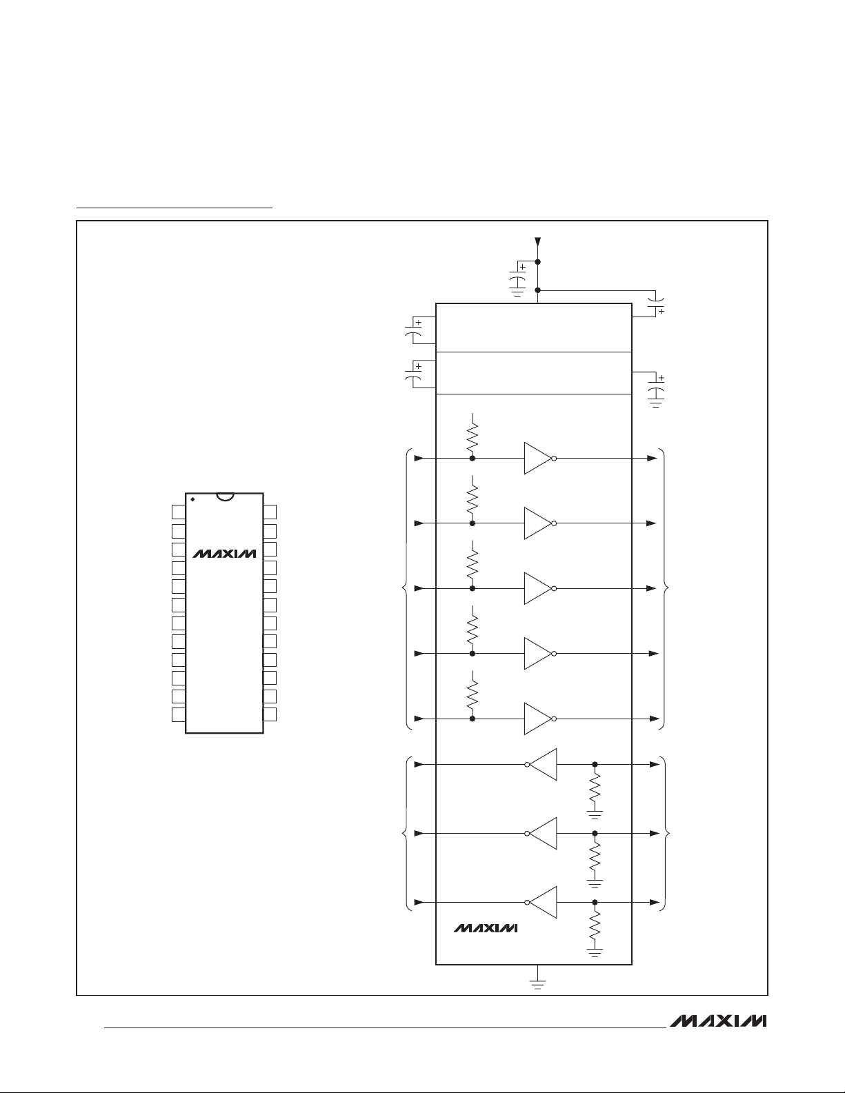
The MAX211 and MAX213 are available in a 28-pin, wide
small-outline (SO) package and a 28-pin shrink smalloutline (SSOP) package, which occupies only 40% of the
area of the SO. The MAX207 is now available in a 24-pin
SO package and a 24-pin SSOP. The MAX203 and
MAX205 use no external components and are recommended for applications with limited circuit board space.
Ordering Information appears at end of data sheet.
Selector Guide
Next-Generation Device Features
S For Low-Cost Applications:
MAX221E: ±15kV ESD-Protected, +5V, 1µA,
Single RS-232 Transceiver with AutoShutdown™
S For Low-Voltage and Space-Constrained Applications:
MAX3222E/MAX3232E/MAX3237E/MAX3241E/
MAX3246E: ±15kV ESD-Protected, Down
to 10nA, +3.0V to +5.5V, Up to 1Mbps, True
RS-232 Transceivers (MAX3246E Available in
UCSP™ Package)
S For Space-Constrained Applications:
MAX3228E/MAX3229E: ±15kV ESD-Protected,
+2.5V to +5.5V, RS-232 Transceivers in UCSP
S For Low-Voltage or Data Cable Applications:
MAX3380E/MAX3381E: +2.35V to +5.5V, 1µA,
2Tx/2Rx RS-232 Transceivers with ±15kV ESDProtected I/O and Logic Pins
S For Low-Power Applications:
MAX3224E–MAX3227E/MAX3244E/MAX3245E:
±15kV ESD-Protected, 1µA, 1Mbps,
+3.0V to +5.5V, RS-232 Transceivers with
AutoShutdown Plus™
Applications
Computers: Laptops, Palmtops, Notebooks
Battery-Powered Equipment
Handheld Equipment
MAX200–MAX209/MAX211/MAX213
PART
MAX200 +5 5 0 0 4 Yes/No
MAX201 +5 and +9.0 to +13.2 2 2 0 2 No/No
MAX202 +5 2 2 0 4 No/No
MAX203 +5 2 2 0 None No/No
MAX204 +5 4 0 0 4 No/No
MAX205 +5 5 5 0 None Yes/Yes
MAX206 +5 4 3 0 4 Yes/Yes
MAX207 +5 5 3 0 4 No/No
MAX208 +5 4 4 0 4 No/No
MAX209 +5 and +9.0 to +13.2 3 5 0 2 No/Yes
MAX211 +5 4 5 0 4 Yes/Yes
MAX213 +5 4 5 2 4 Yes/Yes
AutoShutdown, AutoShutdown Plus, and UCSP are trademarks of Maxim Integrated Products, Inc.
POWER-SUPPLY
VOLTAGE (V)
_______________________________________________________________ Maxim Integrated Products 1
NUMBER
OF RS-232
DRIVERS
NUMBER
OF RS-232
RECEIVERS
NUMBER OF
RECEIVERS
ACTIVE IN
SHUTDOWN
NUMBER OF
EXTERNAL
CAPACITORS
(0.1µF)
LOW-POWER
SHUTDOWN/TTL
THREE-STATE
For pricing, delivery, and ordering information, please contact Maxim Direct at 1-888-629-4642,
or visit Maxim’s website at www.maxim-ic.com.
Page 2
+5V, RS-232 Transceivers
with 0.1µF External Capacitors
ABSOLUTE MAXIMUM RATINGS
VCC ..........................................................................-0.3V to +6V
V+ .............................................................. (VCC - 0.3V) to +14V
V- ........................................................................... +0.3V to -14V
Input Voltages
TIN ......................................................... -0.3V to (VCC + 0.3V)
RIN ................................................................................... Q30V
Output Voltages
T
.................................................(V+ + 0.3V) to (V- - 0.3V)
OUT
R
..................................................... -0.3V to (VCC + 0.3V)
OUT
Short-Circuit Duration
T
.......................................................................Continuous
OUT
Continuous Power Dissipation (TA = +70NC)
14-Pin Plastic DIP (derate 10.00mW/NC above +70NC) ...800mW
16-Pin Plastic DIP (derate 10.53mW/NC above +70NC) ...842mW
16-Pin SO (derate 8.70mW/NC above +70NC) .............696mW
16-Pin Wide SO (derate 9.52mW/NC above +70NC) .... 762mW
16-Pin CERDIP (derate 10.00mW/NC above +70NC) ...800mW
20-Pin Plastic DIP (derate 11.11mW/NC above +70NC) ...889mW
Note 1: Maximum reflow temperature for the MAX203 and MAX205 is +225°C.
Stresses beyond those listed under “Absolute Maximum Ratings” may cause permanent damage to the device. These are stress ratings only, and functional
operation of the device at these or any other conditions beyond those indicated in the operational sections of the specifications is not implied. Exposure to absolute
maximum rating conditions for extended periods may affect device reliability.
20-Pin Wide SO (derate 10.00mW/NC above +70NC) .. 800mW
20-Pin CERDIP (derate 11.11mW/NC above +70NC) ...889mW
24-Pin Narrow Plastic DIP
(derate 13.33mW/NC above +70NC) ....................... 1067mW
24-Pin Wide Plastic DIP
(derate 9.09mW/NC above +70NC) ........................... 727mW
24-Pin Wide SO (derate 11.76mW/NC above +70NC) .. 941mW
24-Pin SSOP (derate 8.00mW/NC above +70NC) ......... 640mW
24-Pin CERDIP (derate 12.50mW/NC above +70NC) .1000mW
28-Pin Wide SO (derate 12.50mW/NC above +70NC) 1000mW
28-Pin SSOP (derate 9.52mW/NC above +70NC) ......... 762mW
Operating Temperature Ranges
MAX2_ _C_ _ ...................................................... 0NC to +70NC
MAX2_ _E_ _ ................................................... -40NC to +85NC
MAX2_ _ M_ _ ............................................... -55NC to +125NC
Storage Temperature Range ............................ -65NC to +160NC
Lead Temperature (soldering, 10s) (Note 1) ..................+300NC
ELECTRICAL CHARACTERISTICS
(MAX202/MAX204/MAX206/MAX208/MAX211/MAX213: VCC = +5V Q10%; MAX200/MAX203/MAX205/MAX207: VCC = +5V Q5%,
C1–C4 = 0.1FF; MAX201/MAX209: VCC = +5V Q10%, V+ = +9.0V to +13.2V, TA = T
PARAMETER CONDITIONS MIN TYP MAX UNITS
Output-Voltage Swing
MAX200–MAX209/MAX211/MAX213
VCC Power-Supply
Current
V+ Power-Supply Current No load
Shutdown Supply Current
Input Logic Threshold
Low
Input Logic Threshold
High
Logic Pullup Current T
RS-232 Input-Voltage
Operating Range
All transmitter outputs loaded with 3kI to ground Q5 Q8
MAX202, MAX203 8 15
No load, TA = +25NC
Figure 1, TA = +25NC
TIN, EN, SHDN, EN, SHDN
T
IN
EN, SHDN, EN, SHDN
= 0V 15 200
IN
MAX200, MAX204–MAX208, MAX211,
MAX213
MAX201, MAX209 0.4 1
MAX201 5 10
MAX209 7 15
MAX200, MAX205, MAX206, MAX211 1 10
MAX213 15 50
MIN
to T
, unless otherwise noted.)
MAX
11 20
2.0
2.4
-30 +30 V
0.8 V
V
mA
mA
FA
V
FA
2
Page 3
+5V, RS-232 Transceivers
with 0.1µF External Capacitors
ELECTRICAL CHARACTERISTICS (continued)
(MAX202/MAX204/MAX206/MAX208/MAX211/MAX213: VCC = +5V Q10%; MAX200/MAX203/MAX205/MAX207: VCC = +5V Q5%,
C1–C4 = 0.1FF; MAX201/MAX209: VCC = +5V Q10%, V+ = +9.0V to +13.2V, TA = T
PARAMETER CONDITIONS MIN TYP MAX UNITS
Receiver Input Threshold
Low
Receiver Input Threshold
High
RS-232 Input Hysteresis VCC = +5V, no hysteresis in shutdown 0.2 0.5 1.0 V
RS-232 Input Resistance
TTL/CMOS OutputVoltage Low
TTL/CMOS OutputVoltage High
TTL/CMOS Output
Leakage Current
Output Enable Time Figure 2
Output Disable Time Figure 2
Receiver Propagation
Delay
Transmitter Output
Resistance
Transition Region Slew
Rate
RS-232 Output ShortCircuit Current
Maximum Data Rate
VCC = +5V,
TA = +25NC
VCC = +5V,
TA = +25NC
VCC = +5V, TA = +25NC
I
= 3.2mA MAX201, MAX202, MAX203
OUT
I
= 1.6mA All others
OUT
I
= 1.0mA 3.5 V
OUT
EN = VCC, EN = 0V, 0 P R
SHDN = 0V, R4, R5
SHDN = V
MAX200–MAX211 0.5 10
VCC = V+ = V- = 0V, V
CL = 50pF to 2500pF,
RL = 3kI to 7kI,
VCC = 5V, TA = +25NC
measured from +3V to
-3V or -3V to +3V
RL = 3kI to 7kI, CL = 50pF to 1000pF, one transmitter
CC
Active mode 0.8 1.2
Shutdown mode, MAX213, R4, R5 0.6 1.5
Active mode 1.7 2.4
Shutdown mode, MAX213, R4, R5 1.5 2.4
P V
OUT
MAX205, MAX206, MAX209, MAX211,
MAX213
MAX205, MAX206, MAX209, MAX211,
MAX213
MAX213
OUT
MAX200, MAX202–MAX211, MAX213 3 5.5 30
MAX201 4 30
CC
= Q2V
MIN
to T
, unless otherwise noted.)
MAX
3 5 7
0.05
600 ns
200 ns
4 40
0.5 10
300
Q10 Q60
120 kbps
0.4 V
±10
V/Fs
V
V
kI
FA
Fs
I
mA
MAX200–MAX209/MAX211/MAX213
3
Page 4
+5V, RS-232 Transceivers
with 0.1µF External Capacitors
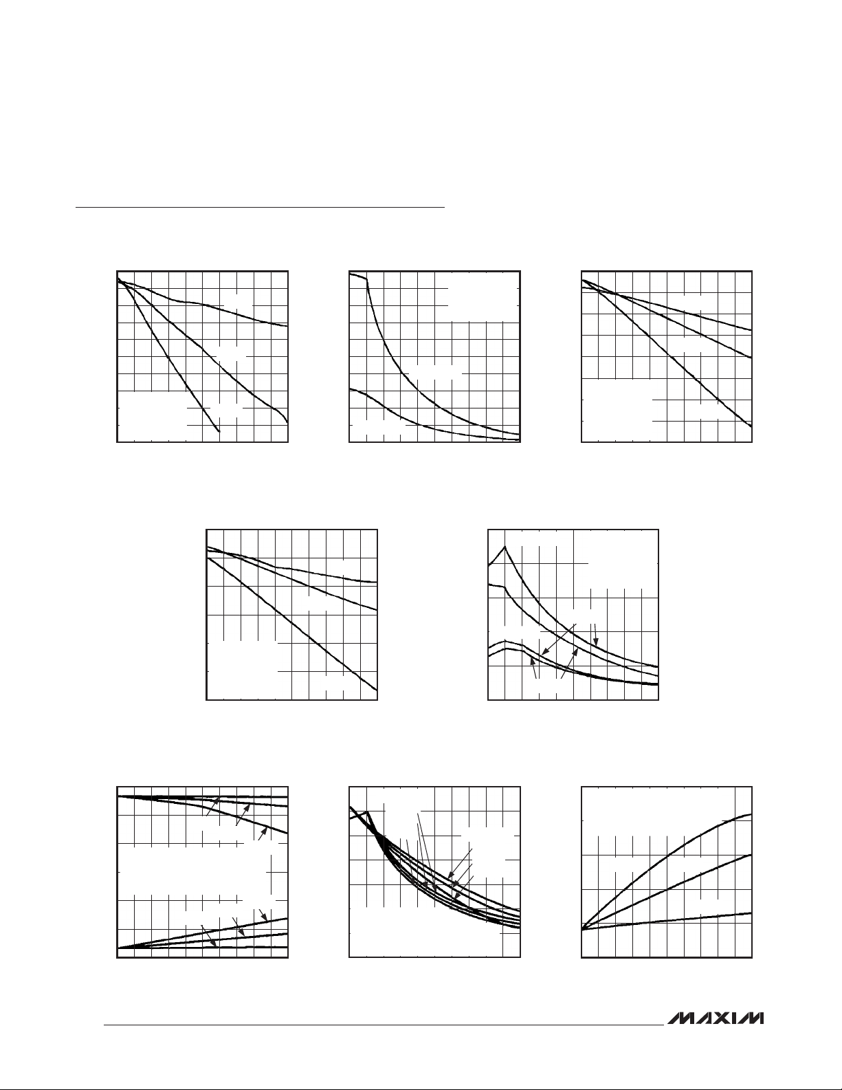
Typical Operating Characteristics
MAX200/204/205/206/207/208/211/213
TRANSMITTER OUTPUT VOLTAGE
vs. LOAD CAPACITANCE
7.0
6.8
6.6
6.4
6.2
6.0
5.8
5.6
Tx OUTPUT VOLTAGE (IVI)
VCC = +5V
5.4
ALL Tx OUTPUTS
LOADED 3kIIIC
5.2
TA = +25NC
5.0
0 5000
L
LOAD CAPACITANCE (pF)
20kbps
MAX200-MAX213 toc01
60kbps
116kbps
400030001000 2000
MAX201
TRANSMITTER OUTPUT VOLTAGE
vs. LOAD CAPACITANCE
10.0
9.5
9.0
8.5
8.0
VCC = +5V
Tx OUTPUT VOLTAGE (IVI)
ALL Tx OUTPUTS
LOADED 3kIIIC
7.5
MAX200–MAX209/MAX211/MAX213
7.0
TA = +25NC
V+ = 12V
L
LOAD CAPACITANCE (pF)
MAX202/203
TRANSMITTER OUTPUT VOLTAGE
vs. LOAD CAPACITANCE
7.5
5.0
2.5
VCC = +4.5V, TA = +25NC
BOTH Tx OUTPUTS, LOADED 3kΩIIC
0
ONE TRANSMITTER AT FULL DATA RATE
ONE TRANSMITTER AT 1/8 DATA RATE
-2.5
Tx OUTPUT VOLTAGE (V)
-5.0
-7.0
20kbps
120kbps
120kbps
20kbps
LOAD CAPACITANCE (pF)
240kbps
MAX200-MAX213 toc06
L
240kbps
400030001000 20000 5000
MAX200/204/205/206/207/208/211/213
TRANSMITTER SKEW RATE
vs. LOAD CAPACITANCE
22
20
18
16
14
12
10
Tx SLEW RATE (V/Fs)
8
6
4
+SLEW RATE
2
0 5000
20kbps
60kbps
112kbps
400030001000 20000 5000
-SLEW RATE
LOAD CAPACITANCE (pF)
MAX200-MAX213 toc04
MAX202/203
TRANSMITTER SLEW RATE
vs. LOAD CAPACITANCE
14
12
10
8
6
Tx SLEW RATE (V/Fs)
4
2
0
+SLEW RATE
20kbps
120kbps
240kbps
VCC = +4.5V, TA = +25NC
BOTH Tx OUTPUTS, LOADED 3kΩIIC
ONE TRANSMITTER AT FULL DATA RATE
ONE TRANSMITTER AT 1/8 DATA RATE
LOAD CAPACITANCE (pF)
VCC = +5V
ALL Tx OUTPUTS
LOADED 3kIIIC
TA = +25NC
400030001000 2000
25
20
15
10
+SLEW RATE
Tx SLEW RATE (V/Fs)
5
0
-SLEW RATE
20kbps
120kbps
240kbps
L
400030001000 20000 5000
L
MAX200-MAX213 toc02
MAX201/MAX209
TRANSMITTER SLEW RATE
vs. LOAD CAPACITANCE
-SLEW RATE
MAX201
LOAD CAPACITANCE (pF)
MAX200-MAX213 toc07
TRANSMITTER OUTPUT VOLTAGE
vs. LOAD CAPACITANCE
10.0
9.8
9.6
9.4
9.2
9.0
VCC = +5V
Tx OUTPUT VOLTAGE (IVI)
ALL Tx OUTPUTS
8.8
LOADED 3kIIIC
8.6
TA = +25NC
V+ = 12V
8.4
LOAD CAPACITANCE (pF)
VCC = +5V
ALL Tx OUTPUTS
LOADED 3kIIIC
TA = +25NC
V+ = 12V
MAX209
400030001000 20000 5000
MAX202/203
SUPPLY CURRENT
vs. LOAD CAPACITANCE
35
VCC = +4.5V, TA = +25NC,
BOTH Tx OUTPUTS, LOADED 3kΩIIC
ONE TRANSMITTER AT FULL DATA RATE
30
ONE TRANSMITTER AT 1/8 DATA RATE
25
20
SUPPLY CURRENT (mA)
15
10
240kbps
LOAD CAPACITANCE (pF)
MAX209
L
L
MAX200-MAX213 toc05
20kbps
MAX200-MAX213 toc03
60kbps
116kbps
400030001000 20000 5000
L
MAX200-MAX213 toc08
120kbps
20kbps
400030001000 20000 5000
4
Page 5
I
SHDN
+5.5V
0.1FF
0V OR +5.5V
DRIVE
0.1FF
0.1FF
+5.5V
+5.5V (0)
C1+
C1-
C2+
C2-
400kI
T
IN
R
OUT
EN (EN)
SHDN
(SHDN)
NOTE 1: ( ) ARE FOR MAX213.
NOTE 2: CAPACITORS CAN BE POLARIZED OR UNPOLARIZED.
+5.5V
V
MAX200
MAX205
MAX206
MAX211
MAX213
R1 T0 R5
GND
CC
T1 T0 T5
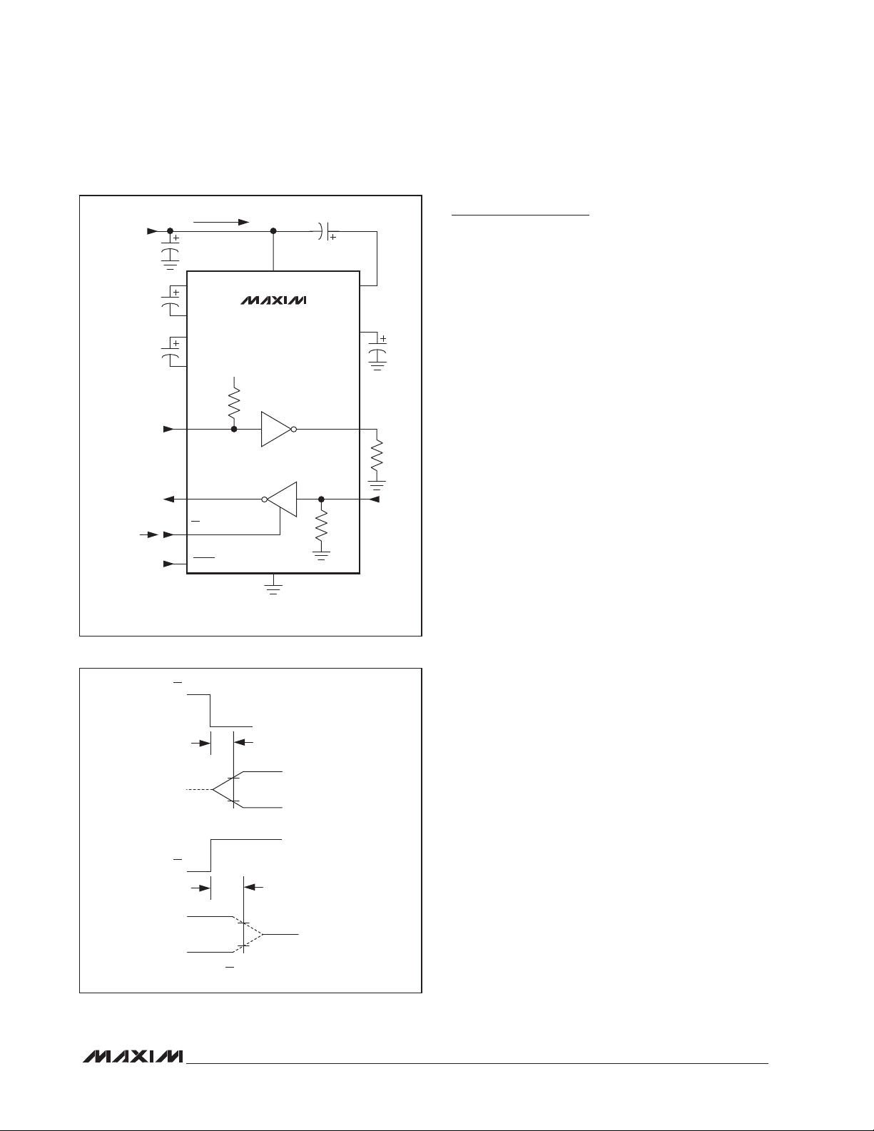
Figure 1. Shutdown Current Test Circuit
EN
INPUT
+3V
0V
OUTPUT ENABLE TIME
+3.5V
RECEIVER
OUTPUT
C
= 150pF
L
0V
EN
INPUT
V
RECEIVER
OUTPUTS
NOTE: POLARITY OF EN IS REVERSED FOR THE MAX213.
OH
V
+0.8V
+3V
OUTPUT ENABLE TIME
VOH - 0.1V
OL
V
OL
RL = 1kI
+ 0.1V
+5V, RS-232 Transceivers
with 0.1µF External Capacitors
Detailed Description
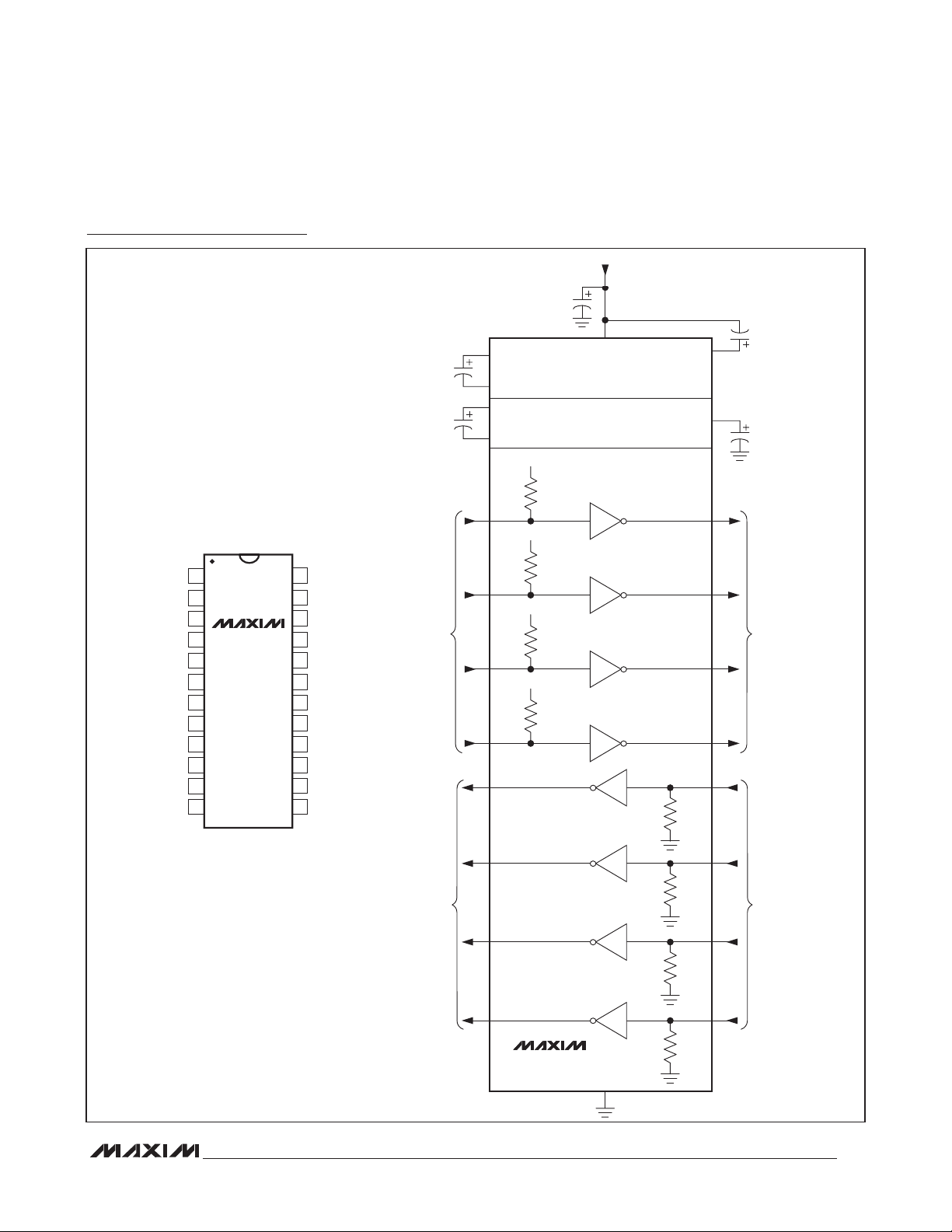
The MAX200–MAX209/MAX211/MAX213 consist of
three sections: charge-pump voltage converters, drivers
(transmitters), and receivers. Each section is described
in detail.
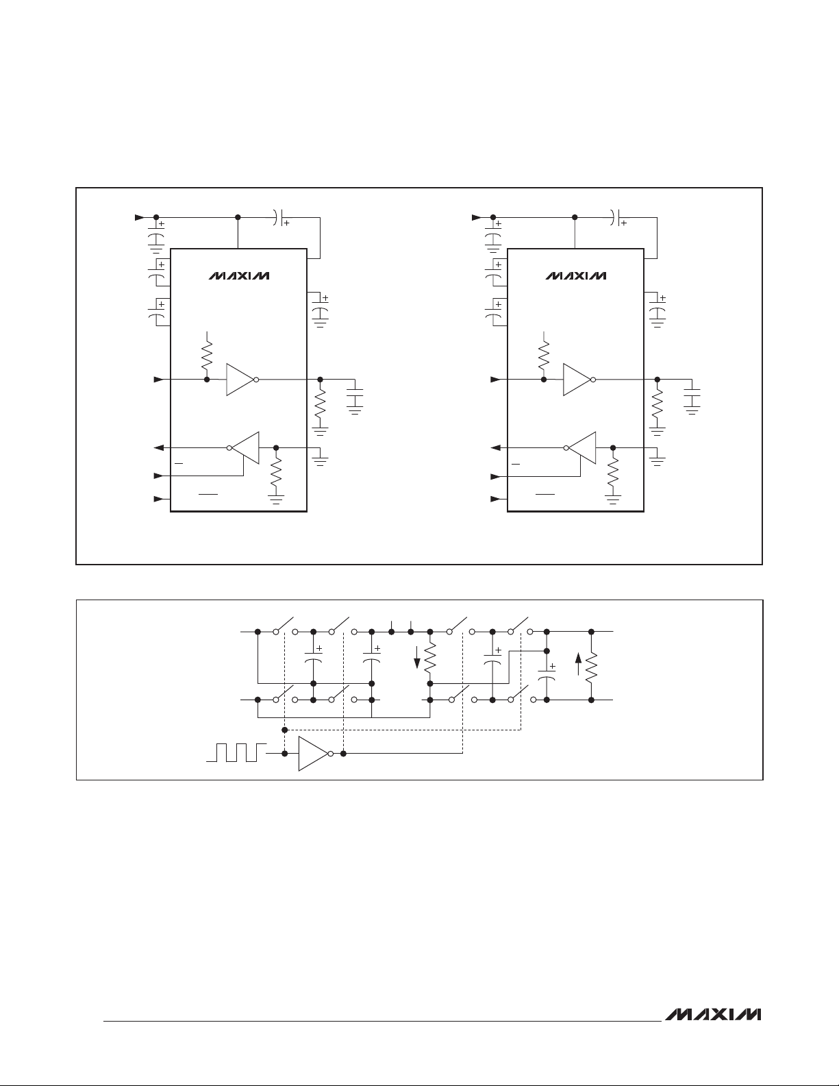
+5V to ±10V Dual Charge-Pump
Voltage Converter
The +5V to Q10V conversion is performed by two
charge-pump voltage converters (Figure 4). The first
uses capacitor C1 to double +5V to +10V, storing +10V
on the V+ output filter capacitor, C3. The second chargepump voltage converter uses capacitor C2 to invert +10V
to -10V, storing -10V on the V- output filter capacitor, C4.
The MAX201 and MAX209 include only the V+ to Vcharge pump, and are intended for applications that
have a VCC = +5V supply and a V+ supply in the +9V to
+13.2V range.
In shutdown mode, V+ is internally connected to VCC by
a 1kI pulldown resistor and V- is internally connected to
ground by a 1kI pullup resistor.
RS-232 Drivers
When VCC = +5V, the typical driver output-voltage swing
is Q8V when loaded with a nominal 5kI RS-232 receiver.
The output swing is guaranteed to meet the EIA/TIA-232E
and V.28 specifications, which call for Q5V minimum out-
put levels under worst-case conditions. These include
a minimum 3kI load, VCC = +4.5V, and the maximum
operating temperature. The open-circuit output-voltage
swing ranges from (V+ - 0.6V) to V-.
Input thresholds are both CMOS and TTL compatible.
The inputs of unused drivers can be left unconnected
since 400kI pullup resistors to VCC are included onchip. Since all drivers invert, the pullup resistors force
the outputs of unused drivers low. The input pullup resistors typically source 15µA; therefore, the driver inputs
should be driven high or open circuited to minimize
power-supply current in shutdown mode.
When in low-power shutdown mode, the driver outputs
are turned off and their leakage current is less than 1mA,
even if the transmitter output is backdriven between 0V
and (VCC + 6V). Below -0.5V, the transmitter output is
diode clamped to ground with a 1kI series impedance.
The transmitter output is also zener clamped to approximately (VCC + 6V), with a 1kI series impedance.
+ 2.5V
0.1FF
5kI
V+
V-
0.1FF
T
OUT
3kI
R
IN
+5.5V
MAX200–MAX209/MAX211/MAX213
Figure 2. Receiver Output Enable and Disable Timing
5
Page 6
+5V, RS-232 Transceivers
with 0.1µF External Capacitors
0.1FF
+5V
0.1FF
V
CC
MAX200-MAX209
MAX211
MAX213
+5V
T1 T0 T5
R1 T0 R5
MINIMUM SLEW-RATE
TEST CIRCUIT
0.1FF
0.1FF
0V (+5V)
0V (+5V)
C1+
C1C2+
C2-
400kI
T
IN
R
OUT
EN (EN)
SHDN (SHDN)
NOTE: ( ) ARE FOR MAX213.
Figure 3. Transition Slew-Rate Test Circuit
T
5kI
OUT
+5V
0.1FF
V+
0.1FF
V-
0.1FF 0.1FF
2500pF
3kI
R
IN
0.1FF
0V (+5V)
0V (+5V)
C1+
C1C2+
C2-
400kI
T
IN
R
OUT
EN (EN)
SHDN (SHDN)
V
CC
MAX200-MAX209
MAX211
MAX213
+5V
T1 T0 T5
R1 T0 R5
MAXIMUM SLEW-RATE
TEST CIRCUIT
0.1FF
T
5kI
OUT
V+
V-
50pF
7kI
R
IN
V+ V+
V
CC
C1
MAX200–MAX209/MAX211/MAX213
GND
S3 S4
200kHz
C3
C1-
I
GND
V
CC
+
L
S5S1 S2C1+ S6C2+
+
R
L
C2
S7
C2-
C4
S8
Figure 4. Dual Charge-Pump Diagram
RS-232 Receivers
The receivers convert RS-232 signals to CMOS logic
output levels. Receiver outputs are inverting, maintaining compatibility with driver outputs. The guaranteed
receiver input thresholds of +0.8V and +2.4V are significantly tighter than the Q3.0V threshold required by the
EIA/TIA-232E specification. This allows receiver inputs
to respond to TTL/CMOS logic levels and improves noise
margin for RS-232 levels.
The MAX200–MAX209/MAX211/MAX213 guaranteed
+0.8V threshold (+0.6V in shutdown for the MAX213)
ensures that receivers shorted to ground have a logic 1
output. Also, the 5kI input resistance to ground ensures
that a receiver with its input left open also has a logic 1
output.
Receiver inputs have approximately +0.5V hysteresis.
This provides clean output transitions, even with slow
rise and fall time input signals with moderate amounts of
noise and ringing. In shutdown, the MAX213 receivers
R4 and R5 have no hysteresis.
GND
IL-
-
R
L
V-
6
Page 7
+5V, RS-232 Transceivers
with 0.1µF External Capacitors
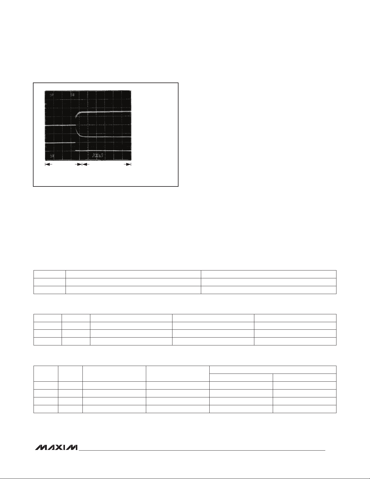
TWO TRANSMITTER
OUTPUTS:
ONE HIGH, ONE LOW
SHDN*
SHUTDOWN TRANSMITTERS ON
THREE TRANSMITTERS LOADED WITH 3kI||2500pF.
*SHUTDOWN POLARITY REVERSED FOR MAX213.
Figure 5. Transmitter Outputs When Exiting Shutdown
Shutdown and Enable Control
In shutdown mode, the MAX200/MAX205/MAX206/
MAX211/MAX213 charge pumps are turned off, V+ is
pulled down to VCC, V- is pulled to ground, and the
transmitter outputs are disabled. This reduces supply
current typically to 1µA (15µA for the MAX213). The time
MAX200–MAX209/MAX211/MAX213
required to exit shutdown is 1ms, as shown in Figure 5.
All receivers except R4 and R5 on the MAX213 are put
into a high-impedance state in shutdown mode. The
MAX213’s R4 and R5 receivers still function in shutdown
mode. These two receivers are useful for monitoring
external activity while maintaining minimal power consumption.
The enable control is used to put the receiver outputs
into a high-impedance state, so that the receivers can be
connected directly to a three-state bus. It has no effect
on the RS-232 drivers or on the charge pumps.
MAX213 Receiver Operation in Shutdown
During normal operation, the MAX213’s receiver propagation delay is typically 1Fs. When entering shutdown
with receivers active, R4 and R5 are not valid until 80Fs
after SHDN is driven low. In shutdown mode, propagation delays increase to 4Fs for a high-to-low or a low-tohigh transition.
When exiting shutdown, all receiver outputs are invalid
until the charge pumps reach nominal values (< 2ms
when using 0.1FF capacitors).
Table 1a. MAX200 Control Pin Configurations
SHDN OPERATION STATUS TRANSMITTERS T1–T5
0 Normal Operation All Active
1 Shutdown All High-Z
Table 1b. MAX205/MAX206/MAX211 Control Pin Configurations
SHDN
0 0 Normal Operation All Active All Active
0 1 Normal Operation All Active All High-Z
1 0 Shutdown All High-Z All High-Z
EN
OPERATION STATUS TRANSMITTERS T1–T5 RECEIVERS R1–R5
Table 1c. MAX213 Control Pin Configurations
SHDN
0 0 Shutdown All High-Z High-Z High-Z
0 1 Shutdown All High-Z High-Z Active*
1 0 Normal Operation All Active High-Z High-Z
1 1 Normal Operation All Active Active Active
*Active = active with reduced performance.
EN OPERATION STATUS TRANSMITTERS T1–T4
R1, R2, R3 R4, R5
RECEIVERS
7
Page 8

+5V, RS-232 Transceivers
with 0.1µF External Capacitors
Applications Information
Capacitor Selection
The type of capacitor used is not critical for proper
operation. Ceramic capacitors are suggested. To ensure
proper RS-232 signal levels over temperature when
using 0.1FF capacitors, make sure the capacitance
value does not degrade excessively as the temperature
varies. If in doubt, use capacitors with a larger nominal
value. Also observe the capacitors’ ESR value over temperature, since it influences the amount of ripple on V+
and V-. To reduce the output impedance at V+ and V-,
use larger capacitors (up to 10FF). If polarized capacitors are used, obey the polarities shown in Figure 1 and
the pin configurations.
Driving Multiple Receivers
Each transmitter is designed to drive a single receiver.
Transmitters can be paralleled to drive multiple receivers.
Driver Outputs When Exiting Shutdown
Figure 5 shows two driver outputs exiting shutdown. As
they become active, the two driver outputs go to opposite RS-232 levels (one driver input is high, the other
is low). Each driver is loaded with 3kI in parallel with
2500pF. The driver outputs display no ringing or undesirable transients as they come out of shutdown.
Power-Supply Decoupling
In applications that are sensitive to power-supply noise,
decouple VCC to ground with a capacitor of the same
value as the charge-pump capacitors.
V+ and V- as Power Supplies
A small amount of power can be drawn from V+ and V-,
although this reduces noise margins.
Power Supplies for MAX201/MAX209
If at power-up the V+ supply rises after the VCC supply,
place a diode (e.g., 1N914) in series with the V+ supply.
Table 2. Summary of EIA/TIA-232E, V.28 Specifications
PARAMETER CONDITION EIA/TIA-232E, V.28 SPECIFICATION
Driver Output Voltage: 0 Level
Driver Output Voltage: 1 Level
Output Level, Maximum No load
Data Rate
Receiver Input Voltage: 0 Level — +3.0V to +15V
Receiver Input Voltage: 1 Level — -3.0V to -15V
Input Level, Maximum —
Instantaneous Slew Rate, Maximum
MAX200–MAX209/MAX211/MAX213
Driver Output Short-Circuit Current, Maximum — 100mA
Transition Rate on Driver Output
Driver Output Resistance -2V < V
3kI to 7kI load
3kI to 7kI load
3kI P RL P 7kI, CL P 2500pF
3kI P RL P 7kI, CL P 2500pF 30V/Fs
V.28 1ms or 3% of the period
EIA/TIA-232E 4% of the period
< +2V
OUT
+5.0V to +15V
-5.0V to -15V
Up to 20kbps
Q25V
Q25V
300I
Table 3. DB9 Cable Connections Commonly Used for EIA/TIA-232E and V.24
Asynchronous Interfaces
PIN NAME CONNECTION
1 Received Line Signal Detector, sometimes called Carrier Detect (DCD) Handshake from DCE
2 Receive Data (RD) Data from DCE
3 Transmit Data (TD) Data from DTE
4 Data Terminal Ready Handshake from DTE
5 Signal Ground Reference point for signals
6 Data Set Ready (DSR) Handshake from DCE
7 Request to Send (RTS) Handshake from DTE
8 Clear to Send (CTS) Handshake from DCE
9 Ring Indicator Handshake from DCE
8
Page 9

+5V, RS-232 Transceivers
with 0.1µF External Capacitors
MAX200 Pin Configuration/Typical Operating Circuit
+5V INPUT
0.1FF
0.1FF
+6.3V
0.1FF
+16V
8
C1+
10
C1-
11
C2+
12
C2-
VOLTAGE DOUBLER
VOLTAGE INVERTER
+5V
7
V
CC
+5V TO +10V
+10V TO -10V
V+
V-
0.1FF
+6.3V
9
13
0.1FF
+16V
MAX200–MAX209/MAX211/MAX213
TOP VIEW
T3
OUT
T1
OUT
T2
OUT
IN
T1
IN
GND
V
CC
400kI
T1
IN
5 2
1
2
3
4
MAX200
5
6
7
T4
20
OUT
19
T5
IN
N.C.
18
SHNDT2
17
16
T5
OUT
15
T4
IN
14
T3
IN
138 V-C1+
129 C2-V+
1110 C2+C1-
TTL/CMOS
INPUTS
15
+5V
T2
IN4 3
+5V
T3
IN14
+5V
T4
IN
+5V
T1
400kI
T2
400kI
T3
400kI
T4
T1
OUT
T2
OUT
T3
1
OUT
T4
OUT
RS-232
OUTPUTS
20
DIP/SO
400kI
T5
IN19 16
18
N.C. SHDN
T5
MAX200
GND
6
T5
OUT
17
9
Page 10

+5V, RS-232 Transceivers
with 0.1µF External Capacitors
MAX201 Pin Configurations/Typical Operating Circuit
+5V INPUT +9V TO +12V
0.1FF
TOP VIEW
C+
C-
V-
T2
OUT
R2
IN
R2
OUT
T2
IN
1
(10) 8
C+
2
C-
T1
IN
T2
7
IN
VOLTAGE CONVERTER
+5V
400kI
+5V
400kI
1
2
3
4
MAX201
5
6
7
V+
14
V
13
CC
GND
12
T1
OUT
11
R1
IN
10
R1
OUT
9
T1
IN
8
0.1FF
+16V
TTL/CMOS
INPUTS
DIP
13 (15)
V
CC
+12V TO -12V
T1
T2
14 (16)
V+
3
V-
T1
OUT
T2
OUT
C2
0.1FF
+16V
11 (13)
RS-232
OUTPUTS
4
C+
1
C-
2
V-
3
T2
4
OUT
R2
IN
R2
OUT
T2
IN
MAX200–MAX209/MAX211/MAX213
MAX201
5
6
7
8
V+
16
V
CC
15
GND
14
T1
13
OUT
R1
12
IN
R1
11
OUT
10
T1
IN
9
N.C.N.C.
TTL/CMOS
OUTPUTS
(11) 9
R1
OUT
6
R2
OUT
MAX201
SO
NOTE: PIN NUMBERS IN ( ) ARE FOR SO PACKAGE
GND
R1
R2
12 (14)
5kI
5kI
R1
IN 10 (12)
R2
IN
RS-232
INPUTS
5
10
Page 11

+5V, RS-232 Transceivers
with 0.1µF External Capacitors
MAX202 Pin Configuration/Typical Operating Circuit
MAX200–MAX209/MAX211/MAX213
TOP VIEW
C1+
1
V+
2
C1-
3
C2+
4
5
C2-
6
V-
T2
7
OUT
R2
8
IN
DIP/SO/WIDE SO
MAX202
+5V INPUT
0.1FF
16
1
0.1FF
+6.3V
0.1FF
+16V
V
16
CC
GND
15
T1
OUT
14
R1
13
IN
R1
12
OUT
11
T1
IN
10
T2
IN
R2
9
OUT
TTL/CMOS
INPUTS
TTL/CMOS
OUTPUTS
C1+
3
C1-
4
C2+
5
C2-
+5V
T1
IN
11
+5V
T2
10
IN
R1
OUT12
R2
OUT
9
V
CC
+5V TO +10V
VOLTAGE DOUBLER
+10V TO -10V
VOLTAGE INVERTER
400kI
T1
400kI
T2
R1
R2
0.1FF
+6.3V
5kI
5kI
2
+10V
V+
-10V
6
V-
T1
OUT
T2
OUT
R1
IN 13
R2
IN
0.1FF
+16V
14
RS-232
OUTPUTS
7
RS-232
INPUTS
8
MAX202
GND
15
11
Page 12

+5V, RS-232 Transceivers
with 0.1µF External Capacitors
MAX203 Pin Configurations/Typical Operating Circuit
+5V INPUT
TOP VIEW
0.1FF
1
T2
IN
2
T1
IN
3
R1
OUT
4
IN
T1
OUT
GND
CC
MAX203
5
6
7
R2
20
OUT
19
R2
IN
T2
18
OUT
17
V-R1
16
C2-
15
C2+
14
V+V
138 C1-C1+
129 V-GND
1110 C2+C2-
TTL/CMOS
INPUTS
+5V
T1
2
T2
1
R1
3
400kI
IN
+5V
400kI
IN
OUT
7
V
CC
T1
OUT
T1
T2
R1
5
RS-232
OUTPUTS
T2
OUT
18
R1
IN 4
DIP
1
T2
IN
2
T1
IN
3
R1
OUT
4
IN
T1
OUT
GND
MAX200–MAX209/MAX211/MAX213
CC
MAX203
5
6
7
R2
20
OUT
19
R2
IN
18
T2
OUT
17
V-R1
16
C2-
15
C2+
14
C1-V
138 C1+V+
129 C2+GND
1110 C2-V-
SO
TTL/CMOS
OUTPUTS
DO NOT MAKE
CONNECTION TO
THESE PINS
INTERNAL -10V
POWER SUPPLY
INTERNAL +10V
POWER SUPPLY
R2
OUT
20
8 (13)
C1+ C2+
13 (14)
C1-
12 (10)
V-
17
V-
14 (8)
V+
NOTE: PIN NUMBERS IN ( ) ARE FOR SO PACKAGE.
GND GND
6 9
R2
MAX203
5kI
5kI
R2
C2+
C2-
C2-
IN
RS-232
INPUTS
19
11 (12)
15
16
10 (11)
12
Page 13

+5V, RS-232 Transceivers
with 0.1µF External Capacitors
MAX204 Pin Configuration/Typical Operating Circuit
+5V INPUT
0.1FF
TOP VIEW
0.1FF
+6.3V
0.1FF
+16V
7
C1+
9
C1-
10
C2+
11
C2-
+5V
6
V
CC
+5V TO +10V
VOLTAGE DOUBLER
+10V TO -10V
VOLTAGE INVERTER
V+
V-
0.1FF
+6.3V
8
12
0.1FF
+16V
MAX200–MAX209/MAX211/MAX213
T1
T2
OUT
OUT
T2
T1
GND
V
C1+
T3
OUT
1
2
3
IN
4
IN
CC
V+
MAX204
5
6
7
8
16
T4
OUT
15
T4
IN
14
T3
IN
13
V-
12
C2-
11
C2+
10
C1-
9
TTL/CMOS
INPUTS
T1
4
T2
3
T3
13
DIP/SO
T4
14
400kI
T1
IN
+5V
IN
+5V
IN
+5V
IN
T1
400kI
T2
400kI
T3
400kI
T4
OUT
1
T2
OUT
2
RS-232
OUTPUTS
T3
OUT
16
T4
OUT
15
MAX204
GND
5
13
Page 14

+5V, RS-232 Transceivers
with 0.1µF External Capacitors
MAX205 Pin Configuration/Typical Operating Circuit
+5V INPUT
0.1FF
12
V
400kI
400kI
400kI
400kI
400kI
CC
T1
3
5kI
5kI
5kI
OUT
T2
4
OUT
T3
2
OUT
T4
OUT
T5
OUT
R1
IN
R2
IN
R3
IN
RS-232
OUTPUTS
1
19
10
5
24
RS-232
INPUTS
T1
T2
T3
T4
T5
R1
R2
R3
+5V
T1
IN
8
+5V
T2
IN
7
+5V
T3
IN
TTL/CMOS
INPUTS
15
+5V
TOP VIEW
T4
IN
1
T4
OUT
2
T3
OUT
T1
3
OUT
T2
4
OUT
R2
IN
R2
OUT
T2
IN
T1
IN
R1
MAX200–MAX209/MAX211/MAX213
OUT
R1
IN
GND
V
CC
MAX205
5
6
7
8
9
11
DIP
24
23
22
21
20
19
18
17
16
1510T3
14
1312R5
R3
IN
R3
OUT
T5
IN
SHDN
EN
T5
OUT
R4
IN
R4
OUT
T4
IN
IN
R5
OUT
IN
TTL/CMOS
OUTPUTS
16
+5V
T5
IN
22
R1
9
OUT
R2
6
OUT
R3
23
OUT
14
5kI
5kI
R4
R5
SHDN
18
IN
13
IN
21
R4
17
OUT
R5
14
OUT
EN
20
R4
R5
MAX205
GND
11
Page 15

+5V, RS-232 Transceivers
with 0.1µF External Capacitors
MAX206 Pin Configuration/Typical Operating Circuit
+5V INPUT
0.1FF
TOP VIEW
T3
OUT
T1
OUT
T2
OUT
IN
R1
OUT
T2
IN
T1
IN
GND
V
CC
9
V
10
0.1FF
+6.3V
0.1FF
+16V
1
2
3
MAX206
4
5
6
7
24
23
22
21
20
19
18
178 R3
169 R3
1510 V-C1+
1411 C2-V+
1312 C2+C1-
T4
OUT
R2
IN
R2
OUT
SHDNR1
EN
T4
IN
T3
IN
OUT
IN
TTL/CMOS
INPUTS
C1+
12
C1-
13
C2+
14
C2-
+5V
400kI
T1
IN
7
+5V
400kI
T2
6
IN
+5V
400kI
T3
IN
18
+5V
400kI
T4
IN
19
CC
+5V TO +10V
VOLTAGE DOUBLER
+10V TO -10V
VOLTAGE INVERTER
T1
T2
T3
T4
V+
V-
T1
OUT
T2
OUT
T3
OUT
T4
OUT
0.1FF
+6.3V
11
15
0.1FF
+16V
2
3
RS-232
OUTPUTS
1
24
MAX200–MAX209/MAX211/MAX213
DIP/SO
TTL/CMOS
OUTPUTS
5kI
5kI
5kI
R1IN4
R2
R3
SHDN
IN
23
RS-232
INPUTS
IN
16
21
R1
OUT
5
R2
OUT
22
R3
OUT
17
EN
20
R1
R2
R3
MAX206
GND
8
15
Page 16
+5V, RS-232 Transceivers
with 0.1µF External Capacitors
MAX207 Pin Configuration/Typical Operating Circuit
+5V INPUT
0.1FF
0.1FF
+6.3V
11
15
0.1FF
+16V
2
TOP VIEW
0.1FF
+6.3V
0.1FF
+16V
10
C1+
12
C1-
13
C2+
14
C2-
+5V
400kI
T1
IN
7
+5V
9
V
CC
+5V TO +10V
VOLTAGE DOUBLER
+10V TO -10V
VOLTAGE INVERTER
T1
V+
V-
T1
OUT
T3
1
OUT
T1
2
OUT
T2
3
OUT
R1
4
IN
R1
OUT
T2
IN
T1
IN
GND
V
CC
MAX207
5
6
7
MAX200–MAX209/MAX211/MAX213
24
23
22
21
20
19
18
178 R3
169 R3
1510 V-C1+
1411 C2-V+
1312 C2+C1-
T4
OUT
R2
IN
R2
OUT
T5
IN
T5
OUT
T4
IN
T3
IN
OUT
IN
TTL/CMOS
INPUTS
T2
6
T3
18
T4
19
T5
21
400kI
IN
+5V
400kI
IN
+5V
400kI
IN
+5V
400kI
IN
T2
T3
T4
T5
DIP/SO/SSOP
R1
5
TTL/CMOS
OUTPUTS
OUT
R2
22
OUT
R3
17
OUT
R1
R2
R3
5kI
5kI
T2
OUT
3
T3
OUT
T4
OUT
T5
OUT
R1
IN
R2
IN 23
R3
IN
RS-232
1
OUTPUTS
24
20
4
RS-232
INPUTS
16
16
MAX207
5kI
GND
8
Page 17
+5V, RS-232 Transceivers
with 0.1µF External Capacitors
MAX208 Pin Configuration/Typical Operating Circuit
+5V INPUT
0.1FF
0.1FF
+6.3V
11
15
0.1FF
+16V
2
TOP VIEW
0.1FF
+6.3V
0.1FF
+16V
9
V
10
C1+
12
C1-
13
C2+
14
C2-
+5V
400kI
T1
IN
5
+5V
CC
+5V TO +10V
VOLTAGE DOUBLER
+10V TO -10V
VOLTAGE INVERTER
T1
V+
V-
T1
OUT
MAX200–MAX209/MAX211/MAX213
T2
1
OUT
T1
2
OUT
R2
3
IN
R2
OUT
T1
IN
R1
OUT
R1
IN
GND
V
CC
MAX208
4
5
6
7
24
23
22
21
20
19
18
178 R4
169 R4
1510 V-C1+
1411 C2-V+
1312 C2+C1-
T3
OUT
R3
IN
R3
OUT
T4
IN
T4
OUT
T3
IN
T2
IN
OUT
IN
TTL/CMOS
INPUTS
T2
18
T3
19
T4
21
R1
6
IN
IN
IN
OUT
+5V
+5V
400kI
400kI
400kI
T2
OUT
5kI
1
RS-232
OUTPUTS
T3
OUT
24
T4
OUT
20
R1
IN
7
T2
T3
T4
R1
DIP/SO
TTL/CMOS
OUTPUTS
R2
OUT
4
R3
22
OUT
R4
OUT
17
R2
R3
R4
5kI
5kI
R2
R3
R4
IN
IN
IN 16
3
RS-232
INPUTS
23
MAX208
5kI
GND
8
17
Page 18

+5V, RS-232 Transceivers
with 0.1µF External Capacitors
MAX209 Pin Configuration/Typical Operating Circuit
+5V INPUT
9V - 13.2V
INPUT
0.1FF
4 5
V+
R1
5kI
8
0.1FF
+16V
T1
OUT
19
T2
OUT
T3
OUT
R1
IN
RS-232
20
OUTPUTS
13
2
TOP VIEW
R1
OUT
R1
IN
GND
V
CC
V+
C+
C-
V-
R5
IN
OUT
OUT
R4
IN
6
0.1FF
+16V
1
2
3
MAX209
4
5
6
7
24
23
22
21
20
19
18
178 R3
169 T3
1510 N.C.R5
1411 ENR4
1312 T3
T1
IN
T2
IN
R2
OUT
R2
IN
T2
OUT
T1
OUT
R3
IN
OUT
IN
OUT
TTL/CMOS
INPUTS
C+
7
C-
+5V
400kI
T1
IN
24
+5V
400kI
T2
23
IN
+5V
400kI
T3
IN
16
R1
OUT
1
V
CC
+10V TO +10V
VOLTAGE INVERTER
T1
T2
T3
DIP/SO
R2
22
OUT
R2
MAX200–MAX209/MAX211/MAX213
R3
OUT
17
R4
OUT
11
R5
10
OUT
EN
14
R3
R4
R5
MAX209
GND
3
18
TTL/CMOS
OUTPUTS
5kI
5kI
5kI
5kI
R2
R3
R4
R5
N.C.
IN
21
IN
18
RS-232
INPUTS
IN
12
IN
9
15
Page 19

+5V, RS-232 Transceivers
with 0.1µF External Capacitors
MAX211 Pin Configuration/Typical Operating Circuit
+5V INPUT
0.1FF
TOP VIEW
T3
OUT
T1
OUT
T2
OUT
R2
IN
R2
OUT
T2
IN
T1
IN
R1
OUT
R1
IN
GND
V
CC
C1+
V+
C1-
1
2
3
4
5
6
7
8
9
10
11
13
MAX211
SO/SSOP
28
T4
R3
27
R3
26
SHDN
25
24
EN
R4
23
R4
22
T4
21
T3
20
19
R5
18
R5
1712V-
16
C2-
1514C2+
OUT
IN
OUT
IN
OUT
IN
IN
OUT
IN
TTL/CMOS
INPUTS
0.1FF
+6.3V
0.1FF
+16V
11
12
C1+
14
C1-
15
C2+
16
C2-
+5V
T1
7
IN
+5V
T2
6
IN
+5V
20
T3
IN
+5V
T4
21
IN
8
R1
OUT
5
R2
OUT
V
CC
+5V TO +10V
VOLTAGE DOUBLER
+10V TO -10V
VOLTAGE INVERTER
400kI
T1
400kI
T2
400kI
T3
400kI
T4
V+
V-
T1
OUT
T2
OUT
T3
OUT
T4
OUT
R1
R2
R1
5kI
R2
5kI
0.1FF
+6.3V
13
17
0.1FF
+16V
2
3
RS-232
OUTPUTS
1
28
9
IN
4
IN
MAX200–MAX209/MAX211/MAX213
TTL/CMOS
OUTPUTS
26
R3
OUT
R4
22
OUT
R5
19
OUT
EN
24
R3
R4
R5
MAX211
GND
10
5kI
5kI
5kI
R3
R4
R5
SHDN
27
IN
IN
IN
RS-232
INPUTS
23
18
25
19
Page 20

+5V, RS-232 Transceivers
with 0.1µF External Capacitors
MAX213 Pin Configuration/Typical Operating Circuit
+5V INPUT
0.1FF
0.1FF
+6.3V
0.1FF
+16V
11
V
12
C1+
14
C1-
15
C2+
16
C2-
+5V
T1
7
IN
+5V
CC
+5V TO +10V
VOLTAGE DOUBLER
+10V TO -10V
VOLTAGE INVERTER
400kI
T1
V+
V-
T1
OUT
0.1FF
+6.3V
13
17
0.1FF
+16V
2
TOP VIEW
1
T3
OUT
2
T1
OUT
T2
3
OUT
R2
4
IN
R2
5
OUT
T2
IN
T1
IN
R1
OUT
R1
IN
GND
V
MAX200–MAX209/MAX211/MAX213
CC
C1+
V+
MAX213
6
7
8
9
10
11
13
C1-
SO/SSOP
28
T4
R3
27
R3
26
SHDN
25
24
EN
R4IN*
23
R4
22
T4
21
T3
20
19
R5
18
R5
1712V-
16
C2-
1514C2+
OUT
IN
OUT
*
OUT
IN
IN
*
OUT
*
IN
TTL/CMOS
INPUTS
TTL/CMOS
OUTPUTS
6
20
21
8
5
26
22
19
400kI
T2
IN
+5V
T3
IN
+5V
T4
IN
R1
OUT
R2
OUT
R3
OUT
R4
*
OUT
R5
*
OUT
T2
400kI
T3
400kI
T4
R1
R2
R3
R4
R5
5kI
5kI
5kI
5kI
5kI
T2
T3
T4
R1
R2
R3
R4IN*
R5
OUT
OUT
OUT
3
RS-232
OUTPUTS
1
28
9
IN
4
IN
27
IN
*
IN
RS-232
INPUTS
23
18
20
*ACTIVE IN SHUTDOWN
EN
24
MAX213
GND
10
SHDN
25
Page 21

+5V, RS-232 Transceivers
with 0.1µF External Capacitors
Ordering Information
MAX200–MAX209/MAX211/MAX213
PART TEMP RANGE PIN-PACKAGE
MAX200CPP
MAX200CWP
MAX200EPP
MAX200EWP
MAX201CPD
MAX201CWE
MAX201C/D
MAX201EPD
MAX201EWE
MAX202CPE
MAX202CSE
MAX202CWE
MAX202C/D
MAX202EPE
MAX202ESE
MAX202EWE
MAX203CPP
MAX203CWP
MAX203EPP
MAX203EWP
MAX204CPE
MAX204CWE
MAX204C/D
MAX204EPE
MAX204EWE
MAX205CPG
MAX205EPG
MAX206CNG
MAX206CWG
MAX206CAG
MAX206ENG
0NC to +70NC
0NC to +70NC
-40NC to +85NC
-40NC to +85NC
0NC to +70NC
0NC to +70NC
0NC to +70NC
-40NC to +85NC
-40NC to +85NC
0NC to +70NC
0NC to +70NC
0NC to +70NC
0NC to +70NC
-40NC to +85NC
-40NC to +85NC
-40NC to +85NC
0NC to +70NC
0NC to +70NC
-40NC to +85NC
-40NC to +85NC
0NC to +70NC
0NC to +70NC
0NC to +70NC
-40NC to +85NC
-40NC to +85NC
0NC to +70NC
-40NC to +85NC
0NC to +70NC
0NC to +70NC
0NC to +70NC
-40NC to +85NC
20 Plastic DIP
20 Wide SO
20 Plastic DIP
20 Wide SO
14 Plastic DIP
16 Wide SO
Dice*
14 Plastic DIP
16 Wide SO
16 Plastic DIP
16 Narrow SO
16 Wide SO
Dice*
16 Plastic DIP
16 Narrow SO
16 Wide SO
20 Plastic DIP
20 Wide SO
20 Plastic DIP
20 Wide SO
16 Plastic DIP
16 Wide SO
Dice*
16 Plastic DIP
16 Wide SO
24 Wide Plastic DIP
24 Wide Plastic DIP
24 Narrow Plastic DIP
24 Wide SO
24 SSOP
24 Narrow Plastic DIP
PART TEMP RANGE PIN-PACKAGE
MAX206EWG
MAX206EAG
MAX207CNG
MAX207CWG
MAX207CAG
MAX207ENG
MAX207EWG
MAX207EAG
MAX208CNG
MAX208CWG
MAX208CAG
MAX208C/D
MAX208ENG
MAX208EWG
MAX208EAG
MAX209CNG
MAX209CWG
MAX209C/D
MAX209ENG
MAX209EWG
MAX211CWI
MAX211CAI
MAX211C/D
MAX211EWI
MAX211EAI
MAX213CWI
MAX213CAI
MAX213C/D
MAX213EWI
MAX213EAI
*Contact factory for dice specifications.
-40NC to +85NC
-40NC to +85NC
0NC to +70NC
0NC to +70NC
0NC to +70NC
-40NC to +85NC
-40NC to +85NC
-40NC to +85NC
0NC to +70NC
0NC to +70NC
0NC to +70NC
0NC to +70NC
-40NC to +85NC
-40NC to +85NC
-40NC to +85NC
0NC to +70NC
0NC to +70NC
0NC to +70NC
-40NC to +85NC
-40NC to +85NC
0NC to +70NC
0NC to +70NC
0NC to +70NC
-40NC to +85NC
-40NC to +85NC
0NC to +70NC
0NC to +70NC
0NC to +70NC
-40NC to +85NC
-40NC to +85NC
24 Wide SO
24 SSOP
24 Narrow Plastic DIP
24 Wide SO
24 SSOP
24 Narrow Plastic DIP
24 Wide SO
24 SSOP
24 Narrow Plastic DIP
24 Wide SO
24 SSOP
Dice*
24 Narrow Plastic DIP
24 Wide SO
24 SSOP
24 Narrow Plastic DIP
24 Wide SO
Dice*
24 Narrow Plastic DIP
24 Wide SO
28 Wide SO
28 SSOP
Dice*
28 Wide SO
28 SSOP
28 Wide SO
28 SSOP
Dice*
28 Wide SO
28 SSOP
21
Page 22

+5V, RS-232 Transceivers
with 0.1µF External Capacitors
Package Information
For the latest package outline information and land patterns, go to www.maxim-ic.com/packages. Note that a “+”,
“#”, or “-” in the package code indicates RoHS status only. Package drawings may show a different suffix character,
but the drawing pertains to the package regardless of RoHS status.
PACKAGE TYPE
14 CDIP J14-3
16 CDIP J16-3
20 CDIP J20-2
24 CDIP R24-4
14 PDIP P14-3
16 PDIP P16-1
20 PDIP P20-3
24 PDIP N24-2
24 PDIP N24-3
24 PDIP P24-1
24 PDIP P24M-1
16 SO S16-3
16 SO W16-3
16 SO W16-1
20 SO W20M-1
20 SO W20-3
24 SO W24-2
28 SO W28-1
28 SO W28-2
24 SSOP A24-3
24 SSOP A24-2
28 SSOP A28-1
MAX200–MAX209/MAX211/MAX213
16 TSSOP U16-1
PACKAGE CODE DOCUMENT NO.
21-0045
21-0045
21-0045
21-0045
21-0043
21-0043
21-0043
21-0043
21-0043
21-0044
21-0044
21-0041
21-0042
21-0042
21-0042
21-0042
21-0042
21-0042
21-0042
21-0056
21-0056
21-0056
21-0066
22
Page 23

+5V, RS-232 Transceivers
with 0.1µF External Capacitors
Revision History
MAX200–MAX209/MAX211/MAX213
REVISION
NUMBER
6 10/03
7 12/05 Added Note 1 to the Absolute Maximum Ratings section. 2
REVISION
DATE
DESCRIPTION
Changed the Features section and section information to the Next-Generation
Device Features section.
PAGES
CHANGED
1
Maxim cannot assume responsibility for use of any circuitry other than circuitry entirely embodied in a Maxim product. No circuit patent licenses are implied.
Maxim reserves the right to change the circuitry and specifications without notice at any time.
Maxim Integrated Products, 120 San Gabriel Drive, Sunnyvale, CA 94086 408-737-7600 23
©
2005 Maxim Integrated Products Maxim is a registered trademark of Maxim Integrated Products, Inc.
 Loading...