

General Description
The MAX2065 high-linearity, analog/digital variablegain amplifier (VGA) is designed to operate in the
50MHz to 1000MHz frequency range with two independent attenuators (see the
Typical Application Circuit
).
The digital attenuator is controlled as a slave peripheral
using either the SPI™-compatible interface or a parallel
bus with 31dB total adjustment range in 1dB steps. An
added feature allows “rapid-fire” gain selection
between each of four steps, preprogrammed by the
user through the SPI-compatible interface. The 2-pin
control allows the user to quickly access any one of
four customized attenuation states without reprogramming the SPI bus. The analog attenuator is controlled
using an external voltage or through the SPI-compatible
interface using an on-chip 8-bit DAC.
Because each of the three stages has its own RF input
and RF output, this component can be configured to
either optimize NF (amplifier configured first), OIP3 (amplifier last), or a compromise of NF and OIP3. The device’s
performance features include 22dB amplifier gain (amplifier only), 6.5dB NF at maximum gain (includes attenuator
insertion losses), and a high OIP3 level of +42dBm. Each
of these features makes the MAX2065 an ideal VGA for
numerous receiver and transmitter applications.
In addition, the MAX2065 operates from a single +5V
supply with full performance, or a single +3.3V supply
with slightly reduced performance, and has an
adjustable bias to trade current consumption for linearity
performance. This device is available in a compact 40pin thin QFN package (6mm x 6mm) with an exposed
pad. Electrical performance is guaranteed over the
extended temperature range (TC= -40°C to +85°C).
Applications
IF and RF Gain Stages
Temperature Compensation Circuits
Cellular Band WCDMA and cdma2000®Base
Stations
GSM 850/GSM 900 EDGE Base Stations
WiMAX and LTE Base Stations and Customer
Premise Equipment
Fixed Broadband Wireless Access
Wireless Local Loop
Military Systems
Video-on-Demand (VOD) and DOCSIS®-
Compliant EDGE QAM Modulation
Cable Modem Termination Systems (CMTS)
Features
♦ 50MHz to 1000MHz RF Frequency Range
♦ Pin-Compatible Family Includes:
MAX2066 (Digital VGA)
MAX2067 (Analog VGA)
♦ +19.4dB (Typ) Maximum Gain
♦ 0.5dB Gain Flatness Over 100MHz Bandwidth
♦ 62dB Gain Range (31dB Analog + 31dB Digital)
♦ Built-in DAC for Analog Attenuation Control
♦ Supports Four “Rapid-Fire” Preprogrammed
Attenuator States
Quickly Access Any One of Four Customized
Attenuation States Without Reprogramming
the SPI Bus
Ideal for Fast-Attack, High-Level Blocker Protection
Prevents ADC Overdrive Condition
♦ Excellent Linearity (Configured with Amplifier
Last)
+42dBm OIP3
+63dBm OIP2
+19dBm Output 1dB Compression Point
-67dBc HD2
-83dBc HD3
♦ 6.5dB Typical Noise Figure (NF)
♦ Fast, 25ns Digital Switching
♦ Very Low Digital VGA Amplitude Overshoot/
Undershoot
♦ Single +5V Supply (Optional +3.3V Operation)
♦ External Current-Setting Resistors Provide Option
for Operating Device in Reduced-Power/
Reduced-Performance Mode
MAX2065
50MHz to 1000MHz High-Linearity, Serial/
Parallel-Controlled Analog/Digital VGA
________________________________________________________________
Maxim Integrated Products
1
Ordering Information
19-3131; Rev 0; 3/08
For pricing, delivery, and ordering information, please contact Maxim Direct at 1-888-629-4642,
or visit Maxim’s website at www.maxim-ic.com.
+
Denotes a lead-free package.
*
EP = Exposed pad.
T = Tape and reel.
cdma2000 is a registered trademark of Telecommunications
Industry Association.
DOCSIS and CableLabs are registered trademarks of Cable
Television Laboratories, Inc. (CableLabs®).
SPI is a trademark of Motorola, Inc.
Pin Configuration appears at end of data sheet.
PART TEMP RANGE
MAX2065ETL+ -40°C to +85°C 40 Thin QFN-EP* T4066-3
M AX 2065E TL+ T -40°C to +85°C 40 Thin QFN-EP* T4066-3
PINPACKAGE
PKG
CODE
MAX2065
50MHz to 1000MHz High-Linearity, Serial/
Parallel-Controlled Analog/Digital VGA
2 _______________________________________________________________________________________
ABSOLUTE MAXIMUM RATINGS
+3.3V SUPPLY DC ELECTRICAL CHARACTERISTICS
(
Typical Application Circuit
, high-current (HC) mode, VCC= +3.0V to +3.6V, TC= -40°C to +85°C. Typical values are at VCC= +3.3V
and T
C
= +25°C, unless otherwise noted.)
Stresses beyond those listed under “Absolute Maximum Ratings” may cause permanent damage to the device. These are stress ratings only, and functional
operation of the device at these or any other conditions beyond those indicated in the operational sections of the specifications is not implied. Exposure to
absolute maximum rating conditions for extended periods may affect device reliability.
Note 1: Based on junction temperature TJ= TC+ (θJCx VCCx ICC). This formula can be used when the temperature of the exposed
pad is known while the device is soldered down to a printed-circuit board (PCB). See the
Applications Information
section
for details. The junction temperature must not exceed +150°C.
Note 2: Junction temperature T
J
= TA+ (θJAx VCCx ICC). This formula can be used when the ambient temperature of the PCB is
known. The junction temperature must not exceed +150°C.
Note 3: Package thermal resistances were obtained using the method described in JEDEC specification JESD51-7, using a 4-layer
board. For detailed information on package thermal considerations, refer to www.maxim-ic.com/thermal-tutorial
.
Note 4: T
C
is the temperature on the exposed pad of the package. TAis the ambient temperature of the device and PCB.
VCC_ to GND ........................................................-0.3V to +5.5V
VDD_LOGIC, DATA, CS, CLK, SER/PAR, VDAC_EN,
VREF_SELECT.....................................-0.3V to (VCC_ + 0.3V)
STATE_A, STATE_B, D0–D4 ....................-0.3V to (VCC_ + 0.3V)
AMP_IN, AMP_OUT, VREF_IN,
ANALOG_VCTRL ................................-0.3V to (VCC_ + 0.3V)
ATTEN1_IN, ATTEN1_OUT, ATTEN2_IN,
ATTEN2_OUT...................................................-1.2V to + 1.2V
RSET to GND........................................................-0.3V to + 1.2V
RF Input Power (ATTEN1_IN, ATTEN1_OUT,
ATTEN2_IN, ATTEN2_OUT).......................................+20dBm
RF Input Power (AMP_IN)...............................................+18dBm
Continuous Power Dissipation (Note 1) ...............................6.5W
θ
JA
(Notes 2, 3)..............................................................+38°C/W
θ
JC
(Note 3) ...................................................................+10°C/W
Operating Temperature Range (Note 4).....T
C
= -40°C to +85°C
Maximum Junction Temperature .....................................+150°C
Storage Temperature.........................................-65°C to +150°C
Lead Temperature (soldering, 10s) .................................+300°C
+5V SUPPLY DC ELECTRICAL CHARACTERISTICS
(
Typical Application Circuit
, VCC= +4.75V to +5.25V, TC= -40°C to +85°C. Typical values are at VCC= +5V and
T
C
= +25°C, unless otherwise noted.)
PARAMETER SYMBOL CONDITIONS MIN TYP MAX UNITS
Supply Voltage V
Supply Current I
LOGIC INPUTS (DATA, CS, CLK, VDAC_EN, VREF_SELECT, SER/PAR, STATE_A, STATE_B, D0–D4)
Input High Voltage V
Input Low Voltage V
CC
CC
IH
IL
3.0 3.3 3.6 V
Supply Voltage V
Supply Current I
LOGIC INPUTS (DATA, CS, CLK, VDAC_EN, VREF_SELECT, SER/PAR, STATE_A, STATE_B, D0–D4)
Input High Voltage V
Input Low Voltage V
Input Current Logic-High I
Input Current Logic-Low I
PARAMETER SYMBOL CONDITIONS MIN TYP MAX UNITS
CC
CC
IH
IH
IL
Low-current (LC) mode 73 93
High-current (HC) mode 124 146
IL
4.75 5 5.25 V
3V
-1 +1 µA
-1 +1 µA
60 80 mA
2V
0.8 V
mA
0.8 V
MAX2065
50MHz to 1000MHz High-Linearity, Serial/
Parallel-Controlled Analog/Digital VGA
_______________________________________________________________________________________ 3
+5V SUPPLY AC ELECTRICAL CHARACTERISTICS
(
Typical Application Circuit
, VCC= +4.75 to +5.25V, HC mode with each attenuator set for maximum gain, 50MHz ≤ fRF≤ 1000MHz,
T
C
= -40°C to +85°C. Typical values are at VCC= +5.0V, HC mode, PIN= -20dBm, fRF= 200MHz, and TC= +25oC, unless otherwise
noted.) (Note 5)
+3.3V SUPPLY AC ELECTRICAL CHARACTERISTICS
(
Typical Application Circuit
, VCC= +3.0V to +3.6V, TC= -40°C to +85°C. Typical values are at VCC= +3.3V, HC mode with attenua-
tors set for maximum gain, P
IN
= -20dBm, fRF= 200MHz, and TC= +25oC, unless otherwise noted.) (Note 5)
PARAMETER SYMBOL CONDITIONS MIN TYP MAX UNITS
RF Frequency Range f
Small Signal Gain G 18.8 dB
Output Third-Order Intercept
Point
Noise Figure NF Maximum gain setting 6.7 dB
Total Attenuation Range Analog and digital combined 61.5 dB
RF
OIP3 P
(Notes 6, 7) 50 1000 MHz
= 0dBm/tone, maximum gain setting 37.5 dBm
OUT
PARAMETER SYMBOL CONDITIONS MIN TYP MAX UNITS
RF Frequency Range f
Small Signal Gain G
Gain Variation vs. Temperature -0.006 dB/°C
Gain Flatness vs. Frequency
Noise Figure NF
Total Attenuation Range Analog and digital combined 61.5 dB
Output Second-Order Intercept
Point
Output Third-Order Intercept
Point
RF
OIP2 P
OIP3
(Notes 6, 7) 50 1000 MHz
200MHz 19.4
350MHz, TC = +25°C 17.5 18.7 19.7
450MHz 18.2
750MHz 16.4
900MHz 15.6
Any 100MHz frequency band from 50MHz
to 500MHz
200MHz 6.5
350MHz, TC = +25°C (Note 7) 6.8 8
450MHz 7
750MHz 7.8
900MHz 8.2
= 0dBm/tone, Δf = 1MHz, f1 + f
OUT
P
= 0dBm/tone,
OUT
H C m od e, Δ f = 1M H z
P
= 0dBm/tone,
OUT
LC mode, Δf = 1MHz
200MHz 42
350MHz 40
450MHz 39
750MHz 36
900MHz 35
200MHz 40
350MHz 38
450MHz 37
750MHz 35
900MHz 33
2
0.5 dB
63 dBm
dB
dB
dBm
MAX2065
50MHz to 1000MHz High-Linearity, Serial/
Parallel-Controlled Analog/Digital VGA
4 _______________________________________________________________________________________
+5V SUPPLY AC ELECTRICAL CHARACTERISTICS (continued)
(
Typical Application Circuit
, VCC= +4.75 to +5.25V, HC mode with each attenuator set for maximum gain, 50MHz ≤ fRF≤ 1000MHz,
T
C
= -40°C to +85°C. Typical values are at VCC= +5.0V, HC mode, PIN= -20dBm, fRF= 200MHz, and TC= +25oC, unless otherwise
noted.) (Note 5)
PARAMETER SYMBOL CONDITIONS MIN TYP MAX UNITS
Output -1dB Compression Point P
Second Harmonic
Third Harmonic
Input Return Loss 50Ω source, maximum gain setting 18 dB
Output Return Loss 50Ω load, maximum gain setting 18 dB
DIGITAL ATTENUATOR
Insertion Loss 2.5 dB
Input Second-Order Intercept
Point
Input Third-Order Intercept Point IIP3 P
Attenuation Range 31.2 dB
Step Size 1dB
Relative Step Accuracy 0.2 dB
Absolute Step Accuracy 0.45 dB
Amplitude Overshoot/Undershoot
Switching Speed
Input Return Loss 50Ω source 19 dB
Output Return Loss 50Ω load 19 dB
ANALOG ATTENUATOR
Insertion Loss 1.2 dB
Input Second-Order Intercept
Point
Input Third-Order Intercept Point IIP3
Attenuation Range Analog control input 31.1 dB
Gain Control Slope Analog control input -12.5 dB/V
Maximum Gain Control Slope Over analog control input range -35 dB/V
Insertion Phase Change Over analog control input range 18 D eg r ees
Group Delay Maximum gain setting 0.98 ns
Group Delay vs. Control Voltage Over analog control input range -0.25 ns
Analog Control Input Range 0.25 2.75 V
1dB
IIP2
IIP2
350MHz, TC = +25°C (Note 8) 17 18.7 dBm
P
= +3dBm, fRF = 200MHz, TC = +25°C
OUT
(Note 7)
P
= +3dBm, fRF = 200MHz, TC = +25°C
OUT
(Note 7)
P
= 0dBm, P
RF1
+ f
f
1
2
= 0dBm, P
RF1
Between any two
states
RF settled to within
±0.1dB
P
= 0dBm, P
RF1
setting, Δf = 1MHz, f
P
= 0dBm, P
RF1
setting, Δf = 1MHz
= 0dBm, Δf = 1MHz,
RF2
= 0dBm, Δf = 1MHz 41 dBm
RF2
0dB to 16dB 4.8
24dB 8Insertion Phase Step fRF = 170MHz
31dB 10.8
ET = 15ns 1.0
ET = 40ns 0.05
31dB to 0dB 25
0dB to 31dB 21
= 0dBm, maximum gain
RF2
+ f
1
2
= 0dBm, maximum gain
RF2
-60 -67 dBc
-71 -83 dBc
52 dBm
D eg r ees
dB
ns
70 dBm
36 dBm
MAX2065
50MHz to 1000MHz High-Linearity, Serial/
Parallel-Controlled Analog/Digital VGA
_______________________________________________________________________________________ 5
+5V SUPPLY AC ELECTRICAL CHARACTERISTICS (continued)
(
Typical Application Circuit
, VCC= +4.75 to +5.25V, HC mode with each attenuator set for maximum gain, 50MHz ≤ fRF≤ 1000MHz,
T
C
= -40°C to +85°C. Typical values are at VCC= +5.0V, HC mode, PIN= -20dBm, fRF= 200MHz, and TC= +25oC, unless otherwise
noted.) (Note 5)
Note 5: All limits include external component losses. Output measurements are performed at RF output port of the
Typical
Application Circuit
.
Note 6: Operating outside this range is possible, but with degraded performance of some parameters.
Note 7: Guaranteed by design and characterization.
Note 8: It is advisable not to operate continuously the VGA RF input above +15dBm.
PARAMETER SYMBOL CONDITIONS MIN TYP MAX UNITS
Analog Control Input Impedance 80 kΩ
Input Return Loss 50Ω source 22 dB
Output Return Loss 50Ω load 22 dB
D/A CONVERTER
Number of Bits 8 Bits
Output Voltage
SERIAL PERIPHERAL INTERFACE (SPI)
Maximum Clock Speed f
Data-to-Clock Setup Time t
Data-to-Clock Hold Time t
Clock-to-CS Setup Time t
CS Positive Pulse Width t
CS Setup Time t
Clock Pulse Width t
DAC code = 00000000 0.25
DAC code = 11111111 2.75
CLK
CS
CH
ES
EW
EWS
CW
20 MHz
2ns
2.5 ns
3ns
7ns
3.5 ns
5ns
V
MAX2065
50MHz to 1000MHz High-Linearity, Serial/
Parallel-Controlled Analog/Digital VGA
6 _______________________________________________________________________________________
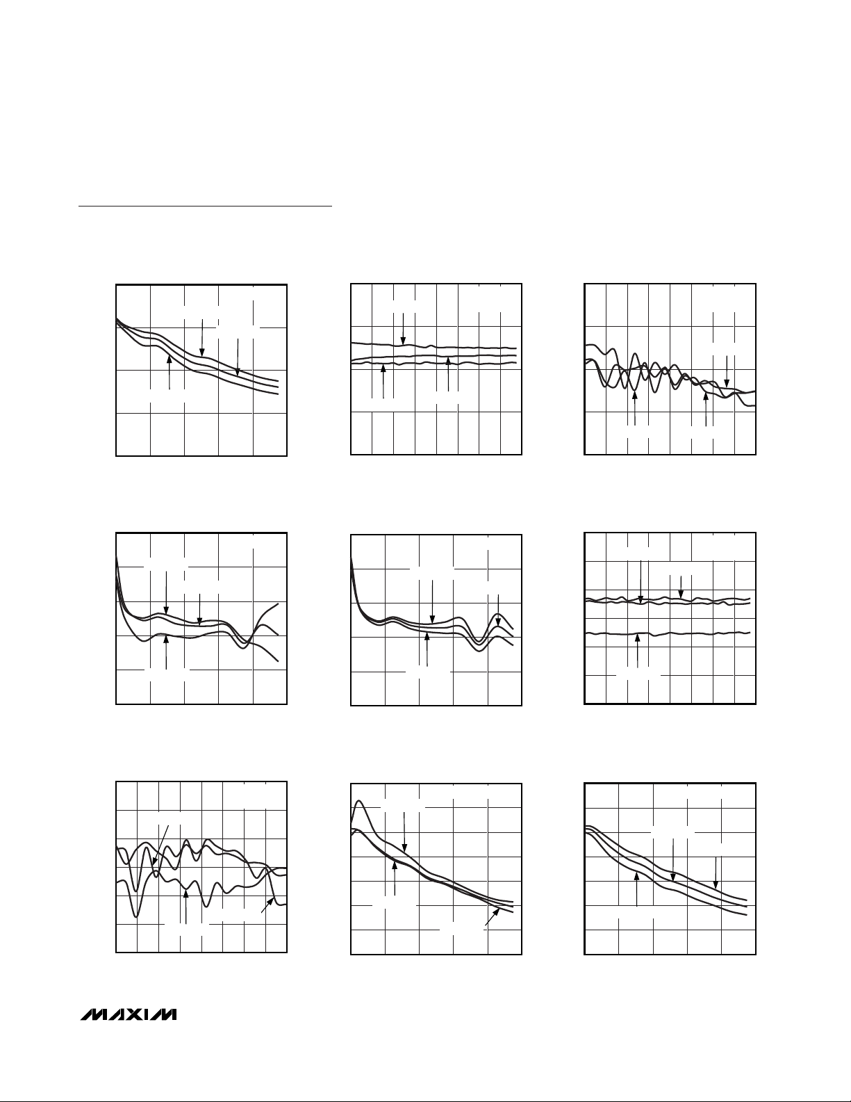
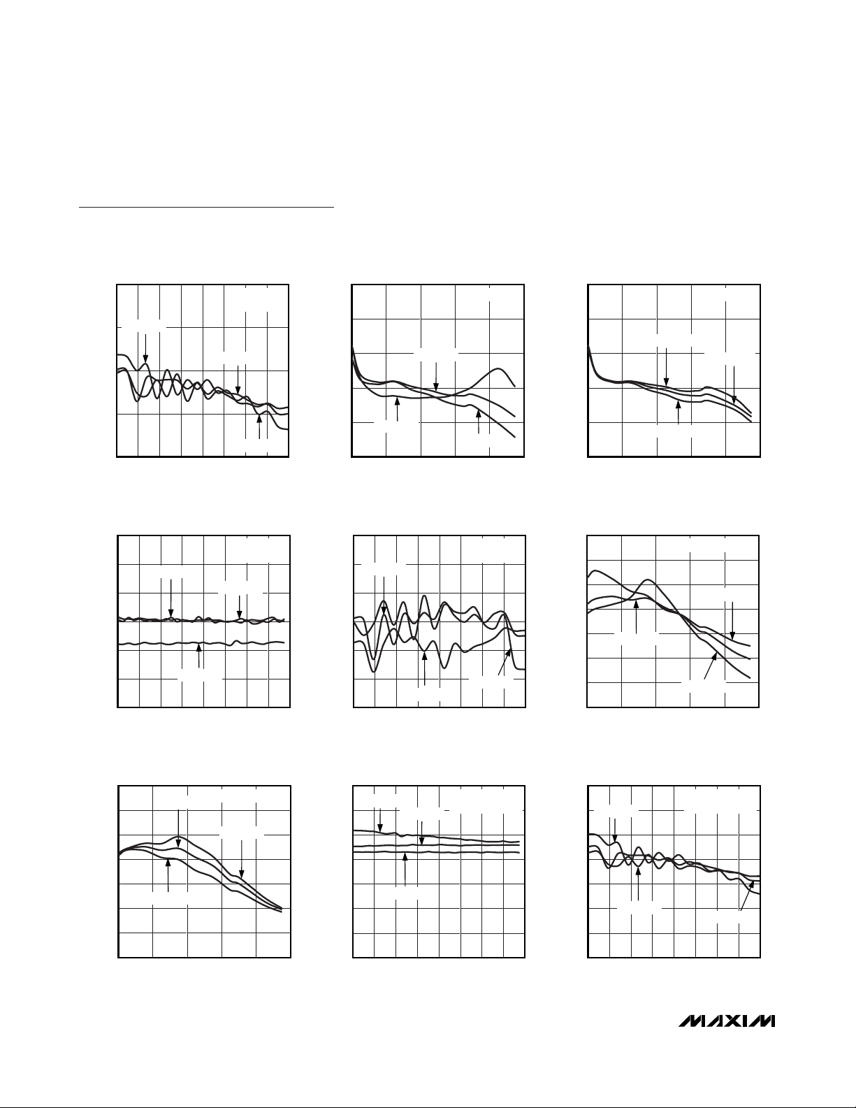
Typical Operating Characteristics
(VCC= +5.0V, HC mode, both attenuators set for maximum gain, PIN= -20dBm, fRF= 200MHz, and TC= +25°C, internal DAC reference used, unless otherwise noted.)
150
SUPPLY CURRENT vs. V
140
130
120
SUPPLY CURRENT (mA)
110
100
4.750 5.250
TC = +25°C
TC = -40°C
TC = +85°C
VCC (V)
CC
5.1255.0004.875
MAX2065 toc01
22
21
20
19
18
GAIN (dB)
17
16
15
14
GAIN vs. RF FREQUENCY
TC = -40°C
TC = +25°C
TC = +85°C
50 1050
RF FREQUENCY (MHz)
850450 650250
MAX2065 toc02
22
21
20
19
18
GAIN (dB)
17
16
15
14
GAIN vs. RF FREQUENCY
VCC = 5.25V
VCC = 5.00V
VCC = 4.75V
50 1050
RF FREQUENCY (MHz)
MAX2065 toc03
850450 650250
GAIN OVER DIGITAL ATTENUATOR
SETTING vs. RF FREQUENCY
22
12
2
GAIN (dB)
-8
-18
50 1050
RF FREQUENCY (MHz)
INPUT MATCH OVER DIGITAL ATTENUATOR
SETTING vs. RF FREQUENCY
0
-5
16dB
-10
-15
INPUT MATCH (dB)
-20
-25
-30
0 1000
0dB, 8dB
4dB
31dB
RF FREQUENCY (MHz)
1dB, 2dB
DIGITAL ATTENUATOR RELATIVE
ERROR vs. RF FREQUENCY
1.00
0.75
MAX2065 toc04
0.50
0.25
0
-0.25
RELATIVE ERROR (dB)
-0.50
-0.75
-1.00
850450 650250
50 1050
RF FREQUENCY (MHz)
850450 650250
MAX2065 toc05
OUTPUT MATCH OVER DIGITAL ATTENUATOR
SETTING vs. RF FREQUENCY
0
-5
MAX2065 toc07
-10
-15
-20
OUTPUT MATCH (dB)
-25
800400 600200
-30
0 1000
0dB, 1dB, 2dB, 4dB
8dB
16dB, 31dB
800400 600200
RF FREQUENCY (MHz)
MAX2065 toc08
DIGITAL ATTENUATOR ABSOLUTE
ERROR vs. RF FREQUENCY
1.00
0.75
0.50
0.25
0
-0.25
-0.50
-0.75
-1.00
ABSOLUTE ERROR (dB)
-1.25
-1.50
-1.70
-2.00
50 1050
RF FREQUENCY (MHz)
REVERSE ISOLATION OVER DIGITAL
ATTENUATOR SETTING vs. RF FREQUENCY
-30
-40
DIGITAL ATTENUATOR 0dB
-50
REVERSE ISOLATION (dB)
-60
-70
DIGITAL ATTENUATOR 31dB
50 1050
RF FREQUENCY (MHz)
MAX2065 toc06
850450 650250
MAX2065 toc09
850450 650250
MAX2065
50MHz to 1000MHz High-Linearity, Serial/
Parallel-Controlled Analog/Digital VGA
_______________________________________________________________________________________ 7
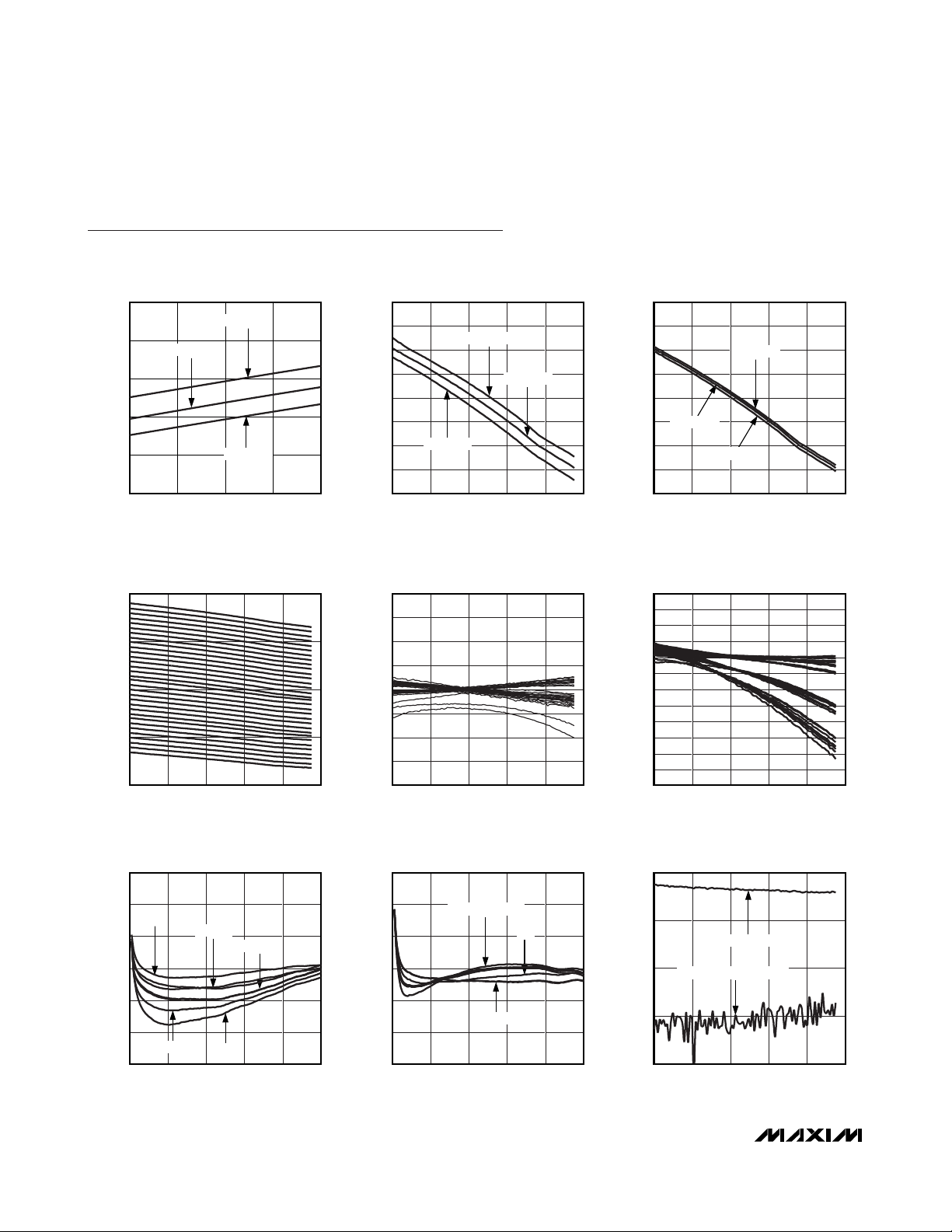
Typical Operating Characteristics (continued)
(VCC= +5.0V, HC mode, both attenuators set for maximum gain, PIN= -20dBm, fRF= 200MHz, and TC= +25°C, internal DAC reference used, unless otherwise noted.)
S21 PHASE CHANGE OVER DIGITAL
ATTENUATOR SETTING vs. RF FREQUENCY
60
50
40
30
20
10
S21 PHASE CHANGE (DEG)
0
REFERENCED TO HIGH GAIN STATE
POSITIVE PHASE = ELECTRICALLY SHORTER
-10
50 1050
RF FREQUENCY (MHz)
GAIN vs. ANALOG ATTENUATOR SETTING
22
17
12
7
2
GAIN (dB)
-3
-8
-13
-18
TC = -40°C, +25°C, +85°C
0 256
DAC CODE
RF = 200MHz
12864 96 224160 19232
MAX2065 toc10
850450 650250
MAX2065 toc13
GAIN OVER ANALOG ATTENUATOR
SETTING vs. RF FREQUENCY
22
17
12
DAC CODE 32
7
2
GAIN (dB)
-3
DAC CODE 128
-8
-13
-18
50 1050
RF FREQUENCY (MHz)
DAC CODE 0
DAC CODE 64
DAC CODE 256
GAIN vs. ANALOG ATTENUATOR SETTING
22
17
12
7
2
GAIN (dB)
-3
-8
-13
-18
0 256
VCC = 4.75V, 5.00V, 5.25V
12864 96 224160 19232
DAC CODE
850450 650250
RF = 200MHz
MAX2065 toc11
GAIN (dB)
MAX2065 toc14
INPUT MATCH (dB)
GAIN vs. ANALOG ATTENUATOR SETTING
22
17
12
7
2
1000MHz
-3
-8
-13
-18
0 256
50MHz
200MHz
450MHz
12864 96 224160 19232
DAC CODE
INPUT MATCH
vs. ANALOG ATTENUATOR SETTING
0
-5
-10
-15
-20
-25
-30
0 256
50MHz
1000MHz
200MHz
12864 96 224160 19232
DAC CODE
450MHz
MAX2065 toc12
MAX2065 toc15
OUTPUT MATCH
vs. ANALOG ATTENUATOR SETTING
0
-5
450MHz
-10
-15
-20
OUTPUT MATCH (dB)
50MHz
-25
-30
0 256
1000MHz
200MHz
12864 96 224160 19232
DAC CODE
ATTENUATOR SETTING vs. RF FREQUENCY
-30
MAX2065 toc16
-40
-50
REVERSE ISOLATION (dB)
-60
-70
REVERSE ISOLATION OVER ANALOG
DAC CODE 0
DAC CODE 255
250 450 650 850
50 1050
RF FREQUENCY (MHz)
80
70
MAX2065 toc17
60
50
40
30
20
S21 PHASE CHANGE (DEG)
10
0
-10
0 258
S21 PHASE CHANGE
vs. ANALOG ATTENUATOR SETTING
REFERENCED TO HIGH GAIN STATE
POSITIVE PHASE = ELECTRICALLY SHORTER
1000MHz
32 64 96 128 160 224192
DAC CODE
450MHz
200MHz
50MHz
MAX2065 toc18
MAX2065
50MHz to 1000MHz High-Linearity, Serial/
Parallel-Controlled Analog/Digital VGA
8 _______________________________________________________________________________________
Typical Operating Characteristics (continued)
(VCC= +5.0V, HC mode, both attenuators set for maximum gain, PIN= -20dBm, fRF= 200MHz, and TC= +25°C, internal DAC reference used, unless otherwise noted.)
NOISE FIGURE vs. RF FREQUENCY
MAX2065 toc19
RF FREQUENCY (MHz)
NOISE FIGURE (dB)
250 450 650 850
11
4
8
6
10
9
7
5
50 1050
TC = +85°C
TC = +25°C
TC = -40°C
NOISE FIGURE vs. RF FREQUENCY
MAX2065 toc20
RF FREQUENCY (MHz)
NOISE FIGURE (dB)
250 450 650 850
11
4
8
6
10
9
7
5
50 1050
VCC = 5.25V
VCC = 4.75V
VCC = 5.00V
OUTPUT P1dB vs. RF FREQUENCY
MAX2065 toc21
RF FREQUENCY (MHz)
OUTPUT P1dB (dBm)
250 450 650 850
21
15
17
20
19
18
16
50 1050
TC = -40°C
TC = +25°C
TC = +85°C
OUTPUT P1dB vs. RF FREQUENCY
MAX2065 toc22
RF FREQUENCY (MHz)
OUTPUT P1dB (dBm)
250 450 650 850
21
15
17
20
19
18
16
50 1050
VCC = 4.75V
VCC = 5.00V
VCC = 5.25V
OUTPUT IP3 vs. RF FREQUENCY
MAX2065 toc23
RF FREQUENCY (MHz)
OUTPUT IP3 (dBm)
250 450 650 850
50
30
45
40
35
50 1050
TC = -40°C
TC = +25°C
TC = +85°C
P
OUT
= 0dBm/TONE
OUTPUT IP3 vs. RF FREQUENCY
MAX2065 toc24
RF FREQUENCY (MHz)
OUTPUT IP3 (dBm)
250 450 650 850
50
30
45
40
35
50 1050
VCC = 4.75V
VCC = 5.25V
VCC = 5.00V
P
OUT
= 0dBm/TONE
OUTPUT IP3
vs. DIGITAL ATTENUATOR STATE
MAX2065 toc25
DIGITAL ATTENUATOR STATE (dB)
OUTPUT IP3 (dBm)
4 8 12 16 20 24 28
42
38
41
40
39
032
TC = +25°C LSB, USB
TC = +85°C LSB, USB
TC = -40°C LSB, USB
P
OUT
= -3dBm/TONE
RF = 200MHz
OUTPUT IP3
vs. ANALOG ATTENUATOR STATE
MAX2065 toc26
DAC CODE
OUTPUT IP3 (dBm)
32 64 96 128 160 192 224
45
25
40
35
30
0 256
TC = -40°C, +25°C, +85°C TONE = LSB, USB
P
OUT
= -3dBm/TONE
RF = 200MHz
2nd HARMONIC vs. RF FREQUENCY
MAX2065 toc27
RF FREQUENCY (MHz)
2nd HARMONIC (dBc)
250 450 650 850
80
40
70
60
50
50 1050
P
OUT
= 3dBm
TC = -40°C
TC = +25°C
TC = +85°C
MAX2065
50MHz to 1000MHz High-Linearity, Serial/
Parallel-Controlled Analog/Digital VGA
_______________________________________________________________________________________ 9
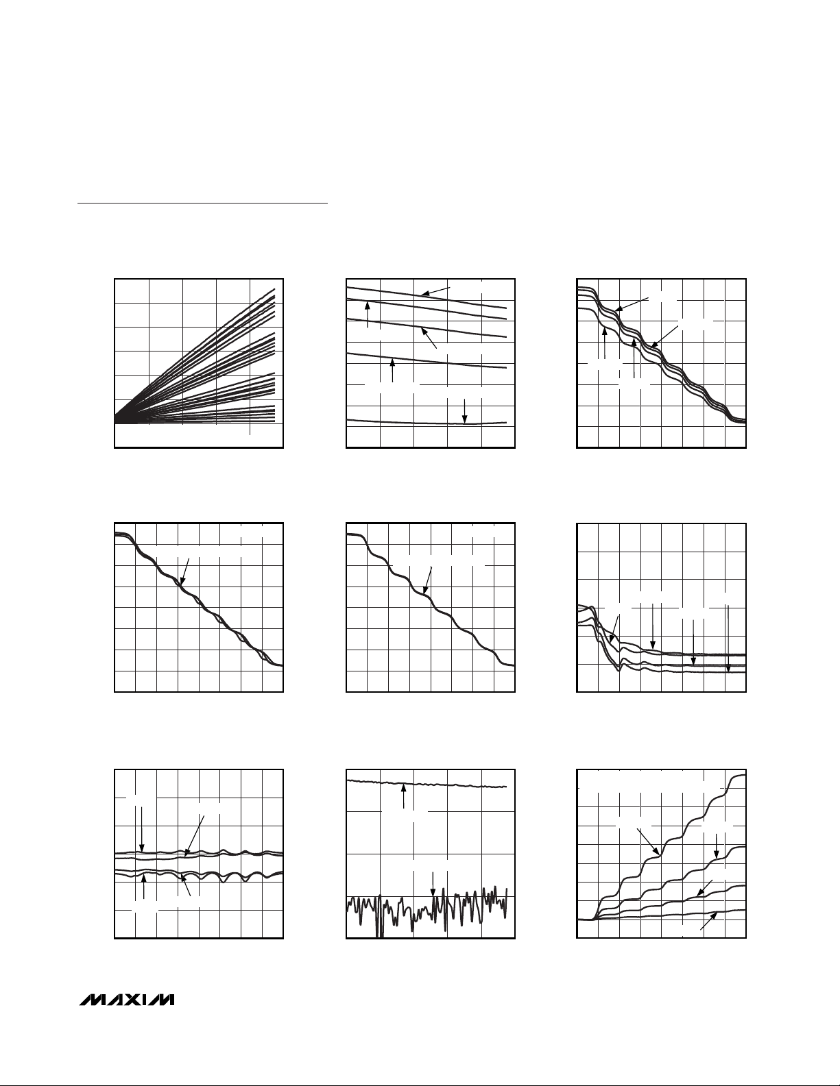
Typical Operating Characteristics (continued)
(VCC= +5.0V, HC mode, both attenuators set for maximum gain, PIN= -20dBm, fRF= 200MHz, and TC= +25°C, internal DAC reference used, unless otherwise noted.)
2nd HARMONIC
vs. ANALOG ATTENUATOR STATE
P
= 0dBm
OUT
RF = 200MHz
TC = +25°C
TC = +85°C
32 64 96 128 160 192 224
TC = -40°C
DAC CODE
3rd HARMONIC
vs. DIGITAL ATTENUATOR STATE
P
= 0dBm
OUT
TC = +25°C
TC = +85°C
TC = -40°C
RF = 200MHz
2nd HARMONIC vs. RF FREQUENCY
80
VCC = 5.25V
70
60
2nd HARMONIC (dBc)
50
40
VCC = 4.75V
250 450 650 850
50 1050
RF FREQUENCY (MHz)
VCC = 5.00V
3rd HARMONIC vs. RF FREQUENCY
110
100
90
80
3rd HARMONIC (dBc)
70
TC = +85°C
TC = +25°C
TC = -40°C
2nd HARMONIC
vs. DIGITAL ATTENUATOR STATE
MAX2065 toc28
2nd HARMONIC (dBc)
80
TC = -40°C
75
70
TC = +85°C
65
60
4 8 12 16 20 24 28
032
DIGITAL ATTENUATOR STATE (dB)
TC = +25°C
P
= 3dBm
OUT
P
= 0dBm
OUT
RF = 200MHz
MAX2065 toc29
2nd HARMONIC (dBc)
80
75
70
65
60
0 256
3rd HARMONIC vs. RF FREQUENCY
100
MAX2065 toc32
3rd HARMONIC (dBc)
95
90
85
80
75
MAX2065 toc31
3rd HARMONIC (dBc)
110
100
P
= 3dBm
OUT
VCC = 5.25V
VCC = 5.00V
90
80
70
VCC = 4.75V
P
= 3dBm
OUT
MAX2065 toc30
MAX2065 toc33
60
50 1050
250 450 650 850
RF FREQUENCY (MHz)
3rd HARMONIC
vs. ANALOG ATTENUATOR STATE
100
95
90
85
80
3rd HARMONIC (dBc)
75
70
TC = +25°C
TC = +85°C
TC = -40°C
32 64 96 128 160 192 224 256
0
DAC CODE
P
= 0dBm
OUT
RF = 200MHz
MAX2065 toc34
60
50 1050
250 450 650 850
RF FREQUENCY (MHz)
OIP2 vs. RF FREQUENCY
75
70
65
60
55
OIP2 (dBm)
50
45
40
50
TC = -40°C
TC = +25°C
250 450 650 850 1050
RF FREQUENCY (MHz)
P
OUT
TC = +85°C
= 0dBm/TONE
MAX2065 toc35
70
4 8 12 16 20 24 28 32
0
DIGITAL ATTENUATOR STATE (dB)
OIP2 vs. RF FREQUENCY
75
70
65
60
55
OIP2 (dBm)
50
45
40
VCC = 4.75V
50 1050
250 450 650 850
RF FREQUENCY (MHz)
VCC = 5.00V
P
OUT
VCC = 5.25V
= 0dBm/TONE
MAX2065 toc36

MAX2065
50MHz to 1000MHz High-Linearity, Serial/
Parallel-Controlled Analog/Digital VGA
10 ______________________________________________________________________________________
Typical Operating Characteristics (continued)
(VCC= +5.0V, HC mode, both attenuators set for maximum gain, PIN= -20dBm, fRF= 200MHz, and TC= +25°C, internal DAC reference used, unless otherwise noted.)
OIP2 vs. DIGITAL ATTENUATOR STATE
DIGITAL ATTENUATOR STATE (dB)
OIP2 (dBm)
4 8 12 2016 24 28 32
75
40
70
60
55
50
45
65
0
P
OUT
= -3dBm/TONE
TC = -40°C
TC = +85°C
TC = +25°C
MAX2065 toc37
RF = 200MHz
OIP2 vs. ANALOG ATTENUATOR STATE
DAC CODE
OIP2 (dBm)
32 64 96 160128 192 224 256
75
40
70
60
55
50
45
65
0
P
OUT
= -3dBm/TONE
TC = -40°C
TC = +85°C
TC = +25°C
MAX2065 toc38
RF = 200MHz
DAC VOLTAGE vs. DAC CODE
DAC CODE
DAC VOLTAGE (V)
32 64 96 160128 192 224 256
3.0
0
2.5
2.0
1.5
1.0
0.5
0
TC = -40°C, +25°C, +85°C
MAX2065 toc39
DAC VOLTAGE vs. DAC CODE
DAC CODE
DAC VOLTAGE (V)
32 64 96 160128 192 224 256
3.0
0
2.5
2.0
1.5
1.0
0.5
0
VCC = 4.75V, 5.00V, 5.25V
MAX2065 toc40
DAC VOLTAGE DRIFT vs. DAC CODE
DAC CODE
DAC VOLTAGE CHANGE (V)
32 64 96 160128 192 224 256
0.05
-0.05
0.04
0.01
0.02
0.03
0
-0.01
-0.02
-0.03
-0.04
0
TC CHANGED FROM +25°C TO +85°C
TC CHANGED FROM +25°C TO -40°C
MAX2065 toc41
DAC VOLTAGE DRIFT vs. DAC CODE
DAC CODE
DAC VOLTAGE CHANGE (V)
32 64 96 160128 192 224 256
0.0100
-0.0100
0.0075
0.0025
0.0050
0
-0.0025
-0.0050
-0.0075
0
VCC CHANGED FROM 5.00V TO 4.75V
VCC CHANGED FROM 5.00V TO 5.25V
MAX2065 toc42

MAX2065
50MHz to 1000MHz High-Linearity, Serial/
Parallel-Controlled Analog/Digital VGA
______________________________________________________________________________________ 11
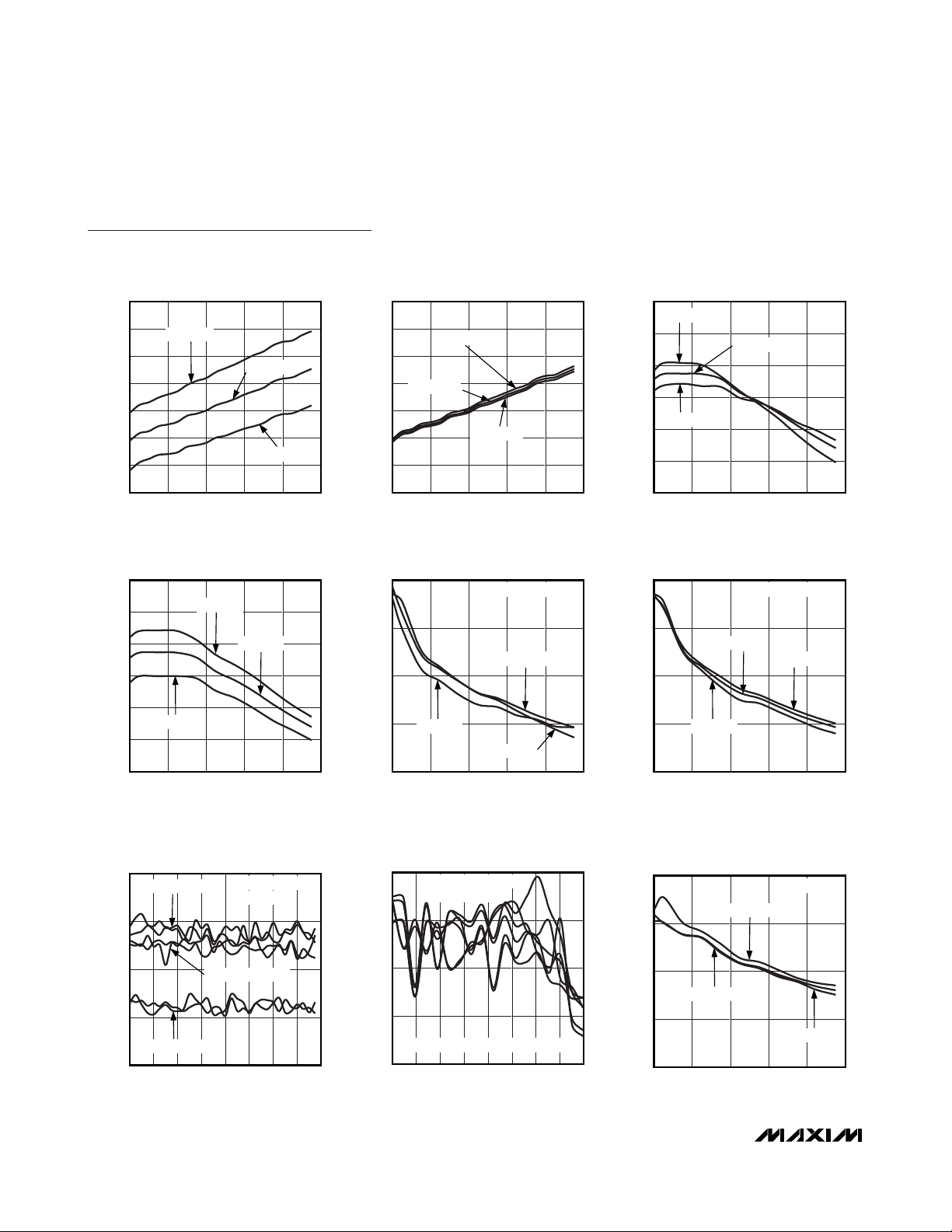
Typical Operating Characteristics (continued)
(VCC= +5.0V, attenuator only, maximum gain, PIN= -20dBm and TC= +25°C, unless otherwise noted.)
0
-1
-2
GAIN (dB)
-3
-4
-5
0
-1
GAIN vs. RF FREQUENCY
(DIGITAL ATTENUATOR ONLY)
MAXIMUM GAIN SETTING
TC = -40°C
TC = +25°C
TC = +85°C
250 450 650 850 1050
50
RF FREQUENCY (MHz)
GAIN vs. RF FREQUENCY
(ANALOG ATTENUATOR ONLY)
MAXIMUM GAIN SETTING
TC = -40°C
MAX2065 toc43
MAX2065 toc45
0
-1
-2
GAIN (dB)
-3
-4
-5
0
-1
GAIN vs. RF FREQUENCY
(DIGITAL ATTENUATOR ONLY)
MAXIMUM GAIN SETTING
VCC = 5.25V
VCC = 5.00V
50
VCC = 4.75V
250 450 650 850 1050
RF FREQUENCY (MHz)
GAIN vs. RF FREQUENCY
(ANALOG ATTENUATOR ONLY)
MAXIMUM GAIN SETTING
MAX2065 toc44
MAX2065 toc46
-2
GAIN (dB)
-3
-4
-5
TC = +85°C
50
250 450 650 850 1050
RF FREQUENCY (MHz)
TC = +25°C
-2
GAIN (dB)
-3
-4
-5
VCC = 4.75V, 5.00V, 5.25V
50
250 450 650 850 1050
RF FREQUENCY (MHz)

MAX2065
50MHz to 1000MHz High-Linearity, Serial/
Parallel-Controlled Analog/Digital VGA
12 ______________________________________________________________________________________
Typical Operating Characteristics (continued)
(VCC= +5.0V, LC mode, both attenuators set for maximum gain, PIN= -20dBm, fRF= 200MHz, and TC= +25°C, internal reference
used, unless otherwise noted.)
SUPPLY CURRENT vs. V
CC
(LOW CURRENT MODE)
VCC (V)
SUPPLY CURRENT (mA)
4.857 5.000 5.125 5.250
85
55
75
65
4.750
MAX2065 toc47
TC = -40°C
TC = +85°C
TC = +25°C
GAIN vs. RF FREQUENCY
(LOW CURRENT MODE)
RF FREQUENCY (MHz)
GAIN (dB)
250 450 650 850 1050
22
21
14
20
19
18
17
16
15
50
MAX2065 toc48
TC = -40°C
TC = +85°C
TC = +25°C
GAIN vs. RF FREQUENCY
(LOW CURRENT MODE)
RF FREQUENCY (MHz)
GAIN (dB)
250 450 650 850 1050
22
21
14
20
19
18
17
16
15
50
MAX2065 toc49
VCC = 4.75V, 5.00V, 5.25V
INPUT MATCH OVER DIGITAL ATTENUATOR
SETTING vs. RF FREQUENCY
RF FREQUENCY (MHz)
INPUT MATCH (dB)
250 450 650 850 1050
0
-5
-30
-10
-15
-20
-25
50
MAX2065 toc50
16dB
31dB
0dB, 8dB
1dB, 2dB
4dB
OUTPUT MATCH OVER DIGITAL ATTENUATOR
SETTING vs. RF FREQUENCY
RF FREQUENCY (MHz)
OUTPUT MATCH (dB)
250 450 650 850 1050
0
-5
-30
-10
-15
-20
-25
50
MAX2065 toc51
8dB
16dB, 31dB
0dB, 1dB, 2dB, 4dB
INPUT MATCH vs. ANALOG ATTENUATOR
SETTING (LOW CURRENT MODE)
DAC CODE
INPUT MATCH (dB)
32 64 96 128 160 192 224 256
0
-5
-30
-10
-15
-20
-25
0
MAX2065 toc52
200MHz
450MHz
50MHz
1000MHz
OUTPUT MATCH vs. ANALOG ATTENUATOR
SETTING (LOW CURRENT MODE)
DAC CODE
OUTPUT MATCH (dB)
32 64 96 128 160 192 224 256
0
-5
-30
-10
-15
-20
-25
0
MAX2065 toc53
50MHz
200MHz
450MHz
1000MHz
NOISE FIGURE vs. RF FREQUENCY
(LOW CURRENT MODE)
11
10
9
8
7
NOISE FIGURE (dB)
6
5
4
TC = +85°C TC = +25°C
250 450 650 850 1050
50
RF FREQUENCY (MHz)
TC = -40°C
MAX2065 toc54
NOISE FIGURE (dB)
NOISE FIGURE vs. RF FREQUENCY
(LOW CURRENT MODE)
11
10
9
8
7
6
5
4
VCC = 4.75V, 5.00V, 5.25V
250 450 650 850 1050
50
RF FREQUENCY (MHz)
MAX2065 toc55

MAX2065
50MHz to 1000MHz High-Linearity, Serial/
Parallel-Controlled Analog/Digital VGA
______________________________________________________________________________________ 13
Typical Operating Characteristics (continued)
(VCC= +5.0V, LC mode, both attenuators set for maximum gain, PIN= -20dBm, fRF= 200MHz, and TC= +25°C, internal reference
used, unless otherwise noted.)
OUTPUT P1dB vs. RF FREQUENCY
(LOW CURRENT MODE)
18
TC = -40°C
17
16
15
OUTPUT P1dB (dBm)
14
13
TC = +85°C
250 450 650 850 1050
50
RF FREQUENCY (MHz)
OUTPUT IP3 vs. RF FREQUENCY
(LOW CURRENT MODE)
45
40
VCC = 5.00V
TC = +25°C
VCC = 5.25V
MAX2065 toc56
OUTPUT P1dB (dBm)
MAX2065 toc59
OUTPUT P1dB vs. RF FREQUENCY
(LOW CURRENT MODE)
18
17
16
15
14
13
VCC = 5.25V
250 450 650 850 1050
50
VCC = 5.00V
RF FREQUENCY (MHz)
VCC = 4.75V
OUTPUT IP3 vs. DIGITAL ATTENUATOR
STATE (LOW CURRENT MODE)
45
TC = +25°C LSB, USB
40
P
= -3dBm/TONE
OUT
RF = 200MHz
MAX2065 toc57
OUTPUT IP3 (dBm)
MAX2065 toc60
OUTPUT IP3 vs. RF FREQUENCY
(LOW CURRENT MODE)
45
40
35
30
25
50
TC = +25°C
TC = -40°C
TC = +85°C
250 450 650 850 1050
RF FREQUENCY (MHz)
OUTPUT IP3 vs. ANALOG ATTENUATOR
STATE (LOW CURRENT MODE)
45
P
= -3dBm/TONE
OUT
RF = 200MHz
40
MAX2065 toc58
MAX2065 toc61
35
OUTPUT IP3 (dBm)
30
25
VCC = 4.75V
250 450 650 850 1050
50
RF FREQUENCY (MHz)
2nd HARMONIC vs. RF FREQUENCY
(LOW CURRENT MODE)
80
70
60
2nd HARMONIC (dBc)
50
40
250 450 650 850 1050
50
RF FREQUENCY (MHz)
TC = +25°C
P
= 3dBm
OUT
TC = -40°C
TC = +85°C
OUTPUT IP3 (dBm)
MAX2065 toc62
2nd HARMONIC (dBc)
35
TC = -40°C LSB, USB
30
25
4 8 12 16 20 24 28 32
0
DIGITAL ATTENUATOR STATE (dB)
TC = +85°C LSB, USB
2nd HARMONIC vs. RF FREQUENCY
(LOW CURRENT MODE)
80
VCC = 5.00V
70
60
VCC = 4.75V
50
40
250 450 650 850 1050
50
RF FREQUENCY (MHz)
P
= 3dBm
OUT
VCC = 5.25V
OUTPUT IP3 (dBm)
MAX2065 toc63
2nd HARMONIC (dBc)
35
30
25
TC = -40°C, +25°C, +85°C
TONE = LSB, USB
32 64 98 128 160 192 224 256
0
DAC CODE
2nd HARMONIC vs. DIGITAL ATTENUATOR
STATE (LOW CURRENT MODE)
80
75
70
65
60
TC = -40°C
TC = +85°C
TC = +25°C
0
4 8 12 2016 24 28 32
DIGITAL ATTENUATOR STATE (dB)
P
= 0dBm
OUT
RF = 200MHz
MAX2065 toc64
MAX2065
50MHz to 1000MHz High-Linearity, Serial/
Parallel-Controlled Analog/Digital VGA
14 ______________________________________________________________________________________
Typical Operating Characteristics (continued)
(VCC= +5.0V, LC mode, both attenuators set for maximum gain, PIN= -20dBm, fRF= 200MHz, and TC= +25°C, internal reference
used, unless otherwise noted.)
2nd HARMONIC vs. ANALOG ATTENUATOR
STATE (LOW CURRENT MODE)
DAC CODE
2nd HARMONIC (dBc)
32 64 96 160128 192 224 256
80
60
75
70
65
0
MAX2065 toc65
TC = +85°C
TC = -40°C
TC = +25°C
P
OUT
= 0dBm
RF = 200MHz
3rd HARMONIC vs. RF FREQUENCY
(LOW CURRENT MODE)
RF FREQUENCY (MHz)
3rd HARMONIC (dBc)
250 450 650 850 1050
110
60
100
90
80
70
50
MAX2065 toc66
TC = +85°C
TC = -40°C
TC = +25°C
P
OUT
= 3dBm
OIP2 vs. RF FREQUENCY
(LOW CURRENT MODE)
RF FREQUENCY (MHz)
OIP2 (dBm)
250 450 650 850 1050
75
40
70
65
60
45
50
55
50
MAX2065 toc71
VCC = 5.25V
VCC = 5.00V
VCC = 4.75V
P
OUT
= 0dBm/TONE
OIP2 vs. DIGITAL ATTENUATOR
STATE (LOW CURRENT MODE)
DIGITAL ATTENUATOR STATE (dB)
OIP2 (dBm)
84121620242832
75
40
70
65
60
45
50
55
0
MAX2065 toc72
P
OUT
= -3dBm/TONE
RF = 200MHz
TC = +85°C
TC = -40°C
TC = +25°C
OIP2 vs. ANALOG ATTENUATOR
STATE (LOW CURRENT MODE)
DAC CODE
OIP2 (dBm)
6432 96 128 160 192 224 256
75
40
70
65
60
45
50
55
0
MAX2065 toc73
P
OUT
= -3dBm/TONE
RF = 200MHz
TC = +85°C
TC = -40°C
TC = +25°C
3rd HARMONIC vs. RF FREQUENCY
(LOW CURRENT MODE)
RF FREQUENCY (MHz)
3rd HARMONIC (dBc)
250 450 650 850 1050
110
60
100
90
80
70
50
MAX2065 toc67
VCC = 5.25V
VCC = 5.00V
VCC = 4.75V
P
OUT
= 3dBm
3rd HARMONIC vs. DIGITAL ATTENUATOR
STATE (LOW CURRENT MODE)
DIGITAL ATTENUATOR STATE (dB)
3rd HARMONIC (dBc)
4 8 12 16 20 24 28 32
100
70
95
90
85
75
80
0
MAX2065 toc68
TC = +25°C
TC = +85°C
TC = -40°C
P
OUT
= 0dBm
RF = 200MHz
3rd HARMONIC vs. ANALOG ATTENUATOR
STATE (LOW CURRENT MODE)
DAC CODE
3rd HARMONIC (dBc)
32 64 96 128 160 192 224 256
100
70
95
90
85
75
80
0
MAX2065 toc69
TC = +25°C
TC = +85°C
TC = -40°C
P
OUT
= 0dBm
RF = 200MHz
OIP2 vs. RF FREQUENCY
(LOW CURRENT MODE)
RF FREQUENCY (MHz)
OIP2 (dBm)
250 450 650 850 1050
75
40
70
65
60
45
50
55
50
MAX2065 toc70
TC = +25°C
TC = +85°C
TC = -40°C
P
OUT
= 0dBm/TONE

MAX2065
Typical Operating Characteristics (continued)
(VCC= +3.3V, HC mode, both attenuators set for maximum gain, PIN= -20dBm, fRF= 200MHz, and TC= +25°C, internal DAC reference used, unless otherwise noted.)
GAIN vs. RF FREQUENCY
RF FREQUENCY (MHz)
GAIN (dB)
250 450 650 850 1050
21
13
18
17
19
20
16
15
14
50
MAX2065 toc75
TC = +85°C
TC = -40°C
VCC = 3.3V
TC = +25°C
GAIN vs. RF FREQUENCY
RF FREQUENCY (MHz)
GAIN (dB)
250 450 650 850 1050
21
13
18
17
19
20
16
15
14
50
MAX2065 toc76
VCC = 3.6V
VCC = 3.3V
VCC = 3.0V
INPUT MATCH OVER DIGITAL ATTENUATOR
SETTING vs. RF FREQUENCY
RF FREQUENCY (MHz)
INPUT MATCH (dB)
250 450 650 850 1050
0
-30
-10
-15
-5
-20
-25
50
MAX2065 toc77
16dB
4dB
0dB, 8dB
1dB, 2dB
VCC = 3.3V
31dB
OUTPUT MATCH OVER DIGITAL ATTENUATOR
SETTING vs. RF FREQUENCY
RF FREQUENCY (MHz)
OUTPUT MATCH (dB)
200 400 600 800 1000
0
-30
-10
-15
-5
-20
-25
0
MAX2065 toc78
16dB, 31dB
0dB, 1dB, 2dB, 4dB
VCC = 3.3V
8dB
INPUT MATCH
vs. ANALOG ATTENUATOR SETTING
DAC CODE
INPUT MATCH (dB)
32 64 96 128 160 192 224 256
0
-30
-10
-15
-5
-20
-25
0
MAX2065 toc79
1000MHz
200MHz
450MHz
50MHz
VCC = 3.3V
OUTPUT MATCH
vs. ANALOG ATTENUATOR SETTING
DAC CODE
OUTPUT MATCH (dB)
32 64 96 128 160 192 224 256
0
-30
-10
-15
-5
-20
-25
0
MAX2065 toc80
1000MHz
200MHz
450MHz
50MHz
VCC = 3.3V
NOISE FIGURE vs. RF FREQUENCY
RF FREQUENCY (MHz)
NOISE FIGURE (dB)
250 450 650 850 1050
11
4
9
8
7
10
6
5
50
MAX2065 toc81
VCC = 3.3V
TC = +85°C
TC = +25°C
TC = -40°C
NOISE FIGURE vs. RF FREQUENCY
RF FREQUENCY (MHz)
NOISE FIGURE (dB)
250 450 650 850
11
4
9
8
7
10
6
5
50
MAX2065 toc82
VCC = 3.3V
VCC = 3.0V
VCC = 3.6V
SUPPLY CURRENT vs. V
CC
V
CC
(V)
SUPPLY CURRENT (mA)
3.15 3.30 3.45 3.60
75
45
65
55
3.00
MAX2065 toc74
TC = +85°C
TC = -40°C
TC = +25°C
50MHz to 1000MHz High-Linearity, Serial/
Parallel-Controlled Analog/Digital VGA
______________________________________________________________________________________ 15

MAX2065
50MHz to 1000MHz High-Linearity, Serial/
Parallel-Controlled Analog/Digital VGA
16 ______________________________________________________________________________________
Typical Operating Characteristics (continued)
(VCC= +3.3V, HC mode, both attenuators set for maximum gain, PIN= -20dBm, fRF= 200MHz, and TC= +25°C, internal DAC reference used, unless otherwise noted.)
OUTPUT P1dB vs. RF FREQUENCY
RF FREQUENCY (MHz)
OUTPUT P1dB (dBm)
250 450 650 850 1050
17
9
10
15
14
13
16
12
11
50
MAX2065 toc83
TC = +85°C
TC = +25°C
VCC = 3.3V
TC = -40°C
OUTPUT P1dB vs. RF FREQUENCY
17
16
15
14
13
12
OUTPUT P1dB (dBm)
11
10
9
VCC = 3.3V
VCC = 3.0V
250 450 650 850 1050
50
RF FREQUENCY (MHz)
VCC = 3.6V
MAX2065 toc84
OUTPUT IP3 (dBm)
OUTPUT IP3 vs. RF FREQUENCY
50
45
40
35
30
25
20
250 450 650 850 1050
50
RF FREQUENCY (MHz)
VCC = 3.3V
TC = +25°C
TC = +85°C
MAX2065 toc85
TC = -40°C
50
45
40
35
OUTPUT IP3 (dBm)
30
25
20
80
70
60
50
2nd HARMONIC (dBc)
40
30
OUTPUT IP3 vs. RF FREQUENCY
VCC = 3.3V
VCC = 3.6V
VCC = 3.0V
250 450 650 850 1050
50
RF FREQUENCY (MHz)
2nd HARMONIC vs. RF FREQUENCY
P
OUT
TC = +25°C
TC = -40°C
250 450 650 850 1050
50
RF FREQUENCY (MHz)
VCC = 3.3V
TC = +85°C
= 3dBm
MAX2065 toc86
OUTPUT IP3 (dBm)
MAX2065 toc89
2nd HARMONIC (dBc)
vs. DIGITAL ATTENUATOR STATE
OUTPUT IP3
39
VCC = 3.3V
38
37
36
35
34
TC = -40°C, +25°C, +85°C
TONE = LSB, USB
4 8 12 16 20 24 28 32
0
DIGITAL ATTENUATOR STATE (dB)
P
2nd HARMONIC vs. RF FREQUENCY
80
70
60
50
40
30
VCC = 3.3V
VCC = 3.6V
VCC = 3.0V
250 450 650 850 1050
50
RF FREQUENCY (MHz)
= -3dBm/TONE
OUT
RF = 200MHz
P
OUT
= 3dBm
MAX2065 toc87
OUTPUT IP3 (dBm)
MAX2065 toc90
2nd HARMONIC (dBc)
vs. ANALOG ATTENUATOR STATE
OUTPUT IP3
45
VCC = 3.3V
40
35
30
25
TC = -40°C, +25°C, +85°C
TONE = LSB, USB
32 64 96 128 160 192 224 256
0
DAC CODE
2nd HARMONIC
vs. DIGITAL ATTENUATOR STATE
70
TC = +85°C
65
60
55
TC = -40°C
50
4 8 12 16 20 24 28 32
0
DIGITAL ATTENUATOR STATE (dB)
P
= -3dBm/TONE
OUT
RF = 200MHz
P
RF = 200MHz
VCC = 3.3V
TC = +25°C
OUT
MAX2065 toc88
= 0dBm
MAX2065 toc91

MAX2065
50MHz to 1000MHz High-Linearity, Serial/
Parallel-Controlled Analog/Digital VGA
______________________________________________________________________________________ 17
Typical Operating Characteristics (continued)
(VCC= +3.3V, HC mode, both attenuators set for maximum gain, PIN= -20dBm, fRF= 200MHz, and TC= +25°C, internal DAC reference used, unless otherwise noted.)
3rd HARMONIC vs. RF FREQUENCY
RF FREQUENCY (MHz)
3rd HARMONIC (dBc)
250 450 650 850 1050
110
50
100
90
80
70
60
50
MAX2065 toc93
TC = -40°C
P
OUT
= 3dBm
TC = +85°C
TC = +25°C
VCC = 3.3V
3rd HARMONIC vs. RF FREQUENCY
RF FREQUENCY (MHz)
3rd HARMONIC (dBc)
250 450 650 850 1050
110
50
100
90
80
70
60
50
MAX2065 toc94
P
OUT
= 3dBm
VCC = 3.3V
VCC = 3.6V
VCC = 3.0V
3rd HARMONIC
vs. DIGITAL ATTENUATOR STATE
DIGITAL ATTENUATOR STATE (dB)
3rd HARMONIC (dBc)
4 8 12 16 20 24 28 32
90
70
85
80
75
0
MAX2065 toc95
TC = -40°C
P
OUT
= 0dBm
TC = +25°C, +85°C
VCC = 3.3V
RF = 200MHz
3rd HARMONIC
vs. ANALOG ATTENUATOR STATE
DAC CODE
3rd HARMONIC (dBc)
32 64 96 128 160 192 224 256
110
50
100
90
80
70
60
0
MAX2065 toc96
TC = -40°C
P
OUT
= 0dBm
TC = +85°C
TC = +25°C
VCC = 3.3V
RF = 200MHz
OIP2 vs. RF FREQUENCY
RF FREQUENCY (MHz)
OIP2 (dBm)
250 450 650 850 1050
70
30
60
50
40
50
MAX2065 toc97
TC = -40°C
P
OUT
= 0dBm/TONE
TC = +85°C
TC = +25°C
VCC = 3.3V
OIP2 vs. RF FREQUENCY
RF FREQUENCY (MHz)
OIP2 (dBm)
250 450 650 850 1050
70
30
60
50
40
50
MAX2065 toc98
P
OUT
= 0dBm/TONE
VCC = 3.3V
VCC = 3.6V
VCC = 3.0V
OIP2 vs. DIGITAL ATTENUATOR STATE
DIGITAL ATTENUATOR STATE (dB)
OIP2 (dBm)
4 8 12 16 20 24 28 32
70
30
60
50
40
0
MAX2065 toc99
TC = -40°C
TC = +25°C
P
OUT
= 0dBm/TONE
TC = +85°C
VCC = 3.3V
RF = 200MHz
OIP2 vs. ANALOG ATTENUATOR STATE
DAC CODE
OIP2 (dBm)
32 64 96 128 160 192 224 256
70
30
60
50
40
0
MAX2065 toc100
TC = -40°C
TC = +25°C
P
OUT
= -3dBm/TONE
TC = +85°C
VCC = 3.3V
RF = 200MHz
2nd HARMONIC
vs. ANALOG ATTENUATOR STATE
DAC CODE
2nd HARMONIC (dBc)
32 64 96 128 160 192 224 256
80
30
70
60
50
40
0
MAX2065 toc92
TC = -40°C
P
OUT
= 0dBm
TC = +85°C
TC = +25°C
VCC = 3.3V
RF = 200MHz

MAX2065
50MHz to 1000MHz High-Linearity, Serial/
Parallel-Controlled Analog/Digital VGA
18 ______________________________________________________________________________________
Pin Description
PIN NAME DESCRIPTION
1, 16, 19, 22,
24–28, 30,
31, 33–36
2 VREF_SELECT
3 VDAC_EN DAC Enable/Disable Logic Input. Logic 0 = disable DAC circuit, Logic 1 = enable DAC circuit.
4 DATA SPI Data Digital Input
5 CLK SPI Clock Digital Input
6 CS SPI Chip-Select Digital Input
7 VDD_LOGIC Digital Logic Supply Input
8 SER/PAR
9 STATE_A Digital Attenuator Preprogrammed Attenuation State Logic Input
10 STATE_B
11 D4 16dB Attenuator Logic Input. Logic 0 = disable, Logic 1 = enable.
12 D3 8dB Attenuator Logic Input. Logic 0 = disable, Logic 1 = enable.
13 D2 4dB Attenuator Logic Input. Logic 0 = disable, Logic 1 = enable.
14 D1 2dB Attenuator Logic Input. Logic 0 = disable, Logic 1 = enable.
15 D0 1dB Attenuator Logic Input. Logic 0 = disable, Logic 1 = enable.
17 AMP_OUT Driver Amplifier Output (50Ω)
18 RSET Driver Amplifier Bias-Setting. See the External Bias section.
20 AMP_IN Driver Amplifier Input (50Ω)
21 VC C _AMP Driver Amplifier Supply Voltage Input
23 ATTEN2_OUT 5-Bit Digital Attenuator Output (50Ω)
29 ATTEN2_IN 5-Bit Digital Attenuator Input (50Ω)
32 ATTEN1_OUT Analog Attenuator Output (50Ω)
37 ATTEN1_IN Analog Attenuator Input (50Ω)
38 VC C _ANALOG Analog Bias and Control Supply Voltage Input
39 AN ALOG_V C TRL Analog Attenuator Voltage Control Input
40 VREF_IN External DAC Voltage Reference Input
—EP
GND Ground
DAC Reference Voltage Selection Logic Input. Logic 1 = internal DAC reference voltage,
Log i c 0 = exter nal D AC r efer ence vol tag e. Log i c i np ut d i sab l ed ( d on’ t car e) w hen V D AC _E N = Log i c 0.
Digital Attenuator SPI or Parallel Control Selection Logic Input. Logic 0 = parallel control,
Logic 1 = serial control.
State A State B Digital Attenuator
Logic = 0 Logic = 0 Preprogrammed State 1
Logic = 1 Logic = 0 Preprogrammed State 2
Logic = 0 Logic = 1 Preprogrammed State 3
Logic = 1 Logic = 1 Preprogrammed State 4
E xp osed P ad . Inter nal l y connected to GN D . C onnect E P to GN D for p r op er RF p er for m ance and
enhanced ther m al d i ssi p ati on.

MAX2065
50MHz to 1000MHz High-Linearity, Serial/
Parallel-Controlled Analog/Digital VGA
______________________________________________________________________________________ 19
Detailed Description
The MAX2065 high-linearity analog/digital variable-gain
amplifier is a general-purpose, high-performance
amplifier designed to interface with 50Ω systems operating in the 50MHz to 1000MHz frequency range.
The MAX2065 integrates one digital attenuator and one
analog attenuator to provide 62dB of total gain control,
as well as a driver amplifier optimized to provide high
gain, high IP3, low noise figure, and low power consumption. For applications that do not require high linearity, the
bias current of the amplifier can be adjusted by an external resistor to further reduce power consumption.
The digital attenuator is controlled as a slave peripheral
using either the SPI-compatible interface or a parallel
bus with 31dB total adjustment range in 1dB steps. An
added feature allows “rapid-fire” gain selection
between each of the four unique steps (preprogrammed by the user through the SPI-compatible interface). The 2-pin control allows the user to quickly
access any one of four customized attenuation states
without reprogramming the SPI bus. The analog attenuator is controlled using an external voltage or through
the SPI-compatible interface using an on-chip DAC.
Because each of the three stages has its own external
RF input and RF output, this component can be configured to either optimize NF (amplifier configured first),
OIP3 (amplifier last), or a compromise of NF and OIP3.
The device’s performance features include 22dB standalone amplifier gain (amplifier only), 6.5dB NF at maximum gain (includes attenuator insertion loss for both
attenuators), and a high OIP3 level of +42dBm. Each of
these features makes the MAX2065 an ideal VGA for
numerous receiver and transmitter applications.
In addition, the MAX2065 operates from a single +5V
supply, or a single +3.3V supply with slightly reduced
performance, and has adjustable bias to trade current
consumption for linearity performance.
Analog and 5-Bit Digital
Attenuator Control
The MAX2065 integrates one analog attenuator and
one 5-bit digital attenuator to achieve a high level of
dynamic range. The analog attenuator has a 31dB
range and is controlled using an external voltage or
through the 3-wire serial peripheral interface (SPI) using
an on-chip 8-bit DAC. The digital attenuator has a 31dB
control range, a 1dB step size, and is programmed
through the 3-wire SPI. See the
Applications Information
section and Table 1 for attenuator programming details.
The attenuators can be used for both static and dynamic power control.
Driver Amplifier
The MAX2065 includes a high-performance driver with
a fixed gain of 22dB. The driver amplifier circuit is optimized for high linearity for the 50MHz to 1000MHz frequency range.
Applications Information
SPI Interface and Attenuator Settings
The digital attenuator is programmed through the 3-wire
SPI/MICROWIRE™-compatible serial interface using
5-bit words. Twenty-eight bits of data are shifted in MSB
first and is framed by CS. When CS is low, the clock is
active and data is shifted on the rising edge of the
clock. When CS transitions high, the data is latched
and the attenuator setting changes (Figure 1). See
Table 2 for details on the SPI data format.
Table 1. Control Logic
X = Don’t care.
MICROWIRE is a trademark of National Semiconductor Corp.
VDAC_EN SER/PAR VR EF _ SEL EC T
00X
101
01X
110
ATTENUATOR
Controlled by external
control voltage
Controlled by on-chip
DAC
Controlled by external
control voltage
Controlled by on-chip
DAC
ANALOG
DIGITAL
ATTENUATOR
Parallel controlled Disabled
Parallel controlled
SPI controlled Disabled
SPI controlled
D/A CONVERTER
Enabled (DAC uses onchip voltage reference)
Enabled (DAC uses
external voltage
reference)

MAX2065
50MHz to 1000MHz High-Linearity, Serial/
Parallel-Controlled Analog/Digital VGA
20 ______________________________________________________________________________________
Figure 1. MAX2065 SPI Timing Diagram
Table 2. SPI Data Format
MSB LSB
DATA
CLOCK
CS
t
EWS
FUNCTION BIT DESCRIPTION
D27 (MSB) 16dB step (MSB of the 5-bit word used to program the digital attenuator state 4)
Digital Attenuator State 4
Digital Attenuator State 3
Digital Attenuator State 2
Digital Attenuator State 1
DN
D26 8dB step
D25 4dB step
D24 2dB step
D23 1dB step (LSB)
D22
D21
D20
D19
D18
D17
D16
D15
D14
D13
D12
D11
D10
D9
D8
D(N-1) D1 D0
t
CS
5-bit word used to program the digital attenuator state 3 (see the description for digital
attenuator state 4)
5-bit word used to program the digital attenuator state 2 (see the description for digital
attenuator state 4)
5-bit word used to program the digital attenuator state 1 (see the description for digital
attenuator state 4)
t
t
CH
CW
t
ES
t
EW

MAX2065
50MHz to 1000MHz High-Linearity, Serial/
Parallel-Controlled Analog/Digital VGA
______________________________________________________________________________________ 21
Table 2. SPI Data Format (continued)
Attenuator and DAC Operation
The analog attenuator is controlled by an external control voltage applied at ANALOG_VCTRL (pin 39) or by
the on-chip 8-bit DAC, while the digital attenuator is controlled through the SPI-compatible interface or parallel
bus. The DAC enable/disable logic-input pin
(VDAC_EN), digital attenuator SPI or parallel control
selection logic-input pin (SER/PAR), and the DAC reference voltage selection logic-input pin (VREF_SELECT)
determine how the attenuators are controlled. The onchip DAC can also be enabled or disabled. When the
DAC is enabled, either the on-chip voltage reference or
the external voltage reference can be selected. See
Table 1 for the attenuator and DAC operation truth table.
Digital Attenuator Settings
Using the Parallel Control Bus
To capitalize on its fast 25ns switching capability, the
MAX2065 offers a supplemental 5-bit parallel control
interface. The digital logic attenuator-control pins
(D0–D4) enable the attenuator stages (Table 3).
Direct access to this 5-bit bus enables the user to avoid
any programming delays associated with the SPI
interface. One of the limitations of any SPI bus is the
speed at which commands can be clocked into each
peripheral device. By offering direct access to the 5-bit
parallel interface, the user can quickly shift between
digital attenuator states needed for critical “fast-attack”
automatic gain control (AGC) applications.
“Rapid-Fire” Preprogrammed
Attenuation States
The MAX2065 has an added feature that provides
“rapid fire” gain selection between four preprogrammed attenuation steps. As with the supplemental
5-bit bus mentioned above, this “rapid fire” gain selection allows the user to quickly access any one of four
customized digital attenuation states without incurring
the delays associated with reprogramming the device
through the SPI bus.
The switching speed is comparable to that achieved
using the supplemental 5-bit parallel bus. However, by
employing this specific feature, the digital attenuator
I/O is further reduced by a factor of either 5 or 2.5 (5
control bits vs. 1 or 2, respectively) depending on the
number of states desired.
Table 3. Digital Attenuator Settings (Parallel Control)
FUNCTION BIT DESCRIPTION
D7 Bit 7 (MSB) of on-chip DAC used to program the analog attenuator
D6 Bit 6 of DAC
D5 Bit 5 of DAC
On-Chip DAC
D4 Bit 4 of DAC
D3 Bit 3 of DAC
D2 Bit 2 of DAC
D1 Bit 1 of DAC
D0 (LSB) Bit 0 (LSB) of the on-chip DAC
INPUT LOGIC = 0 (OR GROUND) LOGIC = 1
D0 Disable 1dB attenuator, or when SPI is default programmer Enable 1dB attenuator
D1 Disable 2dB attenuator, or when SPI is default programmer Enable 2dB attenuator
D2 Disable 4dB attenuator, or when SPI is default programmer Enable 4dB attenuator
D3 Disable 8dB attenuator, or when SPI is default programmer Enable 8dB attenuator
D4 Disable 16dB attenuator, or when SPI is default programmer Enable 16dB attenuator

MAX2065
50MHz to 1000MHz High-Linearity, Serial/
Parallel-Controlled Analog/Digital VGA
22 ______________________________________________________________________________________
The user can employ the STATE_A and STATE_B logicinput pins to apply each step as required (Table 4).
Toggling just the STATE_A pin (one control bit) yields
two preprogrammed attenuation states; toggling both
the STATE_A and STATE_B pins together (two control
bits) yield four preprogrammed attenuation states.
As an example, assume that the AGC application
requires a static attenuation adjustment to trim out gain
inconsistencies within a receiver lineup. The same AGC
circuit can also be called upon to dynamically attenuate
an unwanted blocker signal that could de-sense the
receiver and lead to an ADC overdrive condition. In this
example, the MAX2065 would be preprogrammed
(through the SPI bus) with two customized attenuation
states—one to address the static gain trim adjustment,
the second to counter the unwanted blocker condition.
Toggling just the STATE_A control bit enables the user
to switch quickly between the static and dynamic attenuation settings with only one I/O pin.
If desired, the user can also program two additional
attenuation states by using the STATE_B control bit as
a second I/O pin. These two additional attenuation settings are useful for software-defined radio applications
where multiple static gain settings may be needed to
account for different frequencies of operation, or where
multiple dynamic attenuation settings are needed to
account for different blocker levels (as defined by multiple wireless standards).
Cascaded OIP3 Considerations
Due to both attenuator’s finite IP3 performance, the
cascaded OIP3 degrades when both attenuators are
set at higher attenuation states.
External Bias
Bias currents for the driver amplifier are set and optimized through external resistors. Resistors R1 and R1A
connected to RSET (pin 18) set the bias current for the
amplifier. The external biasing resistor values can be
increased for reduced current operation at the expense
of performance.
Table 4. Preprogrammed Attenuation
State Settings
Table 5. Typical Application Circuit Component Values (HC Mode)
STATE_A STATE_B DIGITAL ATTENUATOR
0 0 Preprogrammed attenuation state 1
1 0 Preprogrammed attenuation state 2
0 1 Preprogrammed attenuation state 3
1 1 Preprogrammed attenuation state 4
DESIGNATION VALUE SIZE VENDOR DESCRIPTION
C1, C2, C7, C11 10nF 0402 Murata Mfg. Co., Ltd. X7R
C3, C4, C6, C8, C9, C10 1000pF 0402 Murata Mfg. Co., Ltd. C0G ceramic capacitor
C12, C13 150pF 0402 Murata Mfg. Co., Ltd. C0G ceramic capacitor
L1 470nH 1008 Coilcraft, Inc. 1008CS-471XJLC
R1, R1A 10Ω 0402 Panasonic Corp. 1%
R2 (+3.3V applications only) 1kΩ 0402 Panasonic Corp. 1%
R3 (+3.3V applications only) 2kΩ 0402 Panasonic Corp. 1%
R4 (+5V applications and
using internal DAC only)
U1 —
47kΩ 0402 Panasonic Corp. 1%
40-pin thin QFN-EP
(6mm x 6mm)
Maxim Integrated
Products, Inc.
MAX2065ETL+

MAX2065
50MHz to 1000MHz High-Linearity, Serial/
Parallel-Controlled Analog/Digital VGA
______________________________________________________________________________________ 23
+5V and +3.3V Supply Voltage
The MAX2065 features an optional +3.3V supply voltage
operation with slightly reduced linearity performance.
Layout Considerations
The pin configuration of the MAX2065 has been optimized to facilitate a very compact physical layout of the
device and its associated discrete components.
The exposed paddle (EP) of the MAX2065’s 40-pin thin
QFN-EP package provides a low thermal-resistance
path to the die. It is important that the PCB on which the
MAX2065 is mounted be designed to conduct heat
from the EP. In addition, provide the EP with a lowinductance path to electrical ground. The EP must be
soldered to a ground plane on the PCB, either directly
or through an array of plated via holes.
Amplitude Overshoot Reduction
To reduce amplitude overshoot during digital attenuator state change, connect a bandpass filter (parallel
LC type) from ATTEN2_OUT (pin 23) to ground. L =
18nH and C = 47pF are recommended for 169MHz
operation (Figure 2). Contact the factory for recommended components for other operating frequencies.
Figure 2. Bandpass Filter to Reduce Amplitude Overshoot
Table 6. Typical Application Circuit Component Values (LC Mode)
DESIGNATION VALUE SIZE VENDOR DESCRIPTION
C1, C2, C7, C11 10nF 0402 Murata Mfg. Co., Ltd. X7R
C3, C4, C6, C8, C9, C10 1000pF 0402 Murata Mfg. Co., Ltd. C0G ceramic capacitor
C12, C13 150pF 0402 Murata Mfg. Co., Ltd. C0G ceramic capacitor
L1 470nH 1008 Coilcraft, Inc. 1008CS-471XJLC
R1 24Ω 0402 Vishay 1%
R1A 0.01µF 0402 Murata Mfg. Co., Ltd. X7R
R2 (+3.3V applications only) 1kΩ 0402 Panasonic Corp. 1%
R3 (+3.3V applications only) 2kΩ 0402 Panasonic Corp. 1%
R4 (+5V applications and
using internal DAC only)
U1 —
47kΩ 0402 Panasonic Corp. 1%
40-pin thin QFN-EP
(6mm x 6mm)
Maxim Integrated
Products, Inc.
GND
26
GND
25
GND
24
ATTEN2_OUT
23
GND
22
VCC_AMP
21
MAX2065ETL+
C8
V
CC
CL
C6 C7

MAX2065
50MHz to 1000MHz High-Linearity, Serial/
Parallel-Controlled Analog/Digital VGA
24 ______________________________________________________________________________________
Typical Application Circuit
V
CC
C11
R4
VREF_IN
C13
C12
RF INPUT
C10
VCC_ANALOG
+
GND
DATA
V
DD
VDD_LOGIC GND
C1
SER/PAR ATTEN2_OUT
STATE_A GND
STATE_B VCC_AMP
40
130
2
3
4
CLK GND
5
CS GND
6
11
D4 VREF_IN
38
39
SPI INTERFACE
EP
13
12
D2
D3 ANALOG_VCTRL
V
CC
GND
36
37
ANALOG ATTENUATOR
VREF
DAC
15
14
D0
D1 ATTEN1_IN
GND
ATTEN1_OUT
33
18
RSET
R1
R1A
32
19
GND
31
DIGITAL
ATTENUATOR
20
AMP_IN GND
GND
ATTEN2_INVREF_SELECT
29
GNDVDAC_EN
28
GND
27
26
25
247
238
229
2110
R2
R3
C9
C8
V
CC
C7C6
35
34
DRIVER AMP
16
17
GND GND
AMP_OUT GND
L1
C3
C2
C4
RF OUTPUT

MAX2065
50MHz to 1000MHz High-Linearity, Serial/
Parallel-Controlled Analog/Digital VGA
______________________________________________________________________________________ 25
Pin Configuration/Functional Block Diagram
Chip Information
PROCESS: SiGe BiCMOS
TOP VIEW
VCC_ANALOG
+
40
GND
1
2
3
DATA
4
CLK GND
5
CS GND
6
VDD_LOGIC GND
SER/PAR ATTEN2_OUT
STATE_A GND
STATE_B VCC_AMP
11
D4 VREF_IN
38
39
SPI INTERFACE
13
12
D2
D3 ANALOG_VCTRL
EXPOSED PADDLE ON BOTTOM.
GND
36
37
VREF
DAC
14
D1 ATTEN1_IN
CONNECT EP TO GND.
35
ANALOG ATTENUATOR
15
16
D0
GND GND
TQFN
GND
34
DRIVER AMP
17
AMP_OUT
33
18
GND
RSET
ATTEN1_OUT
32
31
DIGITAL
19
20
GND
ATTENUATOR
AMP_IN GND
GND
30
ATTEN2_INVREF_SELECT
29
GNDVDAC_EN
28
GND
27
26
25
247
238
229
2110

MAX2065
50MHz to 1000MHz High-Linearity, Serial/
Parallel-Controlled Analog/Digital VGA
26 ______________________________________________________________________________________
Package Information
(The package drawing(s) in this data sheet may not reflect the most current specifications. For the latest package outline information
go to www.maxim-ic.com/packages
.)
QFN THIN.EPS

MAX2065
50MHz to 1000MHz High-Linearity, Serial/
Parallel-Controlled Analog/Digital VGA
Maxim cannot assume responsibility for use of any circuitry other than circuitry entirely embodied in a Maxim product. No circuit patent licenses are
implied. Maxim reserves the right to change the circuitry and specifications without notice at any time.
Maxim Integrated Products, 120 San Gabriel Drive, Sunnyvale, CA 94086 408-737-7600 ____________________
27
© 2008 Maxim Integrated Products is a registered trademark of Maxim Integrated Products, Inc.
Package Information (continued)
(The package drawing(s) in this data sheet may not reflect the most current specifications. For the latest package outline information
go to www.maxim-ic.com/packages
.)
 Loading...