

Page 1

现货库存、技术资料、百科信息、热点资讯,精彩尽在鼎好!
MAX2055EUP
Rev. A
RELIABILITY REPORT
FOR
MAX2055EUP
PLASTIC ENCAPSULATED DEVICES
April 2, 2004
MAXIM INTEGRATED PRODUCTS
120 SAN GABRIEL DR.
SUNNYVALE, CA 94086
Written by Reviewed by
Jim Pedicord Bryan J. Preeshl
Quality Assurance Quality Assurance
Reliability Lab Manager Executive Director
Page 2

Conclusion
The MAX2055 successfully meets the quality and reliability standards required of all Maxim products. In addition,
Maxim’s continuous reliability monitoring program ensures that all outgoing product will continue to meet Maxim’s quality and
reliability standards.
Table of Contents
I. ........Device Description V. ........Quality Assurance Information
II. ........Manufa cturing Information VI. .......Reliability Evaluation
III. .......Packaging Information
IV. .......Die Information ......Attachments
I. Device Description
A. General
The MAX2055 high-performance, digitally controlled, variable-gain, differential analog-to-digital converter (ADC)
driver/amplifier (DVGA) is designed for use from 30MHz to 300MHz in base-station receivers.
The device integrates a digitally controlled attenuator and a high-linearity single-ended-to-differential output amplifier,
which can either eliminate an external transformer, or can improve the even-order distortion performance of a
transformer-coupled circuit, thus relaxing the requirements of the anti-alias filter preceding an ADC. Targeted for ADC
driver applications to adjust gain either dynamically or as a one-time channel gain setting, the MAX2055 is ideal for
applications requiring high performance. The attenuator provides 23dB of attenuation range with ±0.2dB accuracy.
The MAX2055 is available in a thermally enhanced 20-pin TSSOP-EP package and operates over the -40°C to +85°C
temperature range.
B. Absolute Maximum Ratings
Item Rating
All Pins to GND -0.3V to +(VCC + 0.25V)
Input Signal (RF_IN) 20dBm
Output Power (RF_OUT) 24dBm
Operating Temperature Range -40°C to +85°C
Junction Temperature +150°C
Storage Temperature Range -65°C to +165°C
Lead Temperature (soldering, 10s) +300°C
Continuous Power Dissipation (TA = +85°C)
28-Pin TSSOP 2100mW
Derates above +85°C
28-Pin TSSOP 21.7mW/°C
Page 3

II. Manufacturing Information
A. Description/Function: Digitally Controlled, Variable-Gain, Differential ADC Driver/Amplifier
B. Process: GST4
C. Number of Device Transistors: 325
D. Fabrication Location: Oregon, USA
E. Assembly Location: Philippines or Malaysia
F. Dat e of Initial Production: April, 2003
III. Packaging Information
A. Package Type: 28-Pin TSSOP
B. Lead Frame: Copper
C. Lead Finish: Solder Plate
D. Die Attach: Silver-filled epoxy
E. Bondwire: Gold (1. 2 mil dia.)
F. Mold Material: Epoxy with silica filler
G. Assembly Diagram: Buildsheet # 05-9000-0419
H. Flammability Rating: Class: UL94-V0
I. Classification of Moisture Sensitivity per
JEDEC standard J-STD-020-A: Level 1
IV. Die Information
A. Dimensions: 125 x 79 mils
B. Passivation: Si3N4 (Silicon nitride)
C. Interconnect: Au
D. Backside Metallization: None
E. Minimum Metal Width: Metal1: 1.2; Metal2: 1.2; Metal3: 1.2; Metal4: 5.6 microns (as drawn)
F. Minimum Metal Spacing: Metal1: 1.6; Metal2: 1.6; Metal3: 1.6; Metal4: 4.2 microns (as drawn)
G. Bondpad Dimensions: 5 mil. Sq.
H. Isolation Dielectric: SiO
2
I. Die Separation Method: Wafer Saw
Page 4

V. Quality Assurance Information
A. Quality Assurance Contacts: Jim Pedicord (Manager, Reliability Operations)
Bryan Preeshl (Executive Director of QA)
Kenneth Huening (Vice President)
B. Outgoing Inspection Level: 0.1% for all electrical parameters guaranteed by the Datasheet.
0.1% For all Visual Defects.
C. Observed Outgoing Defec t Rate: < 50 ppm
D. Sampling Plan: Mil-Std-105D
VI. Reliability Evaluation
A. Accelerated Life Test
The results of the 150°C biased (static) life test are shown in Table 1. Using these results, the Failure Rate
(λ ) is calculated as follows:
λ = 1 = 1.83 (Chi square value for MTTF upper limit)
MTTF 192 x 9823 x 45 x 2
Temperature Acceleration factor assuming an activation energy of 0.8eV
λ = 10.78 x 10⁻⁸ λ = 10.78 F.I.T. (60% confidence level @ 25°C)
This low failure rate represents data collected from Maxim’s reliability qualification and monitor programs.
Maxim also performs weekly Burn-In on samples from production to assure reliability of its processes. The reliability
required for lots which receive a burn-in qualification is 59 F.I.T. at a 60% confidence level, which equates to 3 failures
in an 80 piece sample. Maxim performs failure analysis on rejects from lots exceeding this level. The Burn-In
Schematic (Spec.# 06-7097) shows the static circuit used for this test. Maxim also performs 1000 hour life test
monitors quarterly for each process. This data is published in the Product Reliability Reports (RR-1M & RR-B3A).
B. Moisture Resistance Tests
Maxim evaluates pressure pot stress from every assembly process during qualification of each new design.
Pressure Pot testing must pass a 20% LTPD for acceptance. Additionally, industry standard 85°C/85%RH or HAST
tests are performed quarterly per device/package family.
C. E.S.D. and Latch-Up Testing
The CR17 die type has been found to have all pins able to withstand a transient pulse of +/-200V, per Mil-Std-
883 Method 3015 (reference attached ESD Test Circuit). Latch-Up testing has shown that this device withstands a
current of ±250mA.
Page 5

Table 1
Reliability Evaluation Test Results
MAX2055EUP
TEST ITEM TEST CONDITION FAILURE SAMPLE NUMBER OF
IDENTIFICATION SIZE FAILURES
Static Life Test (Note 1)
Ta = 150°C DC Parameters 45 0
Biased & functionality
Time = 192 hrs.
Moisture Testing (Note 2)
Pressure Pot Ta = 121°C DC Parameters 77 0
P = 15 psi. & functionality
RH= 100%
Time = 168hrs.
85/85 Ta = 85°C DC Parameters 77 0
RH = 85% & functionality
Biased
Time = 1000hrs.
Mechanical Stress (Note 2)
Temperature -65°C/150°C DC Parameters 77 0
Cycle 1000 Cycles & functionality
Method 1010
Note 1: Life Test Data may represent plastic DIP qualification lots.
Note 2: Generic process/package data.
Page 6

Mil Std 883D
TERMINAL D
Attachment #1
TABLE II. Pin combination to be tested. 1/ 2/
1.
2.
(Each pin individually
connected to terminal A
with the other floating)
All input and output pins All other input-output pins
Terminal A
All pins except V
PS1
3/
Terminal B
(The common combination
of all like-named pins
connected to terminal B)
All V
PS1
pins
1/ Table II is restated in narrative form in 3.4 below.
2/ No connects are not to be tested.
3/ Repeat pin co mbination I for each named Power supply and for ground
(e.g., where V
is VDD, VCC, VSS, VBB, GND, +VS, -VS, V
PS1
REF
, etc).
3.4 Pin combinations to be tested.
a. Each pin individually connected to terminal A with respect to the device ground pin(s) connected to
terminal B. All pins except the one being tested and the ground pin(s) shall be open.
b. Each pin individually connected to terminal A with respect to each different set of a combination of
all named power supply pins (e.g., V
SS1
, or V
SS2
or V
SS3
or V
CC1
, or V
) connected to terminal B.
CC2
All pins except the one being tested and the power supply pin or set of pins shall be open.
c. Each input and each output individually connected to terminal A with respect to a combination of all
the other input and output pins connected to terminal B. All pins except the input or output pin being
tested and the combination of all the other input and output pins shall be open.
REGULATED
HIGH VOLTAGE
SUPPLY
Method 3015.7
Notice 8
R1
TERMINAL C
S1
C1
S2
R2
DUT
SOCKET
TERMINAL A
SHORT
TERMINAL B
R = 1.5kΩ
C = 100pf
CURRENT
PROBE
(NOTE 6)
Page 7

Page 8
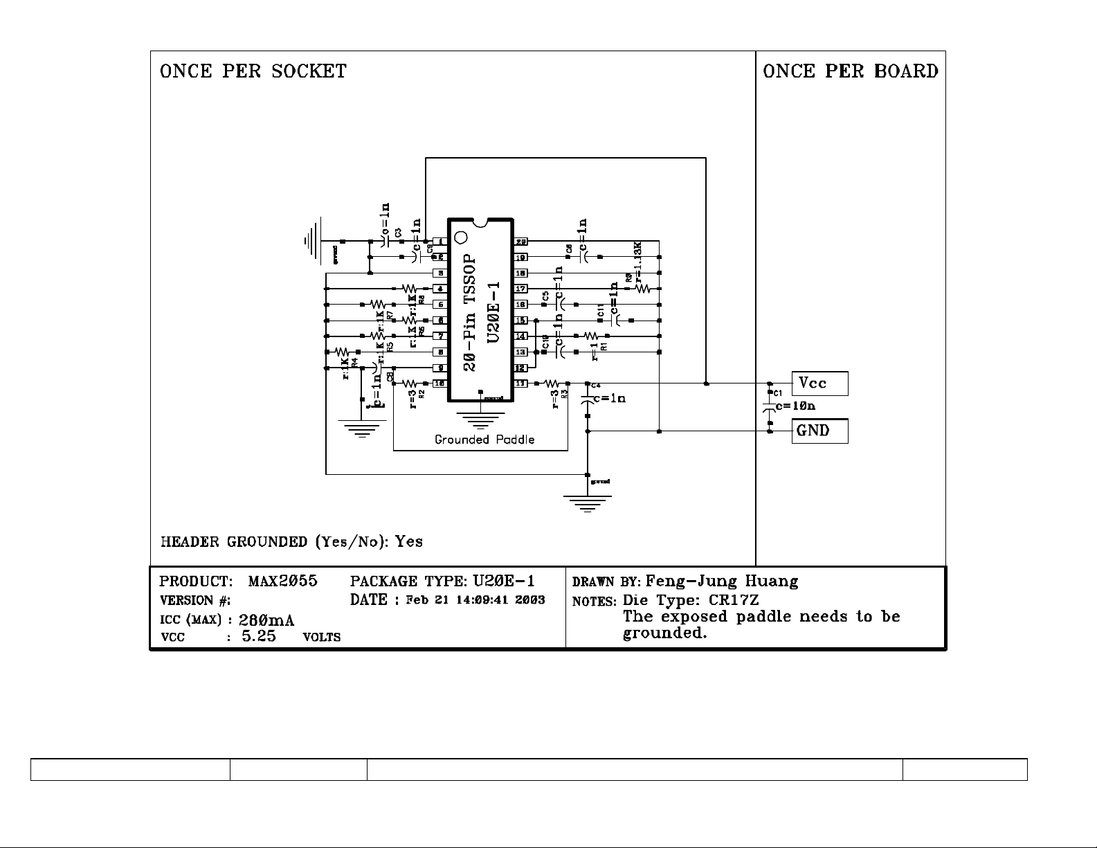
DOCUMENT I.D. 06-7097 REVISION B B
MAXIM TITLE: BI Circuit (MAX2055) CR17Z PAGE 2
 Loading...