

Page 1
现货库存、技术资料、百科信息、热点资讯,精彩尽在鼎好!
General Description
The MAX2045/MAX2046/MAX2047 low-cost, fully integrated vector multipliers alter the magnitude and phase
of an RF signal. Each device is optimized for the UMTS
(MAX2045), DCS/PCS (MAX2046), or cellular/GSM
(MAX2047) frequency bands. These devices feature
differential RF inputs and outputs.
The MAX2045/MAX2046/MAX2047 provide vector
adjustment through the differential I/Q amplifiers. The
I/Q amplifiers can interface with voltage and/or current
digital-to-analog converters (DACs). The voltage inputs
are designed to interface to a voltage-mode DAC, while
the current inputs are designed to interface to a currentmode DAC. An internal 2.5V reference voltage is provided for applications using single-ended voltage DACs.
The MAX2045/MAX2046/MAX2047 operate from a 4.75V
to 5.25V single supply. All devices are offered in a compact 5mm ✕ 5mm, 32-lead thin QFN exposed-paddle
packages.
The MAX2045/MAX2046/MAX2047 evaluation kits are
available, contact factory for availability.
Applications
UMTS/PCS/DCS/Cellular/GSM Base Station
Feed-Forward and Predistortion Power Amplifiers
RF Magnitude and Phase Adjustment
RF Cancellation Loops
Beam-Forming Applications
Features
♦ Multiple RF Frequency Bands of Operation
2040MHz to 2240MHz (MAX2045)
1740MHz to 2060MHz (MAX2046)
790MHz to 1005MHz (MAX2047)
♦ ±0.2dB Gain Flatness
♦ ±1° Phase Flatness
♦ 3dB Control Bandwidth: 260MHz
♦ 15dBm Input IP3
♦ 15dB Gain Control Range
♦ Continuous 360° Phase Control Range
♦ 6.5dB Maximum Gain for Continuous Phase
♦ On-Chip Reference for Single-Ended
Voltage-Mode Operation
♦ 800mW Power Consumption
♦ Space-Saving 5mm x 5mm Thin QFN Package
♦ Single 5V supply
MAX2045/MAX2046/MAX2047
High-Gain Vector Multipliers
________________________________________________________________ Maxim Integrated Products 1
Ordering Information
19-2728; Rev 0; 1/03
For pricing, delivery, and ordering information, please contact Maxim/Dallas Direct! at
1-888-629-4642, or visit Maxim’s website at www.maxim-ic.com.
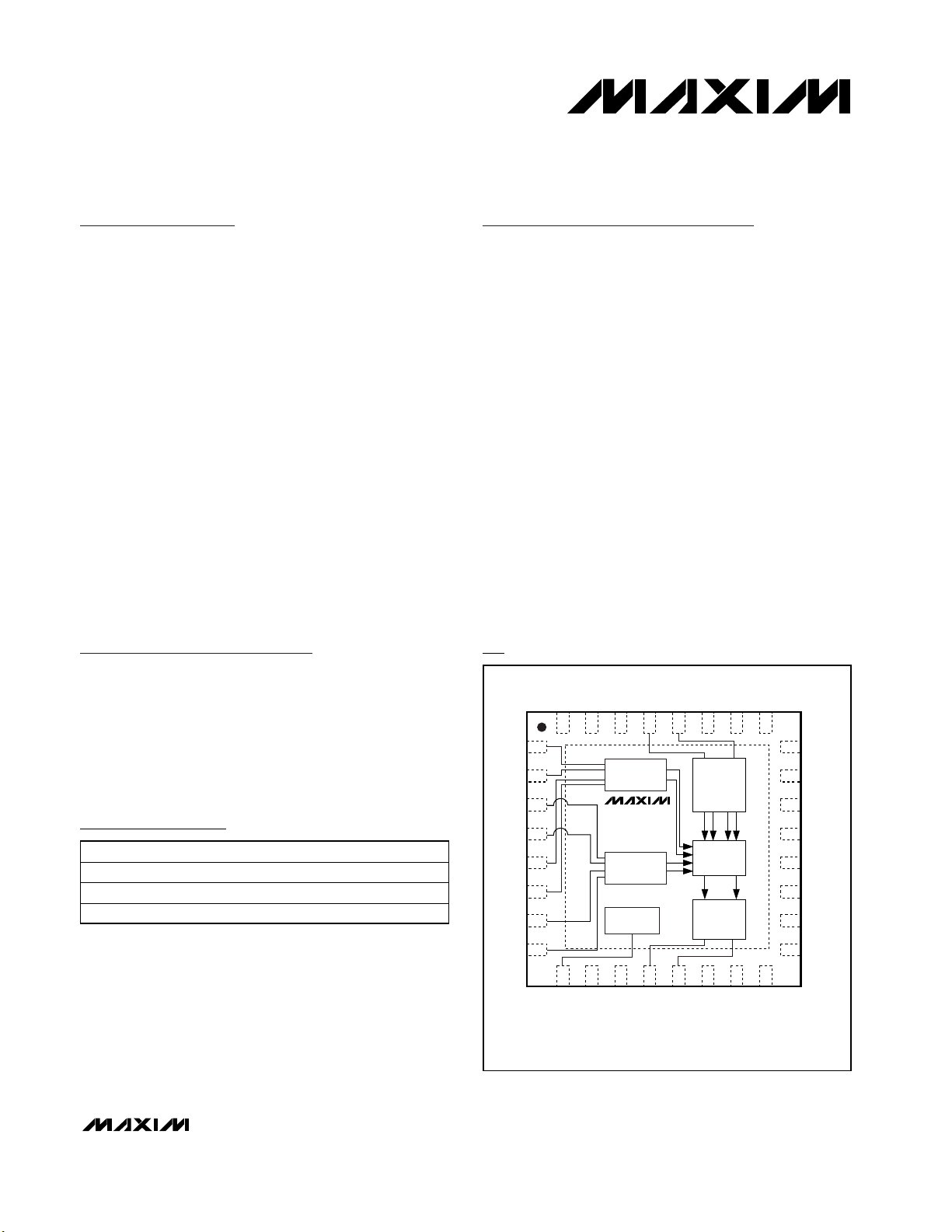
Pin Configuration/Block Diagram
*EP = Exposed paddle.
PART TEMP RANGE PIN-PACKAGE
MAX2045ETJ-T -40°C to +85°C 32 Thin QFN-EP*
MAX2046ETJ-T -40°C to +85°C 32 Thin QFN-EP*
MAX2047ETJ-T -40°C to +85°C 32 Thin QFN-EP*
GND
GND
RFIN1
28
13
GND
27
90°
PHASE
SHIFTER
VECTOR
MULTIPLIER
OUTPUT
STAGE
14
26
25
GND
24
GND
23
RBIAS
22
GND
21
GND
20
GND
19
V
18
V
17
15
16
VQ1
VQ2
GND
313230
VI1
1
VI2
2
3
4
II1
5
6
II2
7
IQ1
8
IQ2
10911
CONTROL
AMPLIFIER I
MAX2045
MAX2046
MAX2047
CONTROL
AMPLIFIER Q
2.5V
REFERENCE
RFIN2
29
12
GND
GND
CC
CC
GND
REFOUT
GND
RFOUT1
QFN
RFOUT2
GND
GND
GND
Page 2
MAX2045/MAX2046/MAX2047
High-Gain Vector Multipliers
2 _______________________________________________________________________________________
ABSOLUTE MAXIMUM RATINGS
DC ELECTRICAL CHARACTERISTICS
(Typical Operating Circuit as shown in Figure 1; VCC= 4.75V to 5.25V, TA= -40°C to +85°C, R
BIAS
= 280Ω, no RF inputs applied, RF
input and output ports are terminated with 50Ω. Typical values are at V
CC
= 5V and TA= +25°C, unless otherwise noted.)
Stresses beyond those listed under “Absolute Maximum Ratings” may cause permanent damage to the device. These are stress ratings only, and functional
operation of the device at these or any other conditions beyond those indicated in the operational sections of the specifications is not implied. Exposure to
absolute maximum rating conditions for extended periods may affect device reliability.
VCCto GND .............................................................-0.3V to +6V
VI1, V12, VQ1, VQ2, RFIN1, RFIN2,
RFOUT1, RFOUT2 ....................................-0.3V to VCC+ 0.3V
RFOUT1, RFOUT2 Sink Current..........................................35mA
REFOUT Source Current.......................................................4mA
II1, II2, IQ1, IQ2 ........................................................-0.3V to +1V
II1, II2, IQ1, IQ2 Sink Current ...........................................+10mA
Continuous RF Input Power (CW)...................................+15dBm
Continuous Power Dissipation (TA= +70°C)
32-Pin Thin QFN (derate 21.3mW/°C above +70°C) .......1.7W
Operating Temperature Range ...........................-40°C to +85°C
Junction Temperature......................................................+150°C
Storage Temperature Range .............................-40°C to +150°C
Lead Temperature (soldering, 10s) .................................+300°C
AC ELECTRICAL CHARACTERISTICS
(Typical Operating Circuit as shown in Figure 1; VCC= 4.75V to 5.25V, TA= -40°C to +85°C, R
BIAS
= 280Ω, fIN= 2.14GHz
(MAX2045), f
IN
= 1.9GHz (MAX2046), fIN= 915MHz (MAX2047), input current range = 0 to 4mA (if using a current-mode DAC), and
differential input voltage range = 0 to 0.707V (if using a voltage-mode DAC). If using a current-mode DAC, voltage mode I/Q inputs
are left open. If using a voltage-mode DAC, all current-mode I/Q inputs are left open. Typical values are at V
CC
= 5V and TA=
+25°C, unless otherwise noted.) (Notes 1, 2, 3)
Supply Voltage Range V
Differential Input Resistance,
VI1 to VI2, VQ1 to VQ2
Common-Mode Input Voltage,
VI1, VI2, VQ1, VQ2
Input Resistance, II1, II2, IQ1,
IQ2
Reference Voltage V
PARAMETER SYMBOL CONDITIONS MIN TYP MAX UNITS
CC
MAX2045 120 160 200
CC
V
CM
REFOUT
MAX2046 120 160 200Operating Supply Current I
MAX2047 120 160 200
Input resistance between VI1 and VI2 or
VQ1 and VQ2
Single-ended resistance to ground 150 200 250 Ω
REFOUT unloaded 2.3 2.45 2.6 V
4.75 5 5.25 V
6.5 9 11.5 kΩ
2.5 V
mA
RF Differential Input Impedance 50 Ω
RF Differential Output Impedance 300 Ω
RF Differential Load Impedance 200 Ω
Continuous Phase Range 0 360 Degrees
PARAMETER CONDITIONS MIN TYP MAX UNITS
Page 3
MAX2045/MAX2046/MAX2047
High-Gain Vector Multipliers
_______________________________________________________________________________________ 3
MAX2045 ELECTRICAL CHARACTERISTICS
(Typical Operating Circuit as shown in Figure 1; VCC= 4.75V to 5.25V, TA= -40°C to +85°C, R
BIAS
= 280Ω, fIN= 2.14GHz, input current range = 0 to 4mA (if using a current-mode DAC), and differential input voltage range = 0 to 0.707V (if using a voltage-mode
DAC). If using a current-mode DAC, voltage mode I/Q inputs are left open. If using a voltage-mode DAC, all current-mode I/Q inputs
are left open. Typical values are at V
CC
= 5V and TA= +25°C, unless otherwise noted.) (Notes 1, 2, 3)
Frequency Range 2040 2240 MHz
RF Input Return Loss -14 dB
RF Output Return Loss -16.4 dB
VOLTAGE MODE
Power Gain
Power-Gain Range
Reverse Isolation Over entire control range -74 dB
Maximum Power Gain for
Continuous Coverage of Phase
Change
Maximum Power Gain with
Reduced Phase Coverage
Group Delay VI = VQ = 0.707V (radius = 1V) 1.38 ns
Gain Drift Over Temperature VI = VQ = 0.707V (radius = 1V) -0.027 dB/°C
Gain Flatness Over Frequency
Phase Flatness Over Frequency
Output Noise Power
IP1dB
IIP3
PARAMETER CONDITIONS MIN TYP MAX UNITS
VI = VQ = 0.707V (radius = 1V) 7
VI = VQ = 0.5V (radius = 0.707V) 3.4
VI = VQ = 0.25V (radius = 0.35V) -3
VI = VQ = 0.125V
Difference in gain between VI = VQ = 0.707V and
VI = VQ = 0.125V
0 to 360° (radius = 1V) 6.1 dB
0 to 360° (radius = 1V) 7 dB
VI = VQ = 0.707V (radius = 1V); UMTS,
= 2140MHz ±100MHz
f
IN
Electrical delay removed, VI = VQ = 0.707V
(radius = 1V), UMTS, f
VI = VQ = 0.707V (radius = 1V) -147.7
VI = VQ = 0.5V (radius = 0.707V) -148.3
VI = VQ = 0.25V (radius = 0.35V) -148.2
VI = VQ = 0.125V
VI = VQ = 0.707V (radius = 1V) 6.7
VI = VQ = 0.125V
VI = VQ = 0.707V (radius = 1V) 15.2
VI = VQ = 0.125V
(radius = 0.175V) -8.7
= 2140MHz ±100MHz
IN
(radius = 0.175V) -148.1
(radius = 0.175V) 9.3
(radius = 0.175V) 14.7
15.7 dB
±0.21 dB
±0.2 Degrees
dB
dBm/Hz
dBm
dBm
Page 4
MAX2045/MAX2046/MAX2047
High-Gain Vector Multipliers
4 _______________________________________________________________________________________
MAX2046 ELECTRICAL CHARACTERISTICS
(Typical Operating Circuit as shown in Figure 1; VCC= 4.75V to 5.25V, TA= -40°C to +85°C, R
BIAS
= 280Ω, fIN= 1.9GHz, input current range = 0 to 4mA (if using a current-mode DAC), and differential input voltage range = 0 to 0.707V (if using a voltage-mode
DAC). If using a current-mode DAC, voltage mode I/Q inputs are left open. If using a voltage-mode DAC, all current-mode I/Q inputs
are left open. Typical values are at V
CC
= 5V and TA= +25°C, unless otherwise noted.) (Notes 1, 2, 3)
MAX2045 ELECTRICAL CHARACTERISTICS (continued)
(Typical Operating Circuit as shown in Figure 1; VCC= 4.75V to 5.25V, TA= -40°C to +85°C, R
BIAS
= 280Ω, fIN= 2.14GHz, input current range = 0 to 4mA (if using a current-mode DAC), and differential input voltage range = 0 to 0.707V (if using a voltage-mode
DAC). If using a current-mode DAC, voltage mode I/Q inputs are left open. If using a voltage-mode DAC, all current-mode I/Q inputs
are left open. Typical values are at V
CC
= 5V and TA= +25°C, unless otherwise noted.) (Notes 1, 2, 3)
CURRENT MODE
Power Gain (Note 4)
Power-Gain Range
Gain Flatness Over Frequency
Phase Flatness Over Frequency
PARAMETER CONDITIONS MIN TYP MAX UNITS
II1 = IQ1 = 4mA, II2 = IQ2 = 0mA 6.2
II1 = IQ1 = 1mA, II2 = IQ2 = 0mA -8.7
Difference in gain between II1 = IQ1 = 4mA, II2 = IQ2 =
0mA and II1 = IQ1 = 1mA, II2 = IQ2 = 0mA
II1 = IQ1 = 4mA, II2 = IQ2 = 0mA; UMTS,
f
= 2140MHz ±100MHz
IN
Electrical delay removed, II1 = IQ1 = 4mA,
II2 = IQ2 = 0mA
Frequency Range 1740 2060 MHz
RF Input Return Loss -21.1 dB
RF Output Return Loss -21.7 dB
VOLTAGE MODE
Power Gain
Power-Gain Range
Reverse Isolation Over entire control range -76 dB
Maximum Power Gain for
Continuous Coverage of Phase
Change
Maximum Power Gain with
Reduced Phase Coverage
Group Delay VI = VQ = 0.707V (radius = 1V) 1.54 ns
Gain Drift Over Temperature VI = VQ = 0.707V (radius = 1V) -0.026 dB/°C
Gain Flatness Over Frequency
PARAMETER CONDITIONS MIN TYP MAX UNITS
VI = VQ = 0.707V (radius = 1V) 7.4
VI = VQ = 0.5V (radius = 0.707V) 3.8
VI = VQ = 0.25V
VI = VQ = 0.125V
Difference in gain between VI = VQ = 0.707V and
VI = VQ = 0.125V
0 to 360° (radius = 1V) 6.5 dB
0 to 360° (radius = 1V) 7.4 dB
VI = VQ = 0.707V
(radius = 1V)
(radius = 0.35V) -2.5
(radius = 0.175V) -8.2
PCS, fIN = 1960MHz
±100MHz
DCS, f
±100MHz
= 1842.5MHz
IN
14.9 dB
±0.27 dB
±0.8 Degrees
15.6 dB
±0.14
±0.3
dB
dB
dB
Page 5
MAX2045/MAX2046/MAX2047
High-Gain Vector Multipliers
_______________________________________________________________________________________ 5
MAX2046 ELECTRICAL CHARACTERISTICS (continued)
(Typical Operating Circuit as shown in Figure 1; VCC= 4.75V to 5.25V, TA= -40°C to +85°C, R
BIAS
= 280Ω, fIN= 1.9GHz, input current range = 0 to 4mA (if using a current-mode DAC), and differential input voltage range = 0 to 0.707V (if using a voltage-mode
DAC). If using a current-mode DAC, voltage mode I/Q inputs are left open. If using a voltage-mode DAC, all current-mode I/Q inputs
are left open. Typical values are at V
CC
= 5V and TA= +25°C, unless otherwise noted.) (Notes 1, 2, 3)
Phase Flatness Over Frequency
Output Noise Power
IP1dB
IIP3
CURRENT MODE
Power Gain (Note 4)
Power-Gain Range
Gain Flatness Over Frequency
Phase Flatness Over Frequency
PARAMETER CONDITIONS MIN TYP MAX UNITS
PCS, fIN = 1960MHz
Electrical delay removed,
VI = VQ = 0.707V
VI = VQ = 0.707V (radius = 1V) -146.8
VI = VQ = 0.5V (radius = 0.707V) -147.4
VI = VQ = 0.25V (radius = 0.35V) -147.4
VI = VQ = 0.125V
VI = VQ = 0.707V (radius = 1V) 6.5
VI = VQ = 0.125V
VI = VQ = 0.707V (radius = 1V) 15.2
VI = VQ = 0.125V
II1 = IQ1 = 4mA, II2 = IQ2 = 0mA 6.6
II1 = IQ1 = 1mA, II2 = IQ2 = 0mA -8.2
Difference in gain between II1 = IQ1 = 4mA, II2 = IQ2 =
0mA and II1 = IQ1 = 1mA, II2 = IQ2 = 0mA
II1 = IQ1 = 4mA, II2 = IQ2 =
0mA
Electrical delay removed,
II1 = IQ1 = 4mA,
II2 = IQ2 = 0mA
(radius = 1V)
(radius = 0.175V) -147.3
(radius = 0.175V) 9.1
(radius = 0.175V) 14.8
±100MHz
DCS, f
±100MHz
PCS, fIN = 1960MHz
±100MHz
DCS, f
±100MHz
PCS, fIN = 1960MHz
±100MHz
DCS, f
±100MHz
= 1842.5MHz
IN
= 1842.5MHz
IN
= 1842.5MHz
IN
±1.3
±1.2
14.8 dB
±0.14
±0.33
±0.8
±1.6
Degrees
dBm/Hz
dBm
dBm
dB
dB
Degrees
Page 6
MAX2045/MAX2046/MAX2047
High-Gain Vector Multipliers
6 _______________________________________________________________________________________
MAX2047 ELECTRICAL CHARACTERISTICS
(Typical Operating Circuit as shown in Figure 1; VCC= 4.75V to 5.25V, TA= -40°C to +85°C, R
BIAS
= 280Ω, fIN= 915MHz, input current range = 0 to 4mA (if using a current-mode DAC), and differential input voltage range = 0 to 0.707V (if using a voltage-mode
DAC). If using a current-mode DAC, voltage mode I/Q inputs are left open. If using a voltage-mode DAC, all current-mode I/Q inputs
are left open. Typical values are at V
CC
= 5V and TA= +25°C, unless otherwise noted.) (Notes 1, 2, 3)
Frequency Range 790 1005 MHz
RF Input Return Loss -21.8 dB
RF Output Return Loss -11.7 dB
VOLTAGE MODE
Power Gain
Power-Gain Range
Reverse Isolation Over entire control range -75 dB
Maximum Power Gain for
Continuous Coverage of Phase
Change
Maximum Power Gain with
Reduced Phase Coverage
Group Delay VI = VQ = 0.707V (radius = 1V) 2.02 ns
Gain Drift Over Temperature VI = VQ = 0.707V (radius = 1V) -0.024 dB/°C
PARAMETER CONDITIONS MIN TYP MAX UNITS
Gain Flatness Over Frequency
Phase Flatness Over Frequency
VI = VQ = 0.707V (radius = 1V) 8.4
VI = VQ = 0.5V
VI = VQ = 0.25V
VI = VQ = 0.125V
Difference in gain between VI = VQ = 0.707V and
VI = VQ = 0.125V
0 to 360° (radius = 1V) 7.1 dB
0 to 360° (radius = 1V) 8.4 dB
VI = VQ = 0.707V
(radius = 1V)
E l ectr i cal d el ay r em oved ,
V I = VQ = 0.707V
= 1V)
(radius = 0.707V) 5.1
(radius = 0.35V) -0.9
(radius = 0.175V) -6.3
GSM, fIN = 942.5MHz
±62.5MHz
US cell, fIN = 881.5MHz
±62.5MHz
JCDMA, fIN = 850MHz
±60MHz
(radius
KDI/JDC/PDC, f
±30MHz
GSM, fIN = 942.5MHz
±62.5MHz
US cell, fIN = 881.5MHz
±62.5MHz
JCDMA, fIN = 850MHz
±60MHz
KDI/JDC/PDC, f
±30MHz
= 820MHz
IN
= 820MHz
IN
14.7 dB
±0.25
±0.13
±0.1
±0.1
±0.9
±1.1
±1.2
±0.3
dB
dB
Degrees
Page 7
MAX2045/MAX2046/MAX2047
High-Gain Vector Multipliers
_______________________________________________________________________________________ 7
Note 1: Guaranteed by design and characterization.
Note 2: All specifications reflect losses and delays of external components (matching components, baluns, and PC board traces).
Output measurements taken at the RF OUTPUT of the Typical Operating Circuit.
Note 3: Radius is defined as (VI
2
+ VQ2)
0.5
. VI denotes the difference between VI1 and VI2. VQ denotes the difference between VQ1
and VQ2. For differential operation: VI1 = V
REF
+ 0.5 ✕ VI, VI2 = V
REF
- 0.5 ✕ VI, VQ1 = V
REF
+ 0.5 ✕ VQ, VQ2 = V
REF
- 0.5 ✕
VQ. For single-ended operation: VI1 = V
REF
+ VI, VI2 = V
REF
, VQ1 = V
REF
+ VQ, VQ2 = V
REF
.
Note 4: When using the I/Q current inputs, maximum gain occurs when one differential input current is zero and the other corre-
sponding differential input is 5mA. Minimum gain occurs when both differential inputs are equal.
MAX2047 ELECTRICAL CHARACTERISTICS (continued)
(Typical Operating Circuit as shown in Figure 1; VCC= 4.75V to 5.25V, TA= -40°C to +85°C, R
BIAS
= 280Ω, fIN= 915MHz, input current range = 0 to 4mA (if using a current-mode DAC), and differential input voltage range = 0 to 0.707V (if using a voltage-mode
DAC). If using a current-mode DAC, voltage mode I/Q inputs are left open. If using a voltage-mode DAC, all current-mode I/Q inputs
are left open. Typical values are at V
CC
= 5V and TA= +25°C, unless otherwise noted.) (Notes 1, 2, 3)
PARAMETER CONDITIONS MIN TYP MAX UNITS
VI = VQ = 0.707V (radius = 1V) -147.5
Output Noise Power
IP1dB
IIP3
VI = VQ = 0.5V (radius = 0.707V) -148.4
VI = VQ = 0.25V (radius = 0.35V) -148.6
VI = VQ = 0.125V
(radius = 0.175V) -148.6
VI = VQ = 0.707V (radius = 1V) 6.1
VI = VQ = 0.125V
(radius = 0.175V) 6.9
VI = VQ = 0.707V (radius = 1V) 15.6
VI = VQ = 0.125V
(radius = 0.175V) 14.1
CURRENT MODE
Power Gain (Note 4)
Power-Gain Range
II1 = IQ1 = 4mA, II2 = IQ2 = 0mA 8.1
II1 = IQ1 = 1mA, II2 = IQ2 = 0mA -6.2
Difference in gain between II1 = IQ1 = 4mA, II2 = IQ2 =
0mA and II1 = IQ1 = 1mA, II2 = IQ2 = 0mA
GSM, fIN = 942.5MHz
±62.5MHz
US cell, fIN = 881.5MHz
Gain Flatness Over Frequency
II1 = IQ1 = 4mA,
II2 = IQ2 = 0mA
±62.5MHz
JCDMA, fIN = 850MHz
±60MHz
KDI/JDC/PDC, f
= 820MHz
IN
±30MHz
GSM, fIN = 942.5MHz
±62.5MHz
US cell, fIN = 881.5MHz
±62.5MHz
JCDMA, fIN = 850MHz
Phase Flatness Over Frequency
Electrical delay removed,
II1 = IQ1 = 4mA,
II2 = IQ2 = 0mA
±60MHz
KDI/JDC/PDC, f
= 820MHz
IN
±30MHz
14.3 dB
±0.25
±0.12
±0.1
±0.1
±0.8
±1.1
±1.3
±0.4
dBm/Hz
dBm
dBm
dB
dB
Degrees
Page 8

MAX2045/MAX2046/MAX2047
High-Gain Vector Multipliers
8 _______________________________________________________________________________________
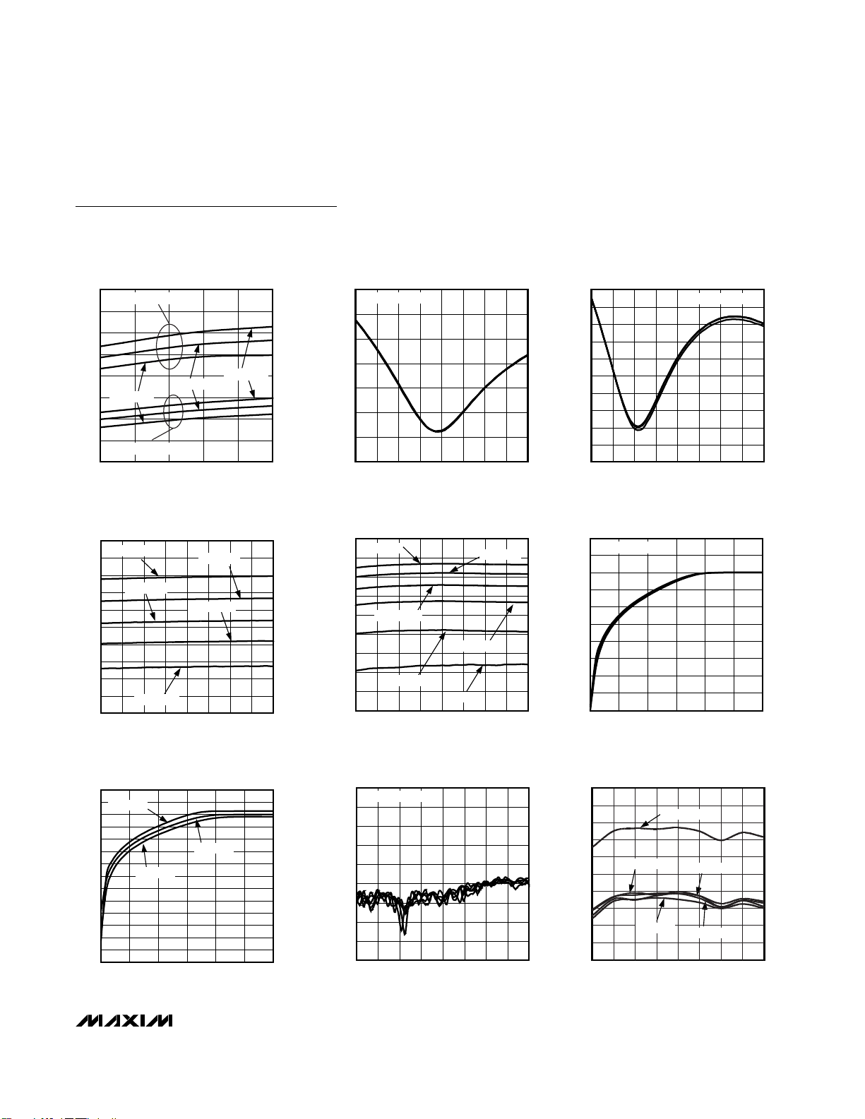
Typical Operating Characteristics (MAX2045)
(VCC= 5V, fIN= 2140MHz, V_1 = VI1 and VQ1, V_2 = VI2 and VQ2, I_1 = II1 and IQ1, I_2 = II2 and IQ2, VI1 = VQ1 = 3.2V, VI2 =
VQ2 = REFOUT, P
IN
= -15dBm per tone at 1MHz offset (IIP3), and TA= +25°C, unless otherwise noted.)
REFOUT AND SUPPLY CURRENT
vs. TEMPERATURE AND SUPPLY VOLTAGE
MAX2045 toc01
TEMPERATURE (°C)
SUPPLY CURRENT (mA)
603510-15
150
160
170
180
190
200
210
220
230
140
REFOUT (V)
2.46
2.45
2.44
2.47
2.48
2.49
2.50
2.51
2.52
2.43
-40 85
REFOUT LOADED WITH V_2
VCC = 4.75V
VCC = 5.0V
VCC = 5.25V
SUPPLY CURRENT
INPUT RETURN LOSS vs. FREQUENCY
MAX2045 toc02
FREQUENCY (MHz)
INPUT RETURN LOSS (dB)
22502200215021002050
19
18
17
16
15
14
13
12
11
10
20
2000 2300
V_1 = 2.55V TO 3.5V
OUTPUT RETURN LOSS vs. FREQUENCY
MAX2045 toc03
FREQUENCY (MHz)
OUTPUT RETURN LOSS (dB)
22502200215021002050
19
18
17
16
15
14
13
12
20
21
22
2000 2300
V_1 = 2.55V TO 3.5V
GAIN vs. FREQUENCY
MAX2045 toc04
FREQUENCY (MHz)
GAIN (dB)
22502200215021002050
-15
-10
-5
0
5
10
15
20
-20
-25
-30
2000 2300
V_1 = 3.5V
V_1 = 3.0V
V_1 = 2.75V
V_1 = 2.625V
V_1 = 2.55V
GAIN vs. FREQUENCY
MAX2045 toc05
FREQUENCY (MHz)
GAIN (dB)
22502200215021002050
-15
-10
-5
0
5
10
15
-20
-25
-30
2000 2300
I_1 = 3mA
I_1 = 2mA
I_1 = 4mA
I_1 = 5mA
I_1 = 0
I_1 = 1mA
GAIN vs. CONTROL VOLTAGE (VI1 = VQ1)
MAX2045 toc06
CONTROL VOLTAGE VI1, VQ1 (V)
GAIN (dB)
3.753.503.253.002.75
-25
-20
-15
-10
-5
0
5
10
15
-30
2.50 4.00
VCC = 4.75V TO 5.25V
GAIN vs. CONTROL VOLTAGE (VI1 = VQ1)
MAX2045 toc07
CONTROL VOLTAGE VI1, VQ1 (V)
GAIN (dB)
3.753.503.253.002.75
-45
-40
-35
-30
-25
-20
-15
-10
-5
0
5
10
15
20
-50
2.50 4.00
TA = +85°C
TA = +25°C
TA = -40°C
REVERSE ISOLATION vs. FREQUENCY
MAX2045 toc08
FREQUENCY (MHz)
ISOLATION (dB)
22502200215021002050
110
100
90
80
70
60
50
40
30
120
2000 2300
V_1 = 2.55V TO 3.5V
OUTPUT NOISE POWER vs. FREQUENCY
MAX2045 toc09
FREQUENCY (MHz)
OUTPUT NOISE POWER (dBm/Hz)
22502200215021002050
-148.5
-148.0
-147.5
-147.0
-146.5
-146.0
-145.5
-145.0
-144.5
-144.0
-149.0
2000 2300
V_1 = 2.625V
V_1 = 3.5V
V_1 = 2.55V
V_1 = 3V
V_1 = 2.75V
Page 9

MAX2045/MAX2046/MAX2047
High-Gain Vector Multipliers
_______________________________________________________________________________________ 9
Typical Operating Characteristics (MAX2045) (continued)
(VCC= 5V, fIN= 2140MHz, V_1 = VI1 and VQ1, V_2 = VI2 and VQ2, I_1 = II1 and IQ1, I_2 = II2 and IQ2, VI1 = VQ1 = 3.2V, VI2 =
VQ2 = REFOUT, PIN= -15dBm per tone at 1MHz offset (IIP3), and TA= +25°C, unless otherwise noted.)
OUTPUT NOISE POWER
vs. CONTROL VOLTAGE (VI1 = VQ1)
-144.0
-144.5
-145.0
-145.5
-146.0
-146.5
-147.0
-147.5
OUTPUT NOISE POWER (dBm/Hz)
-148.0
-148.5
-149.0
2.50 4.00
TA = +85°C
TA = +-40°C
TA = +25°C
CONTROL VOLTAGE VI1, VQ1 (V)
3.753.503.253.002.75
-144.0
-144.5
MAX2045 toc10
-145.0
-145.5
-146.0
-146.5
-147.0
-147.5
OUTPUT NOISE POWER (dBm/Hz)
-148.0
-148.5
-149.0
2.50 4.00
INPUT P1-dB COMPRESSION
vs. FREQUENCY
9.0
V_1 = 3.2V
8.5
8.0
7.5
TA = +25°C
7.0
6.5
INPUT P1-dB (dBm)
6.0
5.5
5.0
2000 2300
FREQUENCY (MHz)
TA = +85°C
TA = -40°C
MAX2045 toc13
225022002050 2100 2150
16
15
14
13
12
11
10
9
INPUT P1-dB (dBm)
8
7
6
5
2.50 4.00
OUTPUT NOISE POWER
vs. CONTROL VOLTAGE (VI1 = VQ1)
VCC = 5.25V
VCC = 5.0V
VCC = 4.75V
3.753.503.253.002.75
CONTROL VOLTAGE VI1, VQ1 (V)
INPUT P1-dB COMPRESSION
vs. CONTROL VOLTAGE (VI1 = VQ1)
VCC = 5.25V
VCC = 5.0V
VCC = 4.75V
3.753.503.253.002.75
CONTROL VOLTAGE VI1, VQ1 (V)
9.0
8.5
MAX2045 toc11
8.0
7.5
7.0
6.5
INPUT P1-dB (dBm)
6.0
5.5
5.0
MAX2045 toc14
INPUT P1-dB (dBm)
INPUT P1-dB COMPRESSION
vs. FREQUENCY
V_1 = 3.2V
VCC = 5.25V
VCC = 5.0V
VCC = 4.75V
2000 2300
FREQUENCY (MHz)
225022002050 2100 2150
INPUT P1-dB COMPRESSION
vs. CONTROL VOLTAGE (VI1 = VQ1)
16
15
14
13
12
11
10
9
8
7
6
5
2.50 4.00
TA = +85°C
TA = +25°C
TA = -40°C
3.753.503.253.002.75
CONTROL VOLTAGE VI1, VQ1 (V)
MAX2045 toc12
MAX2045 toc15
16.0
V_1 = 3.2V
15.5
15.0
14.5
IIP3 (dBm)
14.0
13.5
13.0
2000 2300
VCC = 5.25V
VCC = 5.0V
VCC = 4.75V
FREQUENCY (MHz)
IIP3 vs. FREQUENCY
16.0
IIP3 vs. FREQUENCY
V_1 = 3.2V
15.5
MAX2045 toc16
15.0
14.5
IIP3 (dBm)
14.0
13.5
22502200215021002050
13.0
2000 2300
TA = +85°C
TA = -40°C
FREQUENCY (MHz)
MAX2045 toc17
TA = +25°C
22502200215021002050
IIP3 vs. CONTROL VOLTAGE (VI1 = VQ1)
19
18
17
16
15
14
13
VCC = 4.75V
12
IIP3 (dBm)
11
10
9
8
7
6
5
2.50 4.00
CONTROL VOLTAGE VI1 , VQ1, (V)
VCC = 5.25V
VCC = 5.0V
MAX2045 toc18
3.753.503.253.002.75
Page 10

MAX2045/MAX2046/MAX2047
High-Gain Vector Multipliers
10 ______________________________________________________________________________________
Typical Operating Characteristics (MAX2045) (continued)
(VCC= 5V, fIN= 2140MHz, V_1 = VI1 and VQ1, V_2 = VI2 and VQ2, I_1 = II1 and IQ1, I_2 = II2 and IQ2, VI1 = VQ1 = 3.2V, VI2 =
VQ2 = REFOUT, P
IN
= -15dBm per tone at 1MHz offset (IIP3), and TA= +25°C, unless otherwise noted.)
IIP3 vs. CONTROL VOLTAGE (VI1 = VQ1)
19
18
17
16
15
14
13
12
IIP3 (dBm)
11
10
9
8
7
6
5
2.50 4.00
GAIN vs. PHASE
TA = +85°C
TA = -40°C
CONTROL VOLTAGE VI1 , VQ1, (V)
TA = +25°C
10
RADIUS = 1
8
MAX2045 toc19
3.753.503.253.002.75
6
4
2
0
-2
RADIUS = 0.75
-4
GAIN (dB)
RADIUS = 0.5
-6
-8
-10
-12
RADIUS = 0.25
-14
-16
0 360
RADIUS = 0.875
RADIUS = 0.625
RADIUS = 0.375
RADIUS = 0.125
315270180 22590 13545
PHASE (DEGREES)
MAX2045 toc20
86.0
S21 PHASE vs. FREQUENCY
V_1 = 3.2V
85.5
ONE ELECTRICAL DELAY
85.0
REMOVED AT 5V
84.5
84.0
83.5
83.0
82.5
PHASE (DEGREES)
82.0
81.5
81.0
80.5
80.0
2000 2300
VCC = 5.V
FREQUENCY (MHz)
VCC = 5.25V
VCC = 4.75V
22502200215021002050
MAX2045 toc21
80.0
V_1 = 2.65V
79.5
ONE ELECTRICAL DELAY
79.0
REMOVED AT 5V
78.5
78.0
77.5
77.0
76.5
PHASE (DEGREES)
76.0
75.5
75.0
74.5
74.0
2000 2300
VCC = 5V
FREQUENCY (MHz)
VCC = 5.25V
VCC = 4.75V
22502200215021002050
MAX2045 toc22
100
95
90
85
80
PHASE (DEGREES)
75
70
65
S21 PHASE vs. FREQUENCY
S21 PHASE vs. FREQUENCY
V_1 = 3.2V
ONE ELECTRICAL DELAY
REMOVED AT +25°C
TA = +25°C
TA = +85°C
2000 2300
FREQUENCY (MHz)
TA = -40°C
GROUP DELAY vs. FREQUENCY
1.90
V_1 = 2.55V TO 3.5V
1.85
1.80
1.75
1.70
1.65
1.60
1.55
1.50
1.45
1.40
1.35
GROUP DELAY (ns)
1.30
1.25
1.20
1.15
1.10
1.05
1.00
2000 2300
FREQUENCY (MHz)
22502200215021002050
MAX2045 toc25
DIFFERENTIAL CONTROL
SIGNAL
GAIN
90
V_1 = 2.65V
ONE ELECTRICAL DELAY
85
MAX2045 toc23
22502200215021002050
REMOVED AT +25°C
80
75
PHASE (DEGREES)
70
65
60
2000 2300
SWITCHING SPEED
SEE SWITCHING SPEED SECTION IN THE
APPLICATIONS INFORMATION
-0.7V
MAX GAIN, Q3
SWITCHING SPEED (1ns/div)
+0.7V
MIN GAIN,
ORIGIN
MAX GAIN, Q1
S21 PHASE vs. FREQUENCY
TA = -40°C
MAX2045 toc24
TA = +25°C
TA = +85°C
22502200215021002050
FREQUENCY (MHz)
MAX2045 toc26
Page 11
MAX2045/MAX2046/MAX2047
High-Gain Vector Multipliers
______________________________________________________________________________________ 11
Typical Operating Characteristics (MAX2046)
(VCC= 5V, fIN= 1900MHz, V_1 = VI1 and VQ1, V_2 = VI2 and VQ2, I_1 = II1 and IQ1, I_2 = II2 and IQ2, VI1 = VQ1 = 3.2V, VI2 =
VQ2 = REFOUT, PIN= -15dBm per tone at 1MHz offset (IIP3), and TA= +25°C, unless otherwise noted.)
REFOUT AND SUPPLY CURRENT
vs. TEMPERATURE AND SUPPLY VOLTAGE
220
REFOUT LOADED WITH V_2
210
200
190
180
VCC = 4.75V
170
SUPPLY CURRENT (mA)
160
150
SUPPLY CURRENT
140
-40 85
VCC = 5.0V
TEMPERATURE (°C)
VCC = 5.25V
GAIN vs. FREQUENCY
20
V_1 = 3.5V
15
10
GAIN (dB)
-10
-15
-20
-25
-30
V_1 = 2.75V
5
0
-5
V_1 = 2.55V
1700 2100
FREQUENCY (MHz)
V_1 = 3.0V
V_1 = 2.625V
MAX2046 toc27
603510-15
2050200019501900185018001750
2.52
2.51
2.50
2.49
2.48
2.47
2.46
2.45
2.44
MAX2046 toc30
REFOUT (V)
INPUT RETURN LOSS vs. FREQUENCY
10
V_1 = 2.55V TO 3.5V
12
14
16
18
20
INPUT RETURN LOSS (dB)
22
24
1700 2100
FREQUENCY (MHz)
2000 205019501850 190018001750
GAIN vs. FREQUENCY
15
I_1 = 5mA
10
5
0
-5
I_1 = 3mA
-10
GAIN (dB)
-15
-20
-25
-30
1700 2100
I_1 = 1mA
FREQUENCY (MHz)
I_1 = 2mA
I_1 = 0
I_1 = 4mA
2050200019501850 190018001750
OUTPUT RETURN LOSS vs. FREQUENCY
12
13
MAX2046 toc28
14
15
16
17
18
19
OUTPUT RETURN LOSS (dB)
20
21
22
1700 2100
GAIN vs. CONTROL VOLTAGE (VI1 = VQ1)
20
VCC = 4.75V TO 5.25V
15
MAX2046 toc31
10
5
0
-5
GAIN (dB)
-10
-15
-20
-25
-30
2.50 4.00
V_1 = 2.55V TO 3.5V
2050200019501850 190018001750
FREQUENCY (MHz)
3.753.503.253.002.75
CONTROL VOLTAGE VI1, VQ1 (V)
MAX2046 toc29
MAX2046 toc32
GAIN vs. CONTROL VOLTAGE (VI1 = VQ1)
20
15
TA = -40°C
10
5
0
-5
-10
-15
GAIN (dB)
-20
-25
-30
-35
-40
-45
-50
2.50 4.00
TA = +85°C
CONTROL VOLTAGE VI1, VQ1 (V)
TA = +25°C
REVERSE ISOLATION vs. FREQUENCY
30
V_1 = 2.55V TO 3.5V
40
MAX2046 toc33
3.753.503.253.002.75
50
60
70
80
ISOLATION (dB)
90
100
110
120
1700 2100
FREQUENCY (MHz)
MAX2046 toc34
2050200019501900185018001750
OUTPUT NOISE POWER vs. FREQUENCY
-144.0
-144.5
-145.0
-145.5
-146.0
-146.5
-147.0
-147.5
OUTPUT NOISE POWER (dBm/Hz)
-148.0
-148.5
-149.0
1700 2100
1750
V_1 = 2.55V
V_1 = 3V
1850
1800
FREQUENCY (MHz)
V_1 = 3.5V
V_1 = 2.625V
V_1 = 2.75V
1900
MAX2046 toc35
205020001950
Page 12

MAX2045/MAX2046/MAX2047
High-Gain Vector Multipliers
12 ______________________________________________________________________________________
0
Typical Operating Characteristics (MAX2046) (continued)
(VCC= 5V, fIN= 1900MHz, V_1 = VI1 and VQ1, V_2 = VI2 and VQ2, I_1 = II1 and IQ1, I_2 = II2 and IQ2, VI1 = VQ1 = 3.2V, VI2 =
VQ2 = REFOUT, P
IN
= -15dBm per tone at 1MHz offset (IIP3), and TA= +25°C, unless otherwise noted.)
OUTPUT NOISE POWER
vs. CONTROL VOLTAGE (VI1 = VQ1)
MAX2046 toc36
CONTROL VOLTAGE VI1, VQ1 (V)
OUTPUT NOISE POWER (dBm/Hz)
3.753.503.253.002.75
-148.5
-148.0
-147.5
-147.0
-146.5
-146.0
-145.5
-145.0
-144.5
-144.0
-149.0
2.50 4.00
TA = -40°C
TA = +85°C
TA = +25°C
9.0
V_1 = 3.2V
8.5
8.0
7.5
7.0
6.5
INPUT P1-dB (dBm)
6.0
5.5
5.0
1700 2100
OUTPUT NOISE POWER
vs. CONTROL VOLTAGE (VI1 = VQ1)
-144.0
VCC = 4.75V
VCC = 5.25V
VCC = 5.0V
3.753.503.253.002.75
CONTROL VOLTAGE VI1, VQ1 (V)
INPUT P1-dB COMPRESSION
VCC = 5.25V
VCC = 5.0V
3.753.503.253.002.75
CONTROL VOLTAGE VI1, VQ1 (V)
INPUT P1-dB COMPRESSION
vs. FREQUENCY
TA = +25°C
FREQUENCY (MHz)
TA = +85°C
TA = -40°C
-144.5
-145.0
-145.5
-146.0
-146.5
-147.0
-147.5
OUTPUT NOISE POWER (dBm/Hz)
-148.0
-148.5
-149.0
2.50 4.00
vs. CONTROL VOLTAGE (VI1 = VQ1)
16
15
MAX2046 toc39
14
13
12
11
10
9
INPUT P1-dB (dBm)
8
7
VCC = 4.75V
6
205020001750 1800 1900 19501850
5
2.50 4.00
9.0
8.5
MAX2046 toc37
8.0
7.5
7.0
6.5
INPUT P1-dB (dBm)
6.0
5.5
5.0
MAX2046 toc40
INPUT P1-dB (dBm)
INPUT P1-dB COMPRESSION
vs. FREQUENCY
V_1 = 3.2V
VCC = 5.0V
1700 210
FREQUENCY (MHz)
VCC = 5.25V
VCC = 4.75V
INPUT P1-dB COMPRESSION
vs. CONTROL VOLTAGE (VI1 = VQ1)
16
15
14
13
12
11
10
9
8
7
6
5
2.50 4.00
TA = +85°C
TA = +25°C
TA = -40°C
CONTROL VOLTAGE VI1, VQ1 (V)
MAX2046 toc38
2050200019501750 1800 19001850
MAX2046 toc41
3.753.503.253.002.75
17.0
IIP3 vs. FREQUENCY
V_1 = 3.2V
16.5
16.0
15.5
15.0
IIP3 (dBm)
14.5
14.0
13.5
13.0
1700 21001950 2050
VCC = 4.75V
VCC = 5.25V
V
CC
FREQUENCY (MHz)
= 5.0V
20001900185018001750
MAX2046 toc42
17.0
IIP3 vs. FREQUENCY
V_1 = 3.2V
16.5
16.0
15.5
15.0
IIP3 (dBm)
14.5
14.0
13.5
13.0
1700 21001950 2050
TA = -40°C
FREQUENCY (MHz)
TA = +85°C
TA = +25°C
20001900185018001750
MAX2046 toc43
IIP3 vs. CONTROL VOLTAGE (VI1 = VQ1)
19
18
17
16
15
14
13
12
IIP3 (dBm)
11
10
9
8
7
6
5
2.50 4.00
CONTROL VOLTAGE VI1 , VQ1, (V)
VCC = 4.75V
VCC = 5.25V
VCC = 5.0V
MAX2046 toc44
3.753.503.253.002.75
Page 13

MAX2045/MAX2046/MAX2047
High-Gain Vector Multipliers
______________________________________________________________________________________ 13
Typical Operating Characteristics (MAX2046) (continued)
(VCC= 5V, fIN= 1900MHz, V_1 = VI1 and VQ1, V_2 = VI2 and VQ2, I_1 = II1 and IQ1, I_2 = II2 and IQ2, VI1 = VQ1 = 3.2V, VI2 =
VQ2 = REFOUT, PIN= -15dBm per tone at 1MHz offset (IIP3), and TA= +25°C, unless otherwise noted.)
IIP3 vs. CONTROL VOLTAGE (VI1 = VQ1)
19
18
17
16
15
14
13
12
IIP3 (dBm)
11
10
9
8
7
6
5
2.50 4.00
CONTROL VOLTAGE VI1 , VQ1, (V)
TA = +85°C
TA = -40°C
TA = +25°C
S21 PHASE vs. FREQUENCY
-155
V_1 = 2.65V
-156
ONE ELECTRICAL DELAY
-157
REMOVED AT 5V
-158
-159
-160
-161
-162
-163
-164
PHASE (DEGREES)
-165
-166
-167
-168
-169
-170
1700 2100
VCC = 5.25V
VCC = 5.V
VCC = 4.75V
FREQUENCY (MHz)
10
RADIUS = 1
8
MAX2046 toc45
3.753.503.253.002.75
6
4
2
0
RADIUS = 0.75
-2
-4
GAIN (dB)
RADIUS = 0.5
-6
-8
-10
-12
RADIUS = 0.25
-14
-16
0 360
RADIUS = 0.875
RADIUS = 0.625
RADIUS = 0.375
RADIUS = 0.125
315270180 22590 13545
PHASE (DEGREES)
MAX2046 toc46
-140
-141
-142
-143
-144
-145
-146
-147
-148
-149
PHASE (DEGREES)
-150
-151
-152
-153
-154
-155
S21 PHASE vs. FREQUENCY
GAIN vs. PHASE
-130
V_1 = 3.2V
-135
ONE ELECTRICAL DELAY
-140
MAX2046 toc48
2050200019501900185018001750
REMOVED AT +25°C
-145
-150
-155
-160
-165
PHASE (DEGREES)
-170
-175
-180
-185
-190
1700 21002050
TA = +25°C
TA = +85°C
FREQUENCY (MHz)
TA = -40°C
200019501900185018001750
MAX2046 toc49
-130
-135
-140
-145
-150
-155
-160
-165
PHASE (DEGREES)
-170
-175
-180
-185
-190
S21 PHASE vs. FREQUENCY
V_1 = 3.2V
ONE ELECTRICAL DELAY
REMOVED AT 5V
VCC = 5.25V
VCC = 5.V
VCC = 4.75V
1700 2100
FREQUENCY (MHz)
2050200019501900185018001750
S21 PHASE vs. FREQUENCY
V_1 = 2.65V
ONE ELECTRICAL DELAY
REMOVED AT +25°C
TA = -40°C
TA = +25°C
TA = +85°C
1700 21001950 2050
FREQUENCY (MHz)
20001900185018001750
MAX2046 toc47
MAX2046 toc50
GROUP DELAY vs. FREQUENCY
1.90
V_1 = 2.55V TO 3.5V
1.85
1.80
1.75
1.70
1.65
1.60
1.55
GROUP DELAY (ns)
1.50
1.45
1.40
1.35
1.30
1700 21001950 2050
FREQUENCY (MHz)
MAX2046 toc51
DIFFERENTIAL CONTROL
SIGNAL
GAIN
20001900185018001750
SWITCHING SPEED
SEE SWITCHING SPEED SECTION IN THE
APPLICATIONS INFORMATION
-0.7V
MAX GAIN, Q3
SWITCHING SPEED (1ns/div)
+0.7V
MIN GAIN,
ORIGIN
MAX GAIN, Q1
MAX2045 toc52
Page 14
MAX2045/MAX2046/MAX2047
High-Gain Vector Multipliers
14 ______________________________________________________________________________________
Typical Operating Characteristics (MAX2047)
(VCC= 5V, fIN= 915MHz, V_1 = VI1 and VQ1, V_2 = VI2 and VQ2, I_1 = II1 and IQ1, I_2 = II2 and IQ2, VI1 = VQ1 = 3.2V, VI2 = VQ2
= REFOUT, P
IN
= -15dBm per tone at 1MHz offset (IIP3), and TA= +25°C, unless otherwise noted.)
REFOUT AND SUPPLY CURRENT
vs. TEMPERATURE AND SUPPLY VOLTAGE
MAX2047 toc53
TEMPERATURE (°C)
SUPPLY CURRENT (mA)
603510-15
150
160
170
180
190
200
210
140
REFOUT (V)
2.46
2.47
2.48
2.49
2.50
2.51
2.52
2.45
-40 85
VCC = 4.75V
VCC = 5.0V
VCC = 5.25V
SUPPLY CURRENT
REFOUT LOADED WITH V_2
INPUT RETURN LOSS vs. FREQUENCY
MAX2047 toc54
FREQUENCY (MHz)
INPUT RETURN LOSS (dB)
1000 1050950850 900800750
22
20
18
16
14
12
10
32
24
26
28
30
700 1100
V_1 = 2.55V TO 3.5V
OUTPUT RETURN LOSS vs. FREQUENCY
8
V_1 = 2.55V TO 3.5V
9
10
11
12
13
14
OUTPUT RETURN LOSS (dB)
15
16
700 1100
FREQUENCY (MHz)
10501000950850 900800750
MAX2047 toc55
GAIN vs. FREQUENCY
20
V_1 = 3.5V
15
10
5
0
GAIN (dB)
-5
-10
-15
-20
700 1100
V_1 = 2.75V
V_1 = 2.55V
FREQUENCY (MHz)
V_1 = 3.0V
V_1 = 2.625V
MAX2047 toc56
10501000950900850800750
15
10
5
0
GAIN (dB)
-5
-10
-15
-20
700 1100
GAIN vs. CONTROL VOLTAGE (VI1 = VQ1)
20
15
TA = -40°C
10
5
0
-5
-10
GAIN (dB)
-15
-20
-25
-30
-35
TA = +85°C
2.50 4.00
CONTROL VOLTAGE VI1, VQ1 (V)
TA = +25°C
MAX2047 toc59
3.753.503.253.002.75
30
40
50
60
70
80
ISOLATION (dB)
90
100
110
120
700 1100
GAIN vs. FREQUENCY
I_1 = 5mA
I_1 = 3mA
I_1 =1mA
REVERSE ISOLATION vs. FREQUENCY
V_1 = 2.55V TO 3.5V
I_1 = 0
FREQUENCY (MHz)
FREQUENCY (MHz)
I_1 = 4mA
I_1 = 2mA
GAIN vs. CONTROL VOLTAGE (VI1 = VQ1)
20
VCC = 4.75V TO 5.25V
15
MAX2047 toc57
10
5
0
-5
GAIN (dB)
-10
-15
-20
-25
10501000950850 900800750
-30
2.50 4.00
CONTROL VOLTAGE VI1, VQ1 (V)
3.753.503.253.002.75
MAX2047 toc58
OUTPUT NOISE POWER vs. FREQUENCY
-144
-145
MAX2047 toc60
-146
-147
-148
-149
OUTPUT NOISE POWER (dBm/Hz)
-150
-151
10501000950900850800750
700 1100950 1050
V_1 = 2.55V
V_1 = 3V
FREQUENCY (MHz)
V_1 = 3.5V
V_1 = 2.625V
V_1 = 2.75V
1000900850800750
MAX2047 toc61
Page 15

MAX2045/MAX2046/MAX2047
High-Gain Vector Multipliers
______________________________________________________________________________________ 15
Typical Operating Characteristics (MAX2047) (continued)
(VCC= 5V, fIN= 915MHz, V_1 = VI1 and VQ1, V_2 = VI2 and VQ2, I_1 = II1 and IQ1, I_2 = II2 and IQ2, VI1 = VQ1 = 3.2V, VI2 = VQ2
= REFOUT, P
IN
= -15dBm per tone at 1MHz offset (IIP3), and TA= +25°C, unless otherwise noted.)
IIP3 vs. FREQUENCY
MAX2047 toc69
FREQUENCY (MHz)
IIP3 (dBm)
1000900850800750
15.0
15.5
16.0
16.5
17.0
18.5
18.0
17.5
14.5
700 1100950 1050
TA = +85°C
TA = +25°C
TA = -40°C
V_1 = 3.2V
OUTPUT NOISE POWER
vs. CONTROL VOLTAGE (VI1 = VQ1)
MAX2047 toc62
CONTROL VOLTAGE VI1, VQ1 (V)
OUTPUT NOISE POWER (dBm/Hz)
3.753.503.253.002.75
-148.5
-148.0
-147.5
-147.0
-146.5
-146.0
-145.5
-145.0
-149.0
-149.5
-150.0
2.50 4.00
TA = -40°C
TA = +85°C
TA = +25°C
OUTPUT NOISE POWER
vs. CONTROL VOLTAGE (VI1 = VQ1)
MAX2047 toc63
CONTROL VOLTAGE VI1, VQ1 (V)
OUTPUT NOISE POWER (dBm/Hz)
3.753.503.253.002.75
-148.5
-148.0
-147.5
-147.0
-146.5
-146.0
-145.5
-145.0
-149.0
-149.5
-150.0
2.50 4.00
VCC = 5.25V
VCC = 5.0V
VCC = 4.75V
9.0
8.5
8.0
7.5
7.0
6.5
INPUT P1-dB (dBm)
6.0
5.5
5.0
700 1100
INPUT P1-dB COMPRESSION
vs. FREQUENCY
V_1 = 3.2V
TA = +25°C
TA = -40°C
FREQUENCY (MHz)
TA = +85°C
10.0
9.5
9.0
MAX2047 toc65
8.5
8.0
7.5
7.0
6.5
INPUT P1-dB (dBm)
6.0
5.5
5.0
4.5
10501000750 800 900 950850
4.0
INPUT P1-dB COMPRESSION
vs. CONTROL VOLTAGE (VI1 = VQ1)
VCC = 5.0V
VCC = 5.25V
VCC = 4.75V
2.50 4.00
CONTROL VOLTAGE VI1, VQ1 (V)
3.753.503.253.002.75
INPUT P1-dB (dBm)
MAX2047 toc66
INPUT P1-dB (dBm)
INPUT P1-dB COMPRESSION
vs. FREQUENCY
9.0
V_1 = 3.2V
8.5
8.0
7.5
7.0
6.5
6.0
5.5
5.0
700 1100
VCC = 5.0V
FREQUENCY (MHz)
VCC = 5.25V
VCC = 4.75V
10501000950750 800 900850
INPUT P1-dB COMPRESSION
vs. CONTROL VOLTAGE (VI1 = VQ1)
9.0
8.5
8.0
7.5
7.0
6.5
6.0
5.5
5.0
4.5
4.0
2.50 4.00
TA = -40°C
CONTROL VOLTAGE VI1, VQ1 (V)
TA = +85°C
TA = +25°C
3.753.503.253.002.75
MAX2047 toc64
MAX2047 toc67
19.0
V_1 = 3.2V
18.5
18.0
17.5
17.0
16.5
IIP3 (dBm)
16.0
15.5
15.0
14.5
14.0
700 1100950 1050
VCC = 4.75V
IIP3 vs. FREQUENCY
VCC = 5.25V
V
CC
FREQUENCY (MHz)
MAX2047 toc68
= 5.0V
1000900850800750
IIP3 vs. CONTROL VOLTAGE (VI1 = VQ1)
19
18
17
16
15
14
13
IIP3 (dBm)
12
11
10
9
8
7
2.50 4.00
VCC = 4.75V
CONTROL VOLTAGE VI1 , VQ1 (V)
VCC = 5.25V
VCC = 5.0V
MAX2047 toc70
3.753.503.253.002.75
Page 16

MAX2045/MAX2046/MAX2047
High-Gain Vector Multipliers
16 ______________________________________________________________________________________
Typical Operating Characteristics (MAX2047) (continued)
(VCC= 5V, fIN= 915MHz, V_1 = VI1 and VQ1, V_2 = VI2 and VQ2, I_1 = II1 and IQ1, I_2 = II2 and IQ2, VI1 = VQ1 = 3.2V, VI2 = VQ2
= REFOUT, P
IN
= -15dBm per tone at 1MHz offset (IIP3), and TA= +25°C, unless otherwise noted.)
IIP3 vs. CONTROL VOLTAGE (VI1 = VQ1)
MAX2047 toc71
CONTROL VOLTAGE VI1 , VQ1 (V)
IIP3 (dBm)
3.753.503.253.002.75
7
8
9
10
11
12
13
14
15
16
17
18
19
20
21
2.50 4.00
TA = +85°C
TA = -40°C
TA = +25°C
GAIN vs. PHASE
MAX2047 toc72
PHASE (DEGREES)
GAIN (dB)
315270180 22590 13545
-13
-11
-9
-7
-5
-3
-1
1
3
5
7
9
11
-15
0 360
RADIUS = 1
RADIUS = 0.75
RADIUS = 0.625
RADIUS = 0.5
RADIUS = 0.375
RADIUS = 0.25
RADIUS = 0.125
RADIUS = 0.875
150
S21 PHASE vs. FREQUENCY
V_1 = 3.2V
ONE ELECTRICAL DELAY
145
REMOVED AT 5V
140
135
130
125
PHASE (DEGREES)
120
115
110
VCC = 5.V
700 1100
VCC = 5.25V
VCC = 4.75V
FREQUENCY (MHz)
10501000950900850800750
MAX2047 toc73
150
V_1 = 2.65V
145
ONE ELECTRICAL DELAY
REMOVED AT 5V
140
135
130
125
120
PHASE (DEGREES)
115
110
105
100
700 1100
FREQUENCY (MHz)
VCC = 5.25V
VCC = 5.V
VCC = 4.75V
10501000950900850800750
160
150
MAX2047 toc74
140
130
PHASE (DEGREES)
120
110
100
S21 PHASE vs. FREQUENCY
S21 PHASE vs. FREQUENCY
V_1 = 3.2V
ONE ELECTRICAL DELAY
REMOVED AT +25°C
TA = +85°C
700 11001050
FREQUENCY (MHz)
GROUP DELAY vs. FREQUENCY
GROUP DELAY (ns)
2.7
2.6
2.5
2.4
2.3
2.2
2.1
2.0
1.9
1.8
1.7
1.6
V_1 = 2.55V TO 3.5V
700 1100950 1050
FREQUENCY (MHz)
1000900850800750
MAX2047 toc77
TA = -40°C
TA = +25°C
160
V_1 = 2.65V
ONE ELECTRICAL DELAY
150
MAX2047 toc75
1000950900850800750
REMOVED AT +25°C
140
130
120
PHASE (DEGREES)
110
100
90
700 1100950 1050
TA = -40°C
TA = +25°C
TA = +85°C
FREQUENCY (MHz)
1000900850800750
MAX2047 toc76
SWITCHING SPEED
SEE SWITCHING SPEED SECTION IN THE
S21 PHASE vs. FREQUENCY
APPLICATIONS INFORMATION
-0.7V
DIFFERENTIAL CONTROL
SIGNAL
MAX GAIN, Q3
GAIN
SWITCHING SPEED (1ns/div)
+0.7V
MIN GAIN,
ORIGIN
MAX GAIN, Q1
MAX2045 toc78
Page 17

Detailed Description
The MAX2045/MAX2046/MAX2047 provide vector
adjustment through the differential I/Q amplifiers. Each
part is optimized for separate frequency ranges:
MAX2045 for fIN= 2040MHz to 2240MHz, MAX2046 for
fIN= 1740MHz to 2060MHz, and MAX2047 for fIN=
790MHz to 1005MHz. All three devices can be interfaced using current- and/or voltage-mode DACs.
The MAX2045/MAX2046/MAX2047 accept differential
RF inputs, which are internally phase shifted 90
degrees to produce differential I/Q signals. The phase
and magnitude of each signal can then be adjusted
using the voltage- and/or current-control inputs.
Figure 1 shows a typical operating circuit when using
both current- and voltage-mode DACs. When using
only one of the two, leave the unused I/Q inputs open.
RF Ports
The RF input and output ports require external matching
for optimal performance. See Figures 1 and 2 for appropriate component values. The output ports require
external biasing. In Figures 1 and 2, the outputs are
biased through the balun (T2). The RF input ports can
be driven differentially or single ended (Figures 1, 2)
using a balun. The matching values for the MAX2045/
MAX2046 were set to be the same during characterization. An optimized set of values can be found in the
MAX2045/MAX2046/MAX2047 Evaluation Kit data
sheet.
I/Q Inputs
The control amplifiers convert a voltage, current, or
voltage and current input to a predistorted voltage that
controls the multipliers. The I/Q voltage-mode inputs
can be operated differentially (Figure 1) or single
ended (Figure 2). A 2.5V reference is provided on-chip
for single-ended operation.
MAX2045/MAX2046/MAX2047
High-Gain Vector Multipliers
______________________________________________________________________________________ 17
Pin Description
PIN NAME FUNCTION
1 VI1 Noninverting in-phase voltage-control input. Requires common-mode input voltage (2.5V typ).
2 VI2 Inverting in-phase voltage-control input. Requires common-mode input voltage (2.5V typ).
3 VQ1 Noninverting quadrature voltage-control input. Requires common-mode input voltage (2.5V typ).
4 VQ2 Inverting quadrature voltage-control input. Requires common-mode input voltage (2.5V typ).
5 II1 Noninverting in-phase current-control input. This pin can only sink current. It cannot source current.
6 II2 Inverting in-phase current-control input. This pin can only sink current. It cannot source current.
7 IQ1 Noninverting quadrature current-control input. This pin can only sink current. It cannot source current.
8 IQ2 Inverting quadrature current-control input. This pin can only sink current. It cannot source current.
2.5V Reference Output. Integrated reference voltage provides a 2.5V output for single-ended voltage-
9 REFOUT
10, 11, 14,
15, 16, 19,
20, 21,
23–27, 30,
31, 32
12 RFOUT1 Noninverting RF Output
13 RFOUT2 Inverting RF Output
17, 18 V
22 RBIAS
28 RFIN1 Noninverting RF Input
29 RFIN2 Inverting RF Input
Exposed
Pad
GND Ground
CC
—
control applications. For single-ended operation, connect REFOUT to the inverting voltage inputs (VI2,
VQ2).
Supply Voltage
Bias Setting Resistor. Connect a 280Ω (±1%) resistor from this pin to ground to set the bias current for
the IC.
Exposed Pad. Exposed pad on the bottom of the IC should be soldered to the ground plane for proper
heat dissipation and RF grounding.
Page 18

MAX2045/MAX2046/MAX2047
High-Gain Vector Multipliers
18 ______________________________________________________________________________________
Figure 1. Typical Operating Circuit Using Differential Current- and Voltage-Mode DACs
C1
RF INPUT
*
L1
T1
GND
VQ1
VQ2
IQ1
IQ2
VI1
1
VI2
2
3
4
II1
5
II2
6
7
8
REFOUT
VOLTAGE-
MODE DAC
CURRENT-
MODE DAC
C4
C5
C6
C7
C8
C9
C10
C11
C14
RF OUTPUT
C13
GND
313230
10911
GND
T2
C2 C3
GND
RFIN2
29
CONTROL
AMPLIFIER I
MAX2045
MAX2046
MAX2047
CONTROL
AMPLIFIER Q
2.5V
REFERENCE
12
GND
RFOUT1
RFIN1
28
MULTIPLIER
13
RFOUT2
L2
GND
27
90°
PHASE
SHIFTER
VECTOR
OUTPUT
STAGE
14
GND
C15
GND
GND
26
25
GND
24
GND
23
RBIAS
22
GND
21
GND
20
GND
19
V
CC
18
V
CC
17
15
16
GND
GND
DESIGNATION
C2, C3
C4–C16
C17
*
L1
L2
R1
T1
T2
*POPULATED WITH AN INDUCTOR OR CAPACITOR,
DEPENDING ON THE VERSION.
R1
C16 C17
MAX2045 MAX2046
3.3pFC1
220pF 220pF 47pF
22pF 47pF
0.01µF 0.01µF
1.6pF CAP 15nH
10nH 39nH
280Ω 280Ω
1:1 balun 1:1 balun
4:1 balun
V
CC
DESCRIPTION
3.3pF 47pF
22pF
0.01µF
1.6pF CAP
10nH
280Ω
1:1 balun
4:1 balun 4:1 balun
MAX2047
Page 19

MAX2045/MAX2046/MAX2047
High-Gain Vector Multipliers
______________________________________________________________________________________ 19
Figure 2. Typical Operating Circuit Using Single-Ended Voltage Mode DACs
VOLTAGE-
MODE DAC
RF INPUT
C4
C6
C12
C1
VI1
VI2
VQ1
VQ2
II1
II2
IQ1
IQ2
RF OUTPUT
L1*
T1
GND
1
2
3
4
5
6
7
8
REFOUT
C14
C13
GND
313230
10911
GND
T2
C2 C3
GND
RFIN2
29
CONTROL
AMPLIFIER I
MAX2045
MAX2046
MAX2047
CONTROL
AMPLIFIER Q
2.5V
REFERENCE
12
GND
RFOUT1
L2
RFIN1
28
13
RFOUT2
GND
27
90°
PHASE
SHIFTER
VECTOR
MULTIPLIER
OUTPUT
STAGE
14
GND
C15
GND
GND
26
25
GND
24
GND
23
RBIAS
22
GND
21
GND
20
GND
19
V
CC
18
V
CC
17
15
16
GND
GND
DESIGNATION
C2, C3
C4, C6, C12–C16
C17
*
L1
L2
R1
T1
T2
*POPULATED WITH AN INDUCTOR OR CAPACITOR,
DEPENDING ON THE VERSION.
R1
C16 C17
MAX2045 MAX2046
3.3pFC1
220pF 220pF 47pF
22pF 47pF
0.01µF 0.01µF0.01µF
1.6pF CAP 15nH
10nH 39nH
280Ω 280Ω
1:1 balun 1:1 balun
4:1 balun
V
CC
DESCRIPTION
3.3pF 47pF
22pF
1.6pF CAP
10nH
280Ω
1:1 balun
4:1 balun 4:1 balun
MAX2047
Page 20

MAX2045/MAX2046/MAX2047
On-Chip Reference Voltage
An on-chip, 2.5V reference voltage is provided for
single-ended control mode. Connect REFOUT to VI2
and VQ2 to provide a stable reference voltage. The
equivalent output resistance of the REFOUT pin is
approximately 80Ω. REFOUT is capable of sourcing
1mA of current, with <10mV drop-in voltage.
Applications Information
RF Single-Ended Operation
The RF input impedance is 50Ω differential into the IC.
An external low-loss 1:1 balun can be used for singleended operation. The RF output impedance is 300Ω
differential into the IC. An external low-loss 4:1 balun
transforms this impedance down to 50Ω single-ended
output (Figures 1 and 2).
Bias Resistor
The bias resistor value (280Ω) was optimized during
characterization at the factory. This value should not be
adjusted. If the 280Ω (±1%) resistor is not readily available, substitute a standard 280Ω (±5%) resistor, which
may result in more current part-to-part variation.
Switching Speed
The control inputs have a typical 3dB BW of 260MHz.
This BW provides the device with the ability to adjust
gain/phase at a very rapid rate. The Switching Speed
graphs in the Typical Operating Characteristics try to
capture the control ability of the vector multipliers.
These measurements were done by first removing
capacitors C4–C7 to reduce driving capacitance.
The test for gathering the curves shown, uses a
MAX9602 differential output comparator to drive VI1,
VI2, VQ1, and VQ2. One output of the comparator is
connected to VI1/VQ1, while the other is connected to
VI2/VQ2. The input to the vector multiplier is driven by
an RF source and the output is connected to a crystal
detector. The switching signal produces a waveform
that results in a ±0.7V differential input signal to the
vector multiplier.
This signal switches the signal from quadrant 3 (-0.7V
case), through the origin (maximum attenuation), and
into quadrant 1 (+0.7V case). The before-and-after
amplitude (S21) stays about the same between the two
quadrants but the phase changes by 180°.
As the differential control signal approaches zero, the
gain approaches its minimum value. This appears as
the null in the Typical Operating Characteristics. The
measurement results include rise-time errors from the
crystal detector (specified by manufacturing to be
approximately 8ns to 12ns), the comparator (approximately 500ps), and the 500MHz BW oscilloscope (used
to measure the control and detector signals).
Layout Issues
A properly designed PC board is an essential part of
any RF/microwave circuit. Keep RF signal lines as short
as possible to reduce losses, radiation, and inductance.
For best performance, route the ground pin traces
directly to the exposed pad underneath the package.
This pad should be connected to the ground plane of
the board by using multiple vias under the device to
provide the best RF/thermal conduction path. Solder the
exposed pad on the bottom of the device package to a
PC board exposed pad.
The MAX2045/MAX2046/MAX2047 Evaluation Kit can
be used as a reference for board layout. Gerber files
are available upon request at www.maxim-ic.com.
Power-Supply Bypassing
Proper voltage-supply bypassing is essential for highfrequency circuit stability. Bypass the VCCpins with
10nF and 22pF (47pF for the MAX2047) capacitors.
Connect the high-frequency capacitor as close to the
device as possible.
Exposed Paddle RF Thermal
Considerations
The EP of the 32-lead thin QFN package provides a low
thermal-resistance path to the die. It is important that the
PC board on which the IC is mounted be designed to
conduct heat from this contact. In addition, the EP
provides a low-inductance RF ground path for the device.
It is recommended that the EP be soldered to a ground
plane on the PC board, either directly or through an
array of plated via holes.
Soldering the pad to ground is also critical for proper heat
dissipation. Use a solid ground plane wherever possible.
Chip Information
TRANSISTOR COUNT: 599
High-Gain Vector Multipliers
20 ______________________________________________________________________________________
Page 21

MAX2045/MAX2046/MAX2047
High-Gain Vector Multipliers
Maxim cannot assume responsibility for use of any circuitry other than circuitry entirely embodied in a Maxim product. No circuit patent licenses are
implied. Maxim reserves the right to change the circuitry and specifications without notice at any time.
Maxim Integrated Products, 120 San Gabriel Drive, Sunnyvale, CA 94086 408-737-7600 ____________________ 21
© 2003 Maxim Integrated Products Printed USA is a registered trademark of Maxim Integrated Products.
Package Information
(The package drawing(s) in this data sheet may not reflect the most current specifications. For the latest package outline information,
go to www.maxim-ic.com/packages
.)
PIN # 1
I.D.
D
C
0.15 C A
D/2
0.15
C B
E/2
E
0.10
C
A
0.08 C
A3
A1
(NE-1) X e
DETAIL A
L
D2
C
k
e
(ND-1) X e
L
e e
PROPRIETARY INFORMATION
TITLE:
PACKAGE OUTLINE
16, 20, 28, 32L, QFN THIN, 5x5x0.8 mm
APPROVAL
L
D2/2
b
0.10 M
0.35x45
E2/2
L
DOCUMENT CONTROL NO.
21-0140
C A B
PIN # 1 I.D.
C
E2
L
k
CC
L
REV.
C
L
1
2
QFN THIN.EPS
COMMON DIMENSIONS
NOTES:
1. DIMENSIONING & TOLERANCING CONFORM TO ASME Y14.5M-1994.
2. ALL DIMENSIONS ARE IN MILLIMETERS. ANGLES ARE IN DEGREES.
3. N IS THE TOTAL NUMBER OF TERMINALS.
4. THE TERMINAL #1 IDENTIFIER AND TERMINAL NUMBERING CONVENTION SHALL CONFORM TO JESD 95-1
SPP-012. DETAILS OF TERMINAL #1 IDENTIFIER ARE OPTIONAL, BUT MUST BE LOCATED WITHIN THE
ZONE INDICATED. THE TERMINAL #1 IDENTIFIER MAY BE EITHER A MOLD OR MARKED FEATURE.
5. DIMENSION b APPLIES TO METALLIZED TERMINAL AND IS MEASURED BETWEEN 0.25 mm AND 0.30 mm
FROM TERMINAL TIP.
6. ND AND NE REFER TO THE NUMBER OF TERMINALS ON EACH D AND E SIDE RESPECTIVELY.
7. DEPOPULATION IS POSSIBLE IN A SYMMETRICAL FASHION.
8. COPLANARITY APPLIES TO THE EXPOSED HEAT SINK SLUG AS WELL AS THE TERMINALS.
9. DRAWING CONFORMS TO JEDEC MO220.
10. WARPAGE SHALL NOT EXCEED 0.10 mm.
EXPOSED PAD VARIATIONS
PROPRIETARY INFORMATION
TITLE:
PACKAGE OUTLINE
16, 20, 28, 32L, QFN THIN, 5x5x0.8 mm
21-0140
REV.DOCUMENT CONTROL NO.APPROVAL
2
C
2
Page 22

This datasheet has been download from:
www.datasheetcatalog.com
Datasheets for electronics components.
 Loading...