

Page 1
19-5002; Rev 0; 10/09
SiGe, High-Linearity, 2300MHz to 4000MHz
Upconversion/Downconversion Mixer with LO Buffer
General Description
The MAX2044 single, high-linearity upconversion/downconversion mixer provides +32.5dBm input IP3, 8.5dB
noise figure, and 7.7dB conversion loss for 2300MHz
to 4000MHz LTE, WiMAXK, and MMDS wireless infrastructure applications. With an ultra-wide 2600MHz to
4300MHz LO frequency range, the MAX2044 can be
used in either low-side or high-side LO injection architectures for virtually all 2.5GHz and 3.5GHz applications.
In addition to offering excellent linearity and noise
performance, the MAX2044 also yields a high level of
component integration. This device includes a doublebalanced passive mixer core, an LO buffer, and on-chip
baluns that allow for single-ended RF and LO inputs.
The MAX2044 requires a nominal LO drive of 0dBm,
and supply current is typically 138mA at VCC = 5.0V or
121mA at VCC = 3.3V.
The MAX2044 is pin similar with the MAX2029/MAX2031
650MHz to 1000MHz mixers and the MAX2039/MAX2041/
MAX2042 1700MHz to 3000MHz mixers, making this
entire family of up/downconverters ideal for applications where a common PCB layout is used for multiple
frequency bands.
The MAX2044 is available in a compact 20-pin thin QFN
(5mm x 5mm) package with an exposed pad. Electrical
performance is guaranteed over the extended -40NC to
+85NC temperature range.
Features
2300MHz to 4000MHz RF Frequency Range
S
2600MHz to 4300MHz LO Frequency Range
S
50MHz to 500MHz IF Frequency Range
S
7.7dB Conversion Loss
S
8.5dB Noise Figure
S
+32.5dBm Typical Input IP3
S
21dBm Typical Input 1dB Compression Point
S
68dBc Typical 2RF - 2LO Spurious Rejection at
S
PRF = -10dBm
Integrated LO Buffer
S
Integrated RF and LO Baluns for Single-Ended
S
Inputs
Low -3dBm to +3dBm LO Drive
S
Pin Similar with the MAX2029/MAX2031 Series
S
of 650MHz to 1000MHz Mixers and the MAX2039/
MAX2041/MAX2042 Series of 1700MHz to
3000MHz Mixers
Single 5.0V or 3.3V Supply
S
External Current-Setting Resistor Provides Option
S
for Operating Device in Reduced-Power/ReducedPerformance Mode
MAX2044
Applications
2.5GHz WiMAX and LTE Base Stations
2.7GHz MMDS Base Stations
3.5GHz WiMAX and LTE Base Stations
Fixed Broadband Wireless Access
Wireless Local Loop
Private Mobile Radios
Military Systems
WiMAX is a trademark of WiMAX Forum.
_______________________________________________________________ Maxim Integrated Products 1
For pricing, delivery, and ordering information, please contact Maxim Direct at 1-888-629-4642,
or visit Maxim’s website at www.maxim-ic.com.
Ordering Information
PART TEMP RANGE PIN-PACKAGE
MAX2044ETP+
MAX2044ETP+T
+Denotes a lead(Pb)-free/RoHS-compliant package.
*EP = Exposed pad.
T = Tape and reel.
-40NC to +85NC
-40NC to +85NC
20 Thin QFN-EP*
20 Thin QFN-EP*
Page 2
SiGe, High-Linearity, 2300MHz to 4000MHz
Upconversion/Downconversion Mixer with LO Buffer
ABSOLUTE MAXIMUM RATINGS
VCC to GND ..........................................................-0.3V to +5.5V
IF+, IF-, LOBIAS to GND .......................... -0.3V to (VCC + 0.3V)
RF, LO Input Power .......................................................+20dBm
RF, LO Current (RF and LO is DC shorted
to GND through a balun)................................... .............50mA
Continuous Power Dissipation (Note 1) .................................5W
BJA (Notes 2, 3) ............................................................ +38NC/W
MAX2044
Note 1: Based on junction temperature TJ = TC + (BJC x VCC x ICC). This formula can be used when the temperature of the
exposed pad is known while the device is soldered down to a PCB. See the Applications Information section for details.
The junction temperature must not exceed +150NC.
Note 2: Junction temperature TJ = TA + (BJA x VCC x ICC). This formula can be used when the ambient temperature of the PCB is
known. The junction temperature must not exceed +150NC.
Note 3: Package thermal resistances were obtained using the method described in JEDEC specification JESD51-7, using a four-
layer board. For detailed information on package thermal considerations, refer to www.maxim-ic.com/thermal-tutorial.
Note 4: TC is the temperature on the exposed pad of the package. TA is the ambient temperature of the device and PCB.
Stresses beyond those listed under “Absolute Maximum Ratings” may cause permanent damage to the device. These are stress ratings only, and functional
operation of the device at these or any other conditions beyond those indicated in the operational sections of the specifications is not implied. Exposure to absolute
maximum rating conditions for extended periods may affect device reliability.
5.0V SUPPLY DC ELECTRICAL CHARACTERISTICS
(Typical Application Circuit, VCC = 4.75V to 5.25V, no input RF or LO signals. TC = -40NC to +85NC, unless otherwise noted. Typical
values are at VCC = 5.0V, TC = +25NC, all parameters are production tested.)
PARAMETER SYMBOL CONDITIONS MIN TYP MAX UNITS
Supply Voltage V
Supply Current I
CC
CC
B
(Notes 1, 3) ............................................................ +13NC/W
JC
Operating Case Temperature
Range (Note 4) ..................................... TC = -40NC to +85NC
Junction Temperature .....................................................+150NC
Storage Temperature Range ............................ -65NC to +150NC
Lead Temperature (soldering, 10s) ................................+300NC
4.75 5.0 5.25 V
138 155 mA
3.3V SUPPLY DC ELECTRICAL CHARACTERISTICS
(Typical Application Circuit, VCC = 3.0V to 3.6V, no input RF or LO signals. TC = -40NC to +85NC, unless otherwise noted. Typical
values are at VCC = 3.3V, TC = +25NC, parameters are guaranteed by design, unless otherwise noted.)
PARAMETER SYMBOL CONDITIONS MIN TYP MAX UNITS
Supply Voltage V
Supply Current I
CC
CC
Total supply current, VCC = 3.3V 121 135 mA
3.0 3.3 3.6 V
RECOMMENDED AC OPERATING CONDITIONS
PARAMETER SYMBOL CONDITIONS MIN TYP MAX UNITS
Typical Application Circuit with C1 = 3.3nH
RF Frequency Range f
LO Frequency f
IF Frequency f
LO Drive P
RF
LO
IF
LO
and C12 = 0.3pF, see Table 1 for details
(Note 5)
Typical Application Circuit with C1 = 8.2pF
and C12 not installed, see Table 1 for
details (Note 5)
(Note 5) 2600 4300 MHz
Using an M/A-Com MABAES0029 1:1
transformer as defined in the Typical
Application Circuit, IF matching
components affect the IF frequency range
(Note 5)
(Note 5) -3 0 +3 dBm
2300 3000
MHz
3000 4000
50 500 MHz
2 ______________________________________________________________________________________
Page 3
SiGe, High-Linearity, 2300MHz to 4000MHz
Upconversion/Downconversion Mixer with LO Buffer
5.0V SUPPLY AC ELECTRICAL CHARACTERISTICS (DOWNCONVERTER MODE,
fRF = 3100MHz to 3900MHz, LOW-SIDE LO INJECTION)
(Typical Application Circuit with tuning elements outlined in Table 1, VCC = 4.75V to 5.25V, RF and LO ports are driven from 50I
sources, PLO = -3dBm to +3dBm, PRF = 0dBm, fRF = 3100MHz to 3900MHz, fLO = 2800MHz to 3600MHz, fIF = 300MHz, fRF > fLO,
TC = -40NC to +85NC. Typical values are at VCC = 5.0V, PRF = 0dBm, PLO = 0dBm, fRF = 3500MHz, fLO = 3200MHz, fIF = 300MHz,
TC = +25NC. All parameters are guaranteed by design, unless otherwise noted.) (Note 6)
PARAMETER SYMBOL CONDITIONS MIN TYP MAX UNITS
Conversion Loss L
Loss Variation vs. Frequency
Conversion Loss Temperature
Coefficient
Input Compression Point IP
Third-Order Input Intercept
Point
Third-Order Input Intercept
Point Variation Over
Temperature
Noise Figure NF
Noise Figure Temperature
Coefficient
Noise Figure Under Blocking
Conditions
TC
TC
DL
1dB
IIP3
SSB
NF
C
TC = +25NC (Notes 7, 8)
fRF = 3100MHz to 3900MHz, over any
100MHz band
C
fRF = 3100MHz to 3900MHz, over any
200MHz band
fRF = 3100MHz to 3900MHz,
CL
TC = -40NC to +85NC
(Note 9) 21 dBm
f
- f
RF1
(Note 7, 8)
fRF = 3500MHz, f
PRF = 0dBm per tone. TC = +25NC
(Notes 7, 8)
fRF = 3100MHz to 3900MHz, fIF = 300MHz,
f
RF1
TC = -40NC to +85NC
Single sideband, no blockers present
(Notes 7, 10)
Single sideband, no blockers present,
TC = +25NC (Notes 7, 10)
Single sideband, no blockers present,
NF
TC = -40NC to +85NC
+8dBm blocker tone applied to RF port,
f
BLOCKER
B
fLO = 3200MHz, PLO = 0dBm, VCC = 5.0V,
TC = +25NC (Notes 7, 10, 11)
= 1MHz, PRF = 0dBm per tone
RF2
- f
RF1
- f
= 1MHz, PRF = 0dBm per tone,
RF2
= 3750MHz, fRF = 3500MHz,
= 1MHz,
RF2
7.2 7.7 8.5 dB
0.15
0.25
0.01
28.3 32.5
30.0 32.5
±0.5 dBm
8.5 10
8.5 9.2
0.018
17.5 20 dB
dB/NC
dBm
dB/NC
dB
dB
MAX2044
2RF - 2LO Spurious Rejection 2 x 2
_______________________________________________________________________________________ 3
f
= fLO +
SPUR
150MHz,
TC = +25NC
f
= fLO +
SPUR
150MHz
PRF = -10dBm
(Notes 7, 10)
PRF = 0dBm (Notes 7, 8) 52 58
PRF = -10dBm
(Notes 7, 10)
PRF = 0dBm (Notes 7, 8) 50 58
62 68
60 68
dBc
Page 4
SiGe, High-Linearity, 2300MHz to 4000MHz
Upconversion/Downconversion Mixer with LO Buffer
5.0V SUPPLY AC ELECTRICAL CHARACTERISTICS (DOWNCONVERTER MODE,
fRF = 3100MHz to 3900MHz, LOW-SIDE LO INJECTION) (continued)
(Typical Application Circuit with tuning elements outlined in Table 1, VCC = 4.75V to 5.25V, RF and LO ports are driven from 50I
sources, PLO = -3dBm to +3dBm, PRF = 0dBm, fRF = 3100MHz to 3900MHz, fLO = 2800MHz to 3600MHz, fIF = 300MHz, fRF > fLO,
TC = -40NC to +85NC. Typical values are at VCC = 5.0V, PRF = 0dBm, PLO = 0dBm, fRF = 3500MHz, fLO = 3200MHz, fIF = 300MHz,
TC = +25NC. All parameters are guaranteed by design, unless otherwise noted.) (Note 6)
PARAMETER SYMBOL CONDITIONS MIN TYP MAX UNITS
MAX2044
3RF - 3LO Spurious Rejection 3 x 3
RF Input Return Loss RL
LO Input Return Loss RL
IF Output Impedance Z
IF Output Return Loss RL
RF-to-IF Isolation fRF = 3500MHz, PLO = +3dBm (Note 8) 33 42 dB
LO Leakage at RF Port
2LO Leakage at RF Port PLO = +3dBm -35 dBm
LO Leakage at IF Port PLO = +3dBm (Note 8) -28 dBm
IF
f
= fLO +
SPUR
100MHz,
TC = +25NC
f
= fLO +
SPUR
100MHz
LO on and IF terminated into a matched
RF
impedance
RF and IF terminated into a matched
LO
impedance
Nominal differential impedance at the IC’s
IF outputs
RF terminated into 50I, LO driven by a
50I source, IF transformed to 50I using
IF
external components shown in the Typical
Application Circuit
fLO = 2500MHz to 4000MHz, PLO = +3dBm
(Notes 7, 8)
PRF = -10dBm
(Notes 7, 10)
PRF = 0dBm (Notes 7, 8) 62 69
PRF = -10dBm
(Notes 7, 10)
PRF = 0dBm (Notes 7, 8) 61 69
82 89
81 89
16 dB
14 dB
50
16 dB
-31 dBm
dBc
I
4 ______________________________________________________________________________________
Page 5
SiGe, High-Linearity, 2300MHz to 4000MHz
Upconversion/Downconversion Mixer with LO Buffer
3.3V SUPPLY AC ELECTRICAL CHARACTERISTICS (DOWNCONVERTER MODE,
fRF = 3100MHz to 3900MHz, LOW-SIDE LO INJECTION)
(Typical Application Circuit with tuning elements outlined in Table 1, RF and LO ports are driven from 50I sources. Typical values
are at VCC = 3.3V, PRF = 0dBm, PLO = 0dBm, fRF = 3500MHz, fLO = 3200MHz, fIF = 300MHz, TC = +25NC, unless otherwise noted.)
(Note 6)
PARAMETER SYMBOL CONDITIONS MIN TYP MAX UNITS
Conversion Loss L
Loss Variation vs. Frequency
Conversion Loss Temperature
Coefficient
Input Compression Point IP
Third-Order Input Intercept
Point
Third-Order Input Intercept
Variation Over Temperature
Noise Figure NF
Noise Figure Temperature
Coefficient
2RF - 2LO Spurious Rejection 2 x 2
3RF - 3LO Spurious Rejection 3 x 3
RF Input Return Loss RL
LO Input Return Loss RL
IF Output Impedance Z
IF Output Return Loss RL
RF-to-IF Isolation
LO Leakage at RF Port
2LO Leakage at RF Port
LO Leakage at IF Port
C
DL
TC
CL
1dB
IIP3 f
SSB
TC
NF
RF
LO
IF
fRF = 3100MHz to 3900MHz, over any
C
100MHz band
fRF = 3100MHz to 3900MHz,
TC = -40NC to +85NC
(Note 9) 19.5 dBm
- f
RF1
f
RF1
TC = -40NC to +85NC
Single sideband, no blockers present 8.5 dB
Single sideband, no blockers present,
TC = -40NC to +85NC
f
SPUR
150MHz
f
SPUR
100MHz
LO on and IF terminated into a matched
impedance
RF and IF terminated into a matched
impedance
Nominal differential impedance at the IC’s
IF outputs
RF terminated into 50I, LO driven by a
50I source, IF transformed to 50I using
IF
external components shown in the Typical
Application Circuit
fRF = 3100MHz to 3900MHz,
PLO = +3dBm
fLO = 2800MHz to 3600MHz,
PLO = +3dBm
fLO = 2800MHz to 3600MHz,
PLO = +3dBm
fLO = 2800MHz to 3600MHz,
PLO = +3dBm
= 1MHz, PRF = 0dBm per tone 29.5 dBm
RF2
- f
= 1MHz, PRF = 0dBm per tone,
RF2
= fLO +
= fLO +
PRF = -10dBm 69
PRF = 0dBm 64
PRF = -10dBm 73.3
PRF = 0dBm 63.3
7.7 dB
0.1 dB
0.009
±0.2 dB
0.018
18 dB
19 dB
50
14.5 dB
41 dB
-30 dBm
-25.6 dBm
-27 dBm
dB/NC
dB/NC
dBc
dBc
I
MAX2044
_______________________________________________________________________________________ 5
Page 6
SiGe, High-Linearity, 2300MHz to 4000MHz
Upconversion/Downconversion Mixer with LO Buffer
5.0V SUPPLY AC ELECTRICAL CHARACTERISTICS (DOWNCONVERTER MODE,
fRF = 2300MHz to 2900MHz, HIGH-SIDE LO INJECTION)
(Typical Application Circuit with tuning elements outlined in Table 1, RF and LO ports are driven from 50I sources. Typical values
are at VCC = 5.0V, PRF = 0dBm, PLO = 0dBm, fRF = 2600MHz, fLO = 2900MHz, fIF = 300MHz, TC = +25NC, unless otherwise noted.)
(Note 6)
PARAMETER SYMBOL CONDITIONS MIN TYP MAX UNITS
Conversion Loss L
MAX2044
Loss Variation vs. Frequency
Conversion Loss Temperature
Coefficient
Third-Order Input Intercept
Point
Third-Order Input Intercept
Variation Over Temperature
2LO - 2RF Spurious Rejection 2 x 2 f
3LO - 3RF Spurious Rejection 3 x 3 f
RF Input Return Loss RL
LO Input Return Loss RL
IF Output Impedance Z
IF Output Return Loss RL
RF-to-IF Isolation
LO Leakage at RF Port
2LO Leakage at RF Port
LO Leakage at IF Port
C
DL
C
TC
CL
IIP3 f
RF
LO
IF
IF
fRF = 2300MHz to 2900MHz, over any
100MHz band
fRF = 2300MHz to 2900MHz,
TC = -40NC to +85NC
- f
RF1
f
RF1
TC = -40NC to +85NC
SPUR
SPUR
LO on and IF terminated into a matched
impedance
RF and IF terminated into a matched
impedance
Nominal differential impedance at the IC’s
IF outputs
RF terminated into 50I, LO driven by a
50I source, IF transformed to 50I using
external components shown in the Typical
Application Circuit
fRF = 2300MHz to 2900MHz,
PLO = +3dBm
fLO = 2600MHz to 3200MHz,
PLO = +3dBm
fLO = 2600MHz to 3200MHz,
PLO = +3dBm
fLO = 2600MHz to 3200MHz,
PLO = +3dBm
= 1MHz, PRF = 0dBm per tone 34 dBm
RF2
- f
= 1MHz, PRF = 0dBm per tone,
RF2
= fLO - 150MHz
= fLO - 100MHz
PRF = -10dBm 67
PRF = 0dBm 62
PRF = -10dBm 79
PRF = 0dBm 69
8.1 dB
0.15 dB
0.008
±0.2 dB
23 dB
17 dB
50
13.6 dB
39 dB
-29.5 dBm
-43 dBm
-28.6 dBm
dB/NC
dBc
dBc
I
6 ______________________________________________________________________________________
Page 7
SiGe, High-Linearity, 2300MHz to 4000MHz
Upconversion/Downconversion Mixer with LO Buffer
5.0V SUPPLY AC ELECTRICAL CHARACTERISTICS (DOWNCONVERTER MODE,
fRF = 3100MHz to 3900MHz, HIGH-SIDE LO INJECTION)
(Typical Application Circuit with tuning elements outlined in Table 1, RF and LO ports are driven from 50I sources. Typical values
are at VCC = 5.0V, PRF = 0dBm, PLO = 0dBm, fRF = 3500MHz, fLO = 3800MHz, fIF = 300MHz, TC = +25NC, unless otherwise noted.)
(Note 6)
PARAMETER SYMBOL CONDITIONS MIN TYP MAX UNITS
Conversion Loss L
Loss Variation vs. Frequency
Conversion Loss Temperature
Coefficient
Third-Order Input Intercept
Point
Third-Order Input Intercept
Variation Over Temperature
2LO - 2RF Spurious Rejection 2 x 2 f
3LO - 3RF Spurious Rejection 3 x 3 f
RF Input Return Loss RL
LO Input Return Loss RL
IF Output Impedance Z
IF Output Return Loss RL
RF-to-IF Isolation
LO Leakage at RF Port
2LO Leakage at RF Port
LO Leakage at IF Port
C
DL
C
TC
CL
IIP3 f
RF
LO
IF
IF
fRF = 3100MHz to 3900MHz, over any
100MHz band
fRF = 3100MHz to 3900MHz,
TC = -40NC to +85NC
- f
RF1
f
RF1
TC = -40NC to +85NC
SPUR
SPUR
LO on and IF terminated into a matched
impedance
RF and IF terminated into a matched
impedance
Nominal differential impedance at the IC’s
IF outputs
RF terminated into 50I, LO driven by a
50I source, IF transformed to 50I using
external components shown in the Typical
Application Circuit
fRF = 3100MHz to 3900MHz,
PLO = +3dBm
fLO = 3400MHz to 4200MHz,
PLO = +3dBm
fLO = 3400MHz to 4200MHz,
PLO = +3dBm
fLO = 3400MHz to 4200MHz,
PLO = +3dBm
= 1MHz, PRF = 0dBm per tone 31.5 dBm
RF2
- f
= 1MHz, PRF = 0dBm per tone,
RF2
= fLO - 150MHz
= fLO - 100MHz
PRF = -10dBm 67
PRF = 0dBm 62
PRF = -10dBm 76.7
PRF = 0dBm 66.7
7.8 dB
0.15 dB
0.008
±0.2 dB
17.7 dB
16.3 dB
50
15 dB
41 dB
-30 dBm
-21 dBm
-27.2 dBm
dB/NC
dBc
dBc
I
MAX2044
_______________________________________________________________________________________ 7
Page 8
SiGe, High-Linearity, 2300MHz to 4000MHz
Upconversion/Downconversion Mixer with LO Buffer
5.0V SUPPLY AC ELECTRICAL CHARACTERISTICS (UPCONVERTER OPERATION,
fRF = 3100MHz to 3900MHz, LOW-SIDE LO INJECTION)
(Typical Application Circuit with tuning elements outlined in Table 2, RF and LO ports are driven from 50I sources. Typical values
are for TC = +25NC, VCC = 5.0V, PIF = 0dBm, PLO = 0dBm, fRF = 3500MHz, fLO = 3300MHz, fIF = 200MHz, unless otherwise noted.)
PARAMETER SYMBOL CONDITIONS MIN TYP MAX UNITS
Conversion Loss L
MAX2044
Conversion Loss Variation vs.
Frequency
Conversion Loss Temperature
Coefficient
Input Third-Order Intercept Point IIP3
IIP3 Variation with T
LO ± 2IF Spur 1 x 2
LO ± 3IF Spur 1 x 3
Output Noise Floor P
C
DL
TC
C
fRF = 3100MHz to 3900MHz, over any
100MHz band
C
fRF = 3100MHz to 3900MHz, over any
200MHz band
TC = -40NC to +85NC
CL
f
= 200MHz, f
IF1
PIF = 0dBm/tone
f
= 200MHz, f
IF1
P
= 0dBm/tone, TC = -40NC to +85NC
IF
LO - 2IF 61.6
LO + 2IF 60.2
LO - 3IF 78.2
LO + 3IF 80.3
= 0dBm (Note 11) -165 dBm/Hz
OUT
= 201MHz,
IF2
= 201MHz,
IF2
7.7 dB
0.2
0.25
0.01
33.5 dBm
±0.2 dB
dB
dB/NC
dBc
dBc
3.3V SUPPLY AC ELECTRICAL CHARACTERISTICS (UPCONVERTER OPERATION,
fRF = 3100MHz to 3900MHz, LOW-SIDE LO INJECTION)
(Typical Application Circuit with tuning elements outlined in Table 2, RF and LO ports are driven from 50I sources. Typical values
are for TC = +25NC, VCC = 3.3V, PIF = 0dBm, PLO = 0dBm, fRF = 3500MHz, fLO = 3200MHz, fIF = 200MHz, unless otherwise noted.)
PARAMETER SYMBOL CONDITIONS MIN TYP MAX UNITS
Conversion Loss L
Conversion Loss Variation vs.
Frequency
Conversion Loss Temperature
Coefficient
Input Third-Order Intercept Point IIP3
IIP3 Variation with T
8 ______________________________________________________________________________________
C
DL
TC
C
fRF = 3100MHz to 3900MHz, over any
100MHz band
C
fRF = 3100MHz to 3900MHz, over any
200MHz band
TC = -40NC to +85NC
CL
f
= 200MHz, f
IF1
PIF = 0dBm/tone
f
= 200MHz, f
IF1
PIF = 0dBm/tone, TC = -40NC to +85NC
= 201MHz,
IF2
= 201MHz,
IF2
8 dB
0.2
dB
0.25
0.01
29.5 dBm
±0.2 dB
dB/NC
Page 9
SiGe, High-Linearity, 2300MHz to 4000MHz
Upconversion/Downconversion Mixer with LO Buffer
3.3V SUPPLY AC ELECTRICAL CHARACTERISTICS (UPCONVERTER OPERATION,
fRF = 3100MHz to 3900MHz, LOW-SIDE LO INJECTION) (continued)
(Typical Application Circuit with tuning elements outlined in Table 2, RF and LO ports are driven from 50I sources. Typical values
are for TC = +25NC, VCC = 3.3V, PIF = 0dBm, PLO = 0dBm, fRF = 3500MHz, fLO = 3200MHz, fIF = 200MHz, unless otherwise noted.)
PARAMETER SYMBOL CONDITIONS MIN TYP MAX UNITS
LO ± 2IF Spur 1 x 2
LO ± 3IF Spur 1 x 3
Output Noise Floor P
Note 5: Operation outside this range is possible, but with degraded performance of some parameters. See the Typical Operating
Characteristics.
Note 6: All limits reflect losses of external components, including a 0.5dB loss at fIF = 300MHz due to the 1:1 impedance trans-
former. Output measurements were taken at IF outputs of the Typical Application Circuit.
Note 7: Guaranteed by design and characterization.
Note 8: 100% production tested for functional performance.
Note 9: Maximum reliable continuous input power applied to the RF or IF port of this device is +20dBm from a 50I source.
Note 10: Not production tested.
Note 11: Measured with external LO source noise filtered so the noise floor is -174dBm/Hz. This specification reflects the effects
of all SNR degradations in the mixer, including the LO noise as defined in Application Note 2021: Specifications and
Measurement of Local Oscillator Noise in Integrated Circuit Base Station Mixers.
LO - 2IF 58.9
LO + 2IF 57.8
LO - 3IF 69.4
LO + 3IF 69.5
= 0dBm (Note 11) -165 dBm/Hz
OUT
dBc
dBc
MAX2044
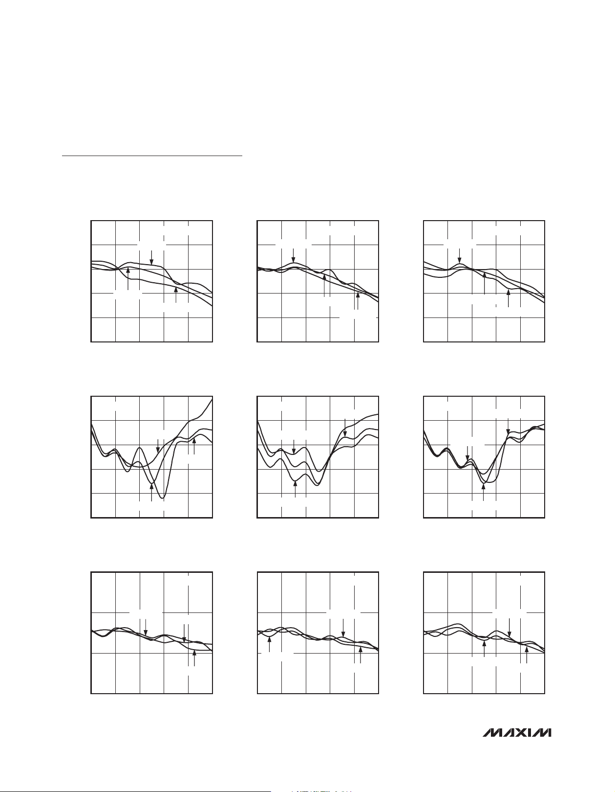
Typical Operating Characteristics
(Typical Application Circuit with tuning elements outlined in Table 1, Downconverter Mode, VCC = 5.0V, fRF = 3000MHz to
4000MHz, LO is low-side injected for a 300MHz IF, PRF = 0dBm, PLO = 0dBm, TC = +25NC, unless otherwise noted.)
CONVERSION LOSS vs. RF FREQUENCY
10
9
8
CONVERSION LOSS (dB)
7
6
TC = +85°C
3000 4000
RF FREQUENCY (MHz)
T
C
TC = +25°C
= -40°C
_______________________________________________________________________________________ 9
MAX2044 toc01
3800360034003200
CONVERSION LOSS vs. RF FREQUENCY
10
9
8
CONVERSION LOSS (dB)
7
6
3000 4000
PLO = -3dBm, 0dBm, +3dBm
RF FREQUENCY (MHz)
CONVERSION LOSS vs. RF FREQUENCY
10
MAX2044 toc02
9
8
CONVERSION LOSS (dB)
7
3800360034003200
6
3000 4000
VCC = 4.75V, 5.0V, 5.25V
3800360034003200
RF FREQUENCY (MHz)
MAX2044 toc03
Page 10
SiGe, High-Linearity, 2300MHz to 4000MHz
Upconversion/Downconversion Mixer with LO Buffer
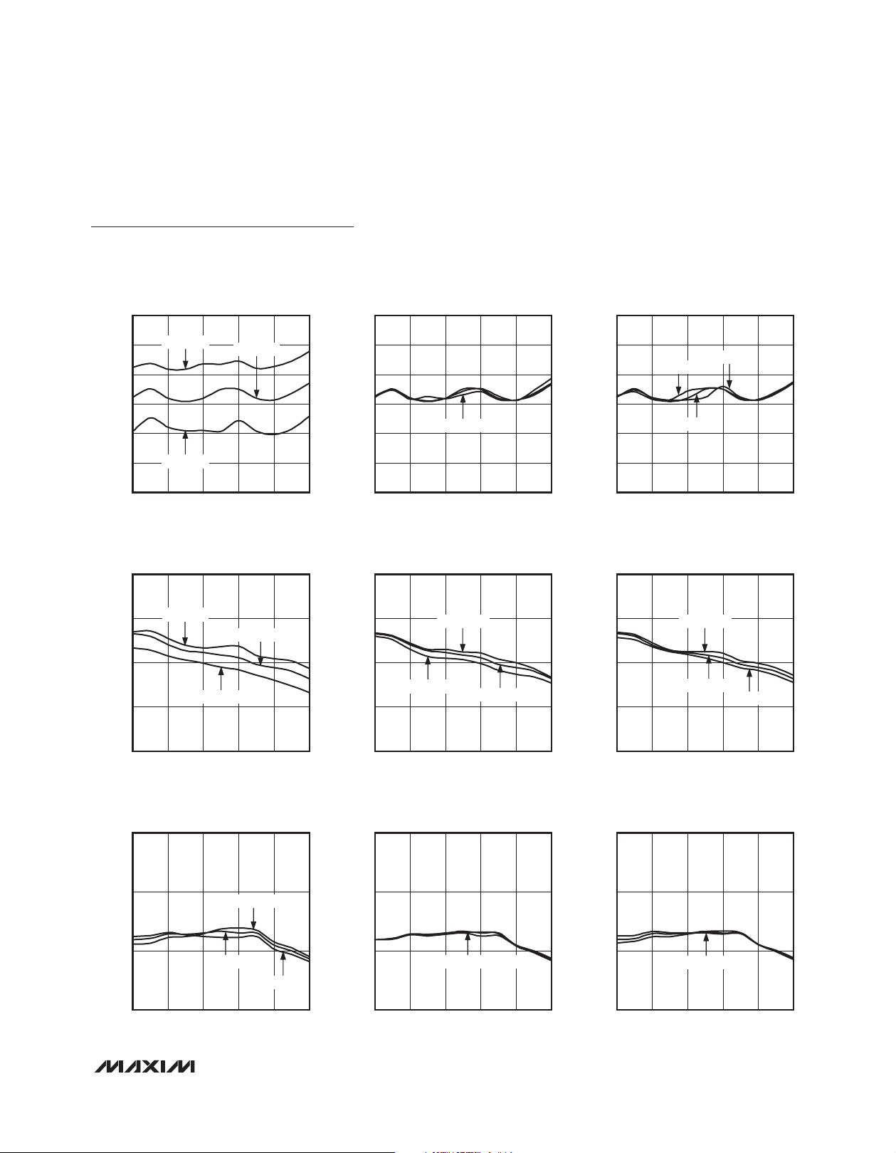
Typical Operating Characteristics (continued)
(Typical Application Circuit with tuning elements outlined in Table 1, Downconverter Mode, VCC = 5.0V, fRF = 3000MHz to
4000MHz, LO is low-side injected for a 300MHz IF, PRF = 0dBm, PLO = 0dBm, TC = +25NC, unless otherwise noted.)
INPUT IP3 vs. RF FREQUENCY
37
MAX2044
35
33
31
INPUT IP3 (dBm)
29
27
75
70
65
60
2RF - 2LO RESPONSE (dBc)
55
50
TC = +25°C
3000 4000
RF FREQUENCY (MHz)
2RF - 2LO RESPONSE vs. RF FREQUENCY
PRF = 0dBm
3000 4000
RF FREQUENCY (MHz)
= -40°C
T
C
TC = +85°C
TC = +25°C
P
= 0dBm/TONE
RF
TC = +85°C
3800360034003200
T
3800360034003200
= -40°C
C
37
MAX2044 toc04
35
33
31
INPUT IP3 (dBm)
29
27
3000 4000
2RF - 2LO RESPONSE vs. RF FREQUENCY
75
MAX2044 toc07
70
65
60
2RF - 2LO RESPONSE (dBc)
55
50
3000 4000
INPUT IP3 vs. RF FREQUENCY
P
RF
P
= +3dBm
LO
PLO = 0dBm
RF FREQUENCY (MHz)
PRF = 0dBm
PLO = +3dBm
PLO = -3dBm
RF FREQUENCY (MHz)
P
LO
= 0dBm/TONE
PLO = -3dBm
3800360034003200
= 0dBm
3800360034003200
37
MAX2044 toc05
35
33
31
INPUT IP3 (dBm)
29
27
2RF - 2LO RESPONSE vs. RF FREQUENCY
75
MAX2044 toc08
70
65
60
2RF - 2LO RESPONSE (dBc)
55
50
3000 4000
INPUT IP3 vs. RF FREQUENCY
P
RF
V
= 5.25V
CC
VCC = 5.0V
VCC = 4.75V
RF FREQUENCY (MHz)
PRF = 0dBm
VCC = 4.75V
VCC = 5.0V
RF FREQUENCY (MHz)
V
CC
= 5.25V
= 0dBm/TONE
MAX2044 toc06
38003600340032003000 4000
MAX2044 toc09
3800360034003200
3RF - 3LO RESPONSE vs. RF FREQUENCY
85
75
65
3RF - 3LO RESPONSE (dBc)
55
3000 4000
T
= -40°C
C
RF FREQUENCY (MHz)
PRF = 0dBm
TC = +25°C
MAX2044 toc10
TC = +85°C
3800360034003200
3RF - 3LO RESPONSE vs. RF FREQUENCY
85
75
65
= 0dBm
P
3RF - 3LO RESPONSE (dBc)
LO
55
3000 4000
RF FREQUENCY (MHz)
PRF = 0dBm
PLO = +3dBm
PLO = -3dBm
3RF - 3LO RESPONSE vs. RF FREQUENCY
85
MAX2044 toc11
75
65
3RF - 3LO RESPONSE (dBc)
3800360034003200
55
3000 4000
RF FREQUENCY (MHz)
10 _____________________________________________________________________________________
PRF = 0dBm
MAX2044 toc12
VCC = 5.25V
V
= 5.0V
CC
VCC = 4.75V
3800360034003200
Page 11
SiGe, High-Linearity, 2300MHz to 4000MHz
Upconversion/Downconversion Mixer with LO Buffer
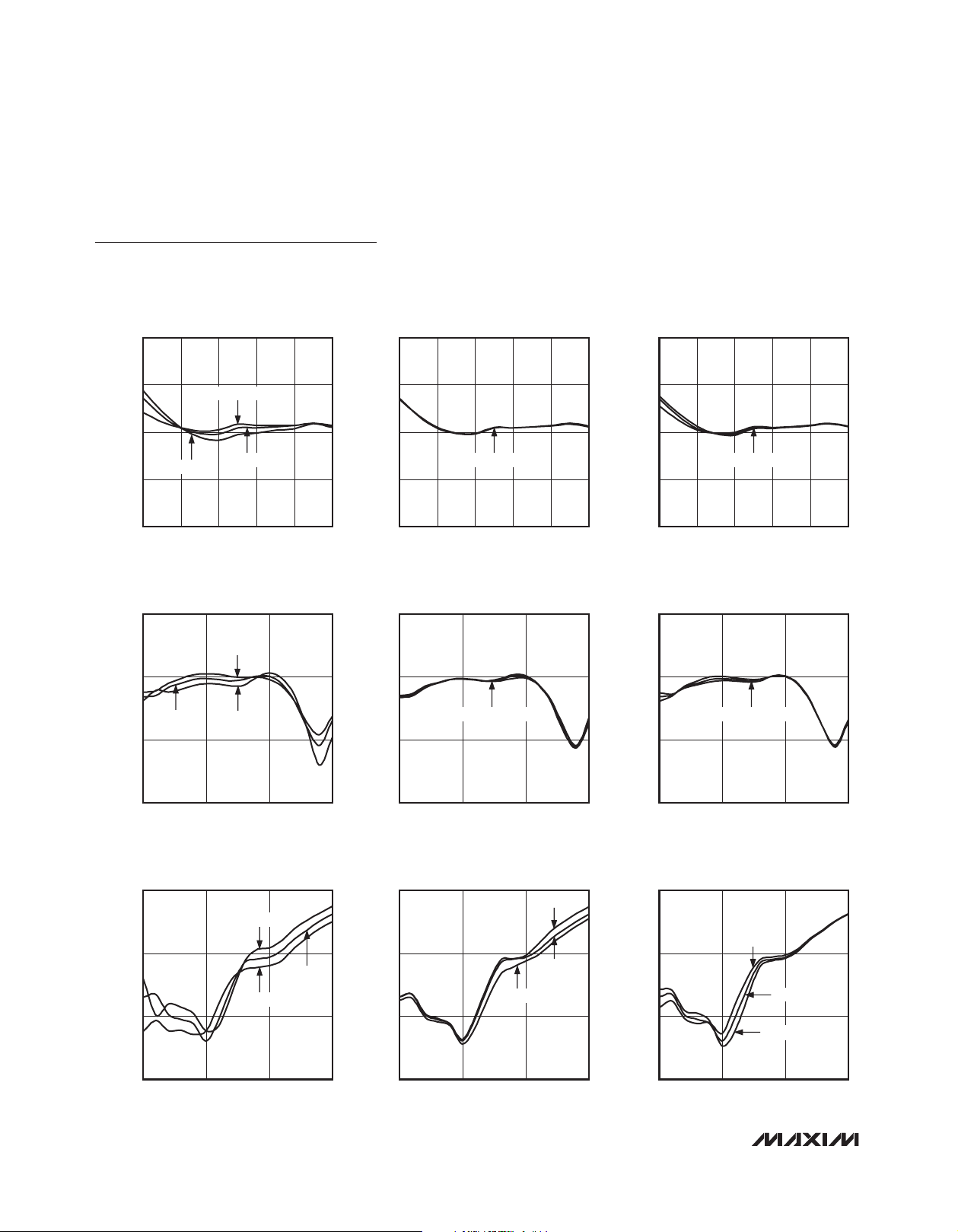
Typical Operating Characteristics (continued)
(Typical Application Circuit with tuning elements outlined in Table 1, Downconverter Mode, VCC = 5.0V, fRF = 3000MHz to
4000MHz, LO is low-side injected for a 300MHz IF, PRF = 0dBm, PLO = 0dBm, TC = +25NC, unless otherwise noted.)
MAX2044
NOISE FIGURE vs. RF FREQUENCY
11
10
9
8
NOISE FIGURE (dB)
7
6
5
25
23
(dBm)
1dB
21
INPUT P
19
TC = +85°C
T
= -40°C
C
RF FREQUENCY (MHz)
INPUT P
TC = -40°C
1dB
TC = +85°C
TC = +25°C
38003600340032003000 4000
vs. RF FREQUENCY
TC = +25°C
MAX2044 toc13
NOISE FIGURE (dB)
MAX2044 toc16
(dBm)
1dB
INPUT P
NOISE FIGURE vs. RF FREQUENCY
11
10
9
8
7
6
5
25
23
21
19
PLO = -3dBm, 0dBm, +3dBm
RF FREQUENCY (MHz)
INPUT P
1dB
PLO = +3dBm
PLO = -3dBm
vs. RF FREQUENCY
38003600340032003000 4000
PLO = 0dBm
MAX2044 toc14
NOISE FIGURE (dB)
MAX2044 toc17
(dBm)
1dB
INPUT P
NOISE FIGURE vs. RF FREQUENCY
11
10
V
9
8
7
6
5
CC
RF FREQUENCY (MHz)
INPUT P
25
23
21
19
VCC = 5.25V
= 4.75V
VCC = 5.0V
vs. RF FREQUENCY
1dB
VCC = 5.25V
VCC = 5.0V
MAX2044 toc15
38003600340032003000 4000
MAX2044 toc18
VCC = 4.75V
17
3000 4000
RF FREQUENCY (MHz)
LO LEAKAGE AT IF PORT
vs. LO FREQUENCY
-10
-20
-30
LO LEAKAGE AT IF PORT (dBm)
-40
2700 3700
LO FREQUENCY (MHz)
TC = +25°C
T
= -40°C
C
______________________________________________________________________________________ 11
3800360034003200
TC = +85°C
3500330031002900
17
3000 4000
-10
MAX2044 toc19
-20
-30
LO LEAKAGE AT IF PORT (dBm)
-40
2700 3700
3800360034003200
RF FREQUENCY (MHz)
LO LEAKAGE AT IF PORT
vs. LO FREQUENCY
PLO = -3dBm, 0dBm, +3dBm
3500330031002900
LO FREQUENCY (MHz)
17
3000 4000
-10
MAX2044 toc20
-20
-30
LO LEAKAGE AT IF PORT (dBm)
-40
2700 3700
3800360034003200
RF FREQUENCY (MHz)
LO LEAKAGE AT IF PORT
vs. LO FREQUENCY
MAX2044 toc21
VCC = 4.75V, 5.0V, 5.25V
3500330031002900
LO FREQUENCY (MHz)
Page 12
SiGe, High-Linearity, 2300MHz to 4000MHz
Upconversion/Downconversion Mixer with LO Buffer
Typical Operating Characteristics (continued)
(Typical Application Circuit with tuning elements outlined in Table 1, Downconverter Mode, VCC = 5.0V, fRF = 3000MHz to
4000MHz, LO is low-side injected for a 300MHz IF, PRF = 0dBm, PLO = 0dBm, TC = +25NC, unless otherwise noted.)
RF-TO-IF ISOLATION vs. RF FREQUENCY
60
MAX2044
50
40
RF-TO-IF ISOLATION (dB)
30
20
-20
-30
-40
LO LEAKAGE AT RF PORT (dBm)
TC = -40°C
3000 4000
RF FREQUENCY (MHz)
LO LEAKAGE AT RF PORT
vs. LO FREQUENCY
TC = +25°C
= +85°C
T
C
TC = +25°C
T
= +85°C
C
TC = -40°C
RF-TO-IF ISOLATION vs. RF FREQUENCY
60
MAX2044 toc22
50
40
RF-TO-IF ISOLATION (dB)
30
3800360034003200
20
3000 4000
PLO = -3dBm, 0dBm, +3dBm
3800360034003200
RF FREQUENCY (MHz)
MAX2044 toc23
LO LEAKAGE AT RF PORT
vs. LO FREQUENCY
-20
MAX2044 toc25
-30
PLO = -3dBm, 0dBm, +3dBm
-40
LO LEAKAGE AT RF PORT (dBm)
MAX2044 toc26
RF-TO-IF ISOLATION vs. RF FREQUENCY
60
50
40
RF-TO-IF ISOLATION (dB)
30
20
3000 4000
VCC = 4.75V, 5.0V, 5.25V
RF FREQUENCY (MHz)
LO LEAKAGE AT RF PORT
vs. LO FREQUENCY
-20
-30
VCC = 4.75V, 5.0V, 5.25V
-40
LO LEAKAGE AT RF PORT (dBm)
MAX2044 toc24
3800360034003200
MAX2044 toc27
-50
2500 4000
3000 3500
LO FREQUENCY (MHz)
2LO LEAKAGE AT RF PORT
vs. LO FREQUENCY
-20
T
= -40°C
C
-30
TC = +85°C
-40
2LO LEAKAGE AT RF PORT (dBm)
-50
2500 4000
3000 3500
LO FREQUENCY (MHz)
TC = +25°C
-50
2500 4000
-20
MAX2044 toc28
-30
-40
2LO LEAKAGE AT RF PORT (dBm)
-50
2500 4000
3000 3500
LO FREQUENCY (MHz)
2LO LEAKAGE AT RF PORT
vs. LO FREQUENCY
= +3dBm
P
LO
PLO = 0dBm
PLO = -3dBm
3000 3500
LO FREQUENCY (MHz)
-50
2500 4000
-20
MAX2044 toc29
-30
-40
2LO LEAKAGE AT RF PORT (dBm)
-50
2500 4000
3000 3500
LO FREQUENCY (MHz)
2LO LEAKAGE AT RF PORT
vs. LO FREQUENCY
3000 3500
LO FREQUENCY (MHz)
12 _____________________________________________________________________________________
VCC = 4.75V
MAX2044 toc30
VCC = 5.0V
VCC = 5.25V
Page 13

SiGe, High-Linearity, 2300MHz to 4000MHz
Upconversion/Downconversion Mixer with LO Buffer
Typical Operating Characteristics (continued)
(Typical Application Circuit with tuning elements outlined in Table 1, Downconverter Mode, VCC = 5.0V, fRF = 3000MHz to
4000MHz, LO is low-side injected for a 300MHz IF, PRF = 0dBm, PLO = 0dBm, TC = +25NC, unless otherwise noted.)
MAX2044
RF PORT RETURN LOSS
vs. RF FREQUENCY
0
5
10
15
20
RF PORT RETURN LOSS (dB)
25
30
RF FREQUENCY (MHz)
LO PORT RETURN LOSS
vs. LO FREQUENCY
0
10
20
LO PORT RETURN LOSS (dB)
PLO = 0dBm
= 300MHz
f
IF
PLO = -3dBm, 0dBm, +3dBm
38003600340032003000 4000
PLO = -3dBm
PLO = +3dBm
MAX2044 toc31
MAX2044 toc33
IF PORT RETURN LOSS
vs. IF FREQUENCY
0
5
10
15
20
IF PORT RETURN LOSS (dB)
25
30
VCC = 4.75V, 5.0V, 5.25V
IF FREQUENCY (MHz)
SUPPLY CURRENT
vs. TEMPERATURE (T
150
145
140
135
= 4.75V
130
SUPPLY CURRENT (mA)
125
V
CC
VCC = 5.25V
fLO = 3200MHz
C
VCC = 5.0V
MAX2044 toc32
41032023014050 500
)
MAX2044 toc34
30
2500 4000
3000 3500
LO FREQUENCY (MHz)
120
603510-15-40 85
TEMPERATURE (°C)
______________________________________________________________________________________ 13
Page 14

SiGe, High-Linearity, 2300MHz to 4000MHz
Upconversion/Downconversion Mixer with LO Buffer
Typical Operating Characteristics (continued)
(Typical Application Circuit with tuning elements outlined in Table 1, Downconverter Mode, VCC = 3.3V, fRF = 3000MHz to
4000MHz, LO is low-side injected for a 300MHz IF, PRF = 0dBm, PLO = 0dBm, TC = +25NC, unless otherwise noted.)
CONVERSION LOSS vs. RF FREQUENCY
10
MAX2044
9
8
CONVERSION LOSS (dB)
7
6
34
32
30
28
INPUT IP3 (dBm)
26
TC = +85°C
3000 4000
RF FREQUENCY (MHz)
INPUT IP3 vs. RF FREQUENCY
= +85°C
T
C
TC = +25°C
TC = -40°C
TC = -40°C
TC = +25°C
3800360034003200
P
= 0dBm/TONE
RF
VCC = 3.3V
V
= 3.3V
CC
10
MAX2044 toc35
MAX2044 toc38
9
8
CONVERSION LOSS (dB)
7
6
34
32
30
28
INPUT IP3 (dBm)
26
CONVERSION LOSS vs. RF FREQUENCY
VCC = 3.3V
PLO = -3dBm, 0dBm, +3dBm
3000 4000
RF FREQUENCY (MHz)
3800360034003200
INPUT IP3 vs. RF FREQUENCY
= 3.3V
V
CC
P
= 0dBm/TONE
RF
PLO = -3dBm, 0dBm, +3dBm
10
MAX2044 toc36
MAX2044 toc39
9
8
CONVERSION LOSS (dB)
7
6
34
32
30
28
INPUT IP3 (dBm)
26
CONVERSION LOSS vs. RF FREQUENCY
VCC = 3.0V, 3.3V, 3.6V
3000 4000
RF FREQUENCY (MHz)
3800360034003200
INPUT IP3 vs. RF FREQUENCY
P
= 0dBm/TONE
V
= 3.6V
CC
VCC = 3.3V
RF
VCC = 3.0V
MAX2044 toc37
MAX2044 toc40
24
3000 4000
RF FREQUENCY (MHz)
2RF - 2LO RESPONSE vs. RF FREQUENCY
80
VCC = 3.3V
P
= 0dBm
RF
70
TC = +85°C
60
2RF - 2LO RESPONSE (dBc)
TC = +25°C
50
3000 4000
RF FREQUENCY (MHz)
T
= -40°C
C
3800360034003200
3800360034003200
24
3000 4000
2RF - 2LO RESPONSE vs. RF FREQUENCY
80
MAX2044 toc41
70
60
2RF - 2LO RESPONSE (dBc)
50
3000 4000
VCC = 3.3V
P
= 0dBm
RF
PLO = -3dBm
RF FREQUENCY (MHz)
PLO = +3dBm
PLO = 0dBm
RF FREQUENCY (MHz)
3800360034003200
24
RF FREQUENCY (MHz)
2RF - 2LO RESPONSE vs. RF FREQUENCY
80
PRF = 0dBm
MAX2044 toc42
70
VCC = 3.3V
60
2RF - 2LO RESPONSE (dBc)
3800360034003200
50
3000 4000
RF FREQUENCY (MHz)
14 _____________________________________________________________________________________
38003600340032003000 4000
MAX2044 toc43
VCC = 3.6V
VCC = 3.0V
3800360034003200
Page 15

SiGe, High-Linearity, 2300MHz to 4000MHz
Upconversion/Downconversion Mixer with LO Buffer
Typical Operating Characteristics (continued)
(Typical Application Circuit with tuning elements outlined in Table 1, Downconverter Mode, VCC = 3.3V, fRF = 3000MHz to
4000MHz, LO is low-side injected for a 300MHz IF, PRF = 0dBm, PLO = 0dBm, TC = +25NC, unless otherwise noted.)
MAX2044
3RF - 3LO RESPONSE vs. RF FREQUENCY
75
TC = +25°C
65
TC = -40°C
55
3RF - 3LO RESPONSE (dBc)
45
3000 4000
RF FREQUENCY (MHz)
VCC = 3.3V
P
NOISE FIGURE vs. RF FREQUENCY
11
10
9
8
NOISE FIGURE (dB)
7
6
TC = +85°C
T
= -40°C
C
TC = +25°C
= 0dBm
RF
TC = +85°C
3800360034003200
= 3.3V
V
CC
3RF - 3LO RESPONSE vs. RF FREQUENCY
75
MAX2044 toc44
65
55
3RF - 3LO RESPONSE (dBc)
45
3000 4000
11
10
MAX2044 toc47
9
8
NOISE FIGURE (dB)
7
6
VCC = 3.3V
P
= 0dBm
RF
PLO = -3dBm, 0dBm, +3dBm
3800360034003200
RF FREQUENCY (MHz)
NOISE FIGURE vs. RF FREQUENCY
= 3.3V
V
CC
PLO = -3dBm
P
LO
PLO = 0dBm
= +3dBm
3RF - 3LO RESPONSE vs. RF FREQUENCY
75
MAX2044 toc45
65
55
3RF - 3LO RESPONSE (dBc)
45
3000 4000
11
10
MAX2044 toc48
9
8
NOISE FIGURE (dB)
7
6
PRF = 0dBm
VCC = 3.6V
VCC = 3.0V
RF FREQUENCY (MHz)
VCC = 3.3V
3800360034003200
NOISE FIGURE vs. RF FREQUENCY
VCC = 3.0V
VCC = 3.3V
V
= 3.6V
CC
MAX2044 toc46
MAX2044 toc49
23
21
(dBm)
1dB
19
INPUT P
17
15
5
RF FREQUENCY (MHz)
INPUT P
= -40°C
T
C
vs. RF FREQUENCY
1dB
TC = +25°C
TC = +85°C
RF FREQUENCY (MHz)
38003600340032003000 4000
VCC = 3.3V
MAX2044 toc50
38003600340032003000 4000
5
RF FREQUENCY (MHz)
INPUT P
23
21
(dBm)
1dB
19
INPUT P
17
15
3000 4000
vs. RF FREQUENCY
1dB
PLO = -3dBm, 0dBm, +3dBm
RF FREQUENCY (MHz)
38003600340032003000 4000
VCC = 3.3V
3800360034003200
MAX2044 toc51
5
RF FREQUENCY (MHz)
INPUT P
23
21
(dBm)
1dB
19
INPUT P
17
15
3000 4000
vs. RF FREQUENCY
1dB
V
= 3.6V
CC
VCC = 3.3V
RF FREQUENCY (MHz)
VCC = 3.0V
38003600340032003000 4000
MAX2044 toc52
3800360034003200
______________________________________________________________________________________ 15
Page 16

SiGe, High-Linearity, 2300MHz to 4000MHz
Upconversion/Downconversion Mixer with LO Buffer
Typical Operating Characteristics (continued)
(Typical Application Circuit with tuning elements outlined in Table 1, Downconverter Mode, VCC = 3.3V, fRF = 3000MHz to
4000MHz, LO is low-side injected for a 300MHz IF, PRF = 0dBm, PLO = 0dBm, TC = +25NC, unless otherwise noted.)
LO LEAKAGE AT IF PORT
vs. LO FREQUENCY
-10
MAX2044
-20
-30
LO LEAKAGE AT IF PORT (dBm)
-40
60
50
40
RF-TO-IF ISOLATION (dB)
30
T
= -40°C
C
2700 3700
LO FREQUENCY (MHz)
RF-TO-IF ISOLATION vs. RF FREQUENCY
TC = -40°C
TC = +85°C
TC = +85°C
VCC = 3.3V
TC = +25°C
VCC = 3.3V
TC = +25°C
LO LEAKAGE AT IF PORT
vs. LO FREQUENCY
-10
MAX2044 toc53
-20
PLO = -3dBm, 0dBm, +3dBm
-30
LO LEAKAGE AT IF PORT (dBm)
3500330031002900
-40
2700 3700
LO FREQUENCY (MHz)
VCC = 3.3V
3500330031002900
-10
MAX2044 toc54
-20
-30
LO LEAKAGE AT IF PORT (dBm)
-40
RF-TO-IF ISOLATION vs. RF FREQUENCY
60
MAX2044 toc56
50
40
RF-TO-IF ISOLATION (dB)
30
VCC = 3.3V
PLO = -3dBm, 0dBm, +3dBm
60
MAX2044 toc57
50
40
RF-TO-IF ISOLATION (dB)
30
LO LEAKAGE AT IF PORT
vs. LO FREQUENCY
VCC = 3.0V, 3.3V, 3.6V
2700 3700
LO FREQUENCY (MHz)
3500330031002900
RF-TO-IF ISOLATION vs. RF FREQUENCY
VCC = 3.0V, 3.3V, 3.6V
MAX2044 toc55
MAX2044 toc58
20
3000 4000
RF FREQUENCY (MHz)
LO LEAKAGE AT RF PORT
vs. LO FREQUENCY
-20
-30
TC = -40°C, +25°C, +85°C
-40
LO LEAKAGE AT RF PORT (dBm)
-50
2500 4000
3000 3500
LO FREQUENCY (MHz)
3800360034003200
= 3.3V
V
CC
20
3000 4000
-20
MAX2044 toc59
-30
-40
LO LEAKAGE AT RF PORT (dBm)
-50
2500 4000
3800360034003200
RF FREQUENCY (MHz)
LO LEAKAGE AT RF PORT
vs. LO FREQUENCY
V
PLO = -3dBm, 0dBm, +3dBm
3000 3500
LO FREQUENCY (MHz)
CC
= 3.3V
20
3000 4000
-20
MAX2044 toc60
-30
-40
LO LEAKAGE AT RF PORT (dBm)
-50
2500 4000
RF FREQUENCY (MHz)
LO LEAKAGE AT RF PORT
vs. LO FREQUENCY
VCC = 3.0V, 3.3V, 3.6V
3000 3500
LO FREQUENCY (MHz)
16 _____________________________________________________________________________________
3800360034003200
MAX2044 toc61
Page 17

SiGe, High-Linearity, 2300MHz to 4000MHz
Upconversion/Downconversion Mixer with LO Buffer
Typical Operating Characteristics (continued)
(Typical Application Circuit with tuning elements outlined in Table 1, Downconverter Mode, VCC = 3.3V, fRF = 3000MHz to
4000MHz, LO is low-side injected for a 300MHz IF, PRF = 0dBm, PLO = 0dBm, TC = +25NC, unless otherwise noted.)
MAX2044
2LO LEAKAGE AT RF PORT
vs. LO FREQUENCY
-15
-25
-35
-45
2LO LEAKAGE AT RF PORT (dBm)
-55
2500 4000
TC = -40°C
T
LO FREQUENCY (MHz)
= +85°C
C
VCC = 3.3V
35003000
RF PORT RETURN LOSS
vs. RF FREQUENCY
0
5
10
15
20
RF PORT RETURN LOSS (dB)
25
30
MAX2044 toc62
TC = +25°C
PLO = -3dBm, 0dBm, +3dBm
RF FREQUENCY (MHz)
2LO LEAKAGE AT RF PORT
vs. LO FREQUENCY
-15
-25
-35
-45
2LO LEAKAGE AT RF PORT (dBm)
-55
2500 4000
= 3.3V
V
CC
f
= 300MHz
IF
38003600340032003000 4000
MAX2044 toc65
PLO = -3dBm, 0dBm, +3dBm
LO FREQUENCY (MHz)
VCC = 3.3V
35003000
IF PORT RETURN LOSS (dB)
0
5
10
15
VCC = 3.0V, 3.3V, 3.6V
20
25
30
-15
MAX2044 toc63
-25
VCC = 3.3V
-35
-45
2LO LEAKAGE AT RF PORT (dBm)
-55
2500 4000
IF PORT RETURN LOSS
vs. IF FREQUENCY
IF FREQUENCY (MHz)
2LO LEAKAGE AT RF PORT
vs. LO FREQUENCY
= 3.0V
V
CC
VCC = 3.6V
35003000
LO FREQUENCY (MHz)
f
= 3200MHz
LO
MAX2044 toc66
41032023014050 500
MAX2044 toc64
LO PORT RETURN LOSS
vs. LO FREQUENCY
0
10
20
LO PORT RETURN LOSS (dB)
30
2500 4000
= -3dBm
P
LO
PLO = +3dBm
3000 3500
LO FREQUENCY (MHz)
PLO = 0dBm
VCC = 3.3V
MAX2044 toc67
135
130
125
120
115
SUPPLY CURRENT (mA)
110
105
SUPPLY CURRENT
vs.TEMPERATURE (T
VCC = 3.6V
VCC = 3.3V
V
= 3.0V
CC
TEMPERATURE (°C)
)
C
603510-15-40 85
MAX2044 toc68
______________________________________________________________________________________ 17
Page 18

SiGe, High-Linearity, 2300MHz to 4000MHz
Upconversion/Downconversion Mixer with LO Buffer
Typical Operating Characteristics (continued)
(Typical Application Circuit with tuning elements outlined in Table 1, Downconverter Mode, VCC = 5.0V, fRF = 2300MHz to
2900MHz, LO is high-side injected for a 300MHz IF, PRF = 0dBm, PLO = 0dBm, TC = +25NC, unless otherwise noted.)
CONVERSION LOSS vs. RF FREQUENCY
10
MAX2044
9
8
CONVERSION LOSS (dB)
7
6
TC = +85°C
TC = -40°C
2300 2900
RF FREQUENCY (MHz)
INPUT IP3 vs. RF FREQUENCY
37
PRF = 0dBm/TONE
35
33
31
INPUT IP3 (dBm)
TC = +85°C
TC = +25°C
TC = -40°C
TC = +25°C
CONVERSION LOSS vs. RF FREQUENCY
10
MAX2044 toc69
275026002450
9
8
CONVERSION LOSS (dB)
PLO = -3dBm, 0dBm, +3dBm
7
6
2300 2900
RF FREQUENCY (MHz)
275026002450
MAX2044 toc70
INPUT IP3 vs. RF FREQUENCY
37
MAX2044 toc72
PRF = 0dBm/TONE
35
33
31
INPUT IP3 (dBm)
PLO = -3dBm
PLO = +3dBm
MAX2044 toc73
PLO = 0dBm
CONVERSION LOSS vs. RF FREQUENCY
10
9
8
CONVERSION LOSS (dB)
7
6
VCC = 4.75V, 5.0V, 5.25V
2300 2900
RF FREQUENCY (MHz)
275026002450
INPUT IP3 vs. RF FREQUENCY
37
PRF = 0dBm/TONE
35
VCC = 5.25V
33
31
INPUT IP3 (dBm)
VCC = 4.75V
VCC = 5.0V
MAX2044 toc71
MAX2044 toc74
29
27
2300 2900
RF FREQUENCY (MHz)
275026002450
2LO - 2RF RESPONSE
vs. RF FREQUENCY
80
PRF = 0dBm
TC = +85°C
70
60
2LO - 2RF RESPONSE (dBc)
TC = -40°C
50
2300 2900
TC = +25°C
275026002450
RF FREQUENCY (MHz)
29
27
2300 2900
80
MAX2044 toc75
70
60
2LO - 2RF RESPONSE (dBc)
50
2300 2900
RF FREQUENCY (MHz)
2LO - 2RF RESPONSE
vs. RF FREQUENCY
PRF = 0dBm
PLO = -3dBm
RF FREQUENCY (MHz)
275026002450
PLO = +3dBm
PLO = 0dBm
275026002450
29
27
2300 2900
80
MAX2044 toc76
70
60
2LO - 2RF RESPONSE (dBc)
50
2300 2900
RF FREQUENCY (MHz)
2LO - 2RF RESPONSE
vs. RF FREQUENCY
PRF = 0dBm
RF FREQUENCY (MHz)
18 _____________________________________________________________________________________
275026002450
MAX2044 toc77
VCC = 4.75V
VCC = 5.0V
VCC = 5.25V
275026002450
Page 19

SiGe, High-Linearity, 2300MHz to 4000MHz
Upconversion/Downconversion Mixer with LO Buffer
Typical Operating Characteristics (continued)
(Typical Application Circuit with tuning elements outlined in Table 1, Downconverter Mode, VCC = 5.0V, fRF = 2300MHz to
2900MHz, LO is high-side injected for a 300MHz IF, PRF = 0dBm, PLO = 0dBm, TC = +25NC, unless otherwise noted.)
MAX2044
3LO - 3RF RESPONSE
vs. RF FREQUENCY
85
PRF = 0dBm
TC = +85°C
75
65
3LO - 3RF RESPONSE (dBc)
55
2300 2900
TC = +25°C
TC = -40°C
275026002450
RF FREQUENCY (MHz)
LO LEAKAGE AT IF PORT
vs. LO FREQUENCY
-20
-25
TC = +85°C
-30
-35
LO LEAKAGE AT IF PORT (dBm)
TC = -40°C
TC = +25°C
85
PRF = 0dBm
MAX2044 toc78
75
65
3LO - 3RF RESPONSE (dBc)
55
2300 2900
-20
MAX2044 toc81
-25
-30
-35
LO LEAKAGE AT IF PORT (dBm)
3LO - 3RF RESPONSE
vs. RF FREQUENCY
PLO = +3dBm
PLO = 0dBm
RF FREQUENCY (MHz)
PLO = -3dBm
275026002450
LO LEAKAGE AT IF PORT
vs. LO FREQUENCY
PLO = -3dBm, 0dBm, +3dBm
85
PRF = 0dBm
MAX2044 toc79
75
65
3LO - 3RF RESPONSE (dBc)
55
2300 2900
-20
MAX2044 toc82
-25
-30
-35
LO LEAKAGE AT IF PORT (dBm)
VCC = 5.25V
3LO - 3RF RESPONSE
vs. RF FREQUENCY
VCC = 5.25V
VCC = 5.0V
VCC = 4.75V
RF FREQUENCY (MHz)
LO LEAKAGE AT IF PORT
vs. LO FREQUENCY
VCC = 4.75V
VCC = 5.0V
MAX2044 toc80
275026002450
MAX2044 toc83
-40
2600 3200
LO FREQUENCY (MHz)
305029002750
RF-TO-IF ISOLATION vs. RF FREQUENCY
60
50
40
RF-TO-IF ISOLATION (dB)
30
20
2300 2900
TC = -40°C
TC = +25°C
RF FREQUENCY (MHz)
TC = +85°C
275026002450
______________________________________________________________________________________ 19
-40
2600 3200
60
MAX2044 toc84
50
40
RF-TO-IF ISOLATION (dB)
30
20
2300 2900
305029002750
LO FREQUENCY (MHz)
RF-TO-IF ISOLATION vs. RF FREQUENCY
PLO = -3dBm, 0dBm, +3dBm
275026002450
RF FREQUENCY (MHz)
-40
60
MAX2044 toc85
50
40
RF-TO-IF ISOLATION (dB)
30
20
2600 3200
LO FREQUENCY (MHz)
305029002750
RF-TO-IF ISOLATION vs. RF FREQUENCY
VCC = 4.75V, 5.0V, 5.25V
2300 2900
RF FREQUENCY (MHz)
275026002450
MAX2044 toc86
Page 20

SiGe, High-Linearity, 2300MHz to 4000MHz
Upconversion/Downconversion Mixer with LO Buffer
Typical Operating Characteristics (continued)
(Typical Application Circuit with tuning elements outlined in Table 1, Downconverter Mode, VCC = 5.0V, fRF = 2300MHz to
2900MHz, LO is high-side injected for a 300MHz IF, PRF = 0dBm, PLO = 0dBm, TC = +25NC, unless otherwise noted.)
LO LEAKAGE AT RF PORT
vs. LO FREQUENCY
-20
MAX2044
-30
-40
LO LEAKAGE AT RF PORT (dBm)
-50
TC = +85°C
TC = -40°C
2300 4000
TC = +25°C
LO FREQUENCY (MHz)
2LO LEAKAGE AT RF PORT
vs. LO FREQUENCY
-20
-30
-40
TC = +25°C
TC = -40°C
LO LEAKAGE AT RF PORT
vs. LO FREQUENCY
-20
MAX2044 toc87
-30
PLO = -3dBm, 0dBm, +3dBm
-40
LO LEAKAGE AT RF PORT (dBm)
357531502725
-50
2300 4000
LO FREQUENCY (MHz)
357531502725
-20
MAX2044 toc88
-30
-40
LO LEAKAGE AT RF PORT (dBm)
-50
2LO LEAKAGE AT RF PORT
vs. LO FREQUENCY
MAX2044 toc90
-20
-30
-40
PLO = +3dBm
PLO = 0dBm
-20
MAX2044 toc91
-30
-40
LO LEAKAGE AT RF PORT
vs. LO FREQUENCY
VCC = 4.75V, 5.0V, 5.25V
2300 4000
LO FREQUENCY (MHz)
357531502725
2LO LEAKAGE AT RF PORT
vs. LO FREQUENCY
VCC = 5.25V
VCC = 5.0V
MAX2044 toc89
MAX2044 toc92
-50
2LO LEAKAGE AT RF PORT (dBm)
-60
2300 4000
LO FREQUENCY (MHz)
TC = +85°C
357531502725
-50
2LO LEAKAGE AT RF PORT (dBm)
-60
2300 4000
LO FREQUENCY (MHz)
PLO = -3dBm
357531502725
-50
2LO LEAKAGE AT RF PORT (dBm)
VCC = 4.75V
-60
2300 4000
LO FREQUENCY (MHz)
20 _____________________________________________________________________________________
357531502725
Page 21

SiGe, High-Linearity, 2300MHz to 4000MHz
Upconversion/Downconversion Mixer with LO Buffer
Typical Operating Characteristics (continued)
(Typical Application Circuit with tuning elements outlined in Table 1, Downconverter Mode, VCC = 5.0V, fRF = 2300MHz to
2900MHz, LO is high-side injected for a 300MHz IF, PRF = 0dBm, PLO = 0dBm, TC = +25NC, unless otherwise noted.)
MAX2044
RF PORT RETURN LOSS
vs. RF FREQUENCY
0
fIF = 300MHz
5
10
15
20
RF PORT RETURN LOSS (dB)
25
30
PLO = -3dBm, 0dBm, +3dBm
2300 2900
RF FREQUENCY (MHz)
275026002450
LO PORT RETURN LOSS
vs. LO FREQUENCY
0
PLO = -3dBm
10
20
PLO = 0dBm
30
LO PORT RETURN LOSS (dB)
PLO = +3dBm
MAX2044 toc93
MAX2044 toc95
IF PORT RETURN LOSS
vs. IF FREQUENCY
0
5
10
15
20
IF PORT RETURN LOSS (dB)
25
30
fLO = 3200MHz
fLO = 2600MHz
50 500
VCC = 4.75V, 5.0V, 5.25V
fLO = 2900MHz
IF FREQUENCY (MHz)
SUPPLY CURRENT
vs. TEMPERATURE (T
150
145
140
135
130
SUPPLY CURRENT (mA)
125
VCC = 5.25V
VCC = 5.0V
VCC = 4.75V
MAX2044 toc94
410320230140
)
C
MAX2044 toc96
40
2500 4000
LO FREQUENCY (MHz)
35003000
120
-40 85
TEMPERATURE (°C)
603510-15
______________________________________________________________________________________ 21
Page 22

SiGe, High-Linearity, 2300MHz to 4000MHz
Upconversion/Downconversion Mixer with LO Buffer
Typical Operating Characteristics (continued)
(Typical Application Circuit with tuning elements outlined in Table 1, Downconverter Mode, VCC = 5.0V, fRF = 3000MHz to
4000MHz, LO is high-side injected for a 300MHz IF, PRF = 0dBm, PLO = 0dBm, TC = +25NC, unless otherwise noted.)
CONVERSION LOSS vs. RF FREQUENCY
10
MAX2044
9
TC = +85°C
8
CONVERSION LOSS (dB)
7
TC = -40°C
6
3000 4000
RF FREQUENCY (MHz)
INPUT IP3 vs. RF FREQUENCY
37
PRF = 0dBm/TONE
35
33
31
INPUT IP3 (dBm)
29
TC = +25°C
TC = -40°C
TC = +25°C
TC = +85°C
CONVERSION LOSS vs. RF FREQUENCY
10
MAX2044 toc97
3800360034003200
9
8
CONVERSION LOSS (dB)
7
6
3000 4000
PLO = -3dBm, 0dBm, +3dBm
RF FREQUENCY (MHz)
3800360034003200
MAX2044 toc98
INPUT IP3 vs. RF FREQUENCY
37
PRF = 0dBm/TONE
MAX2044 toc100
35
33
31
INPUT IP3 (dBm)
PLO = -3dBm
29
PLO = +3dBm
PLO = 0dBm
MAX2044 toc101
CONVERSION LOSS vs. RF FREQUENCY
10
9
8
CONVERSION LOSS (dB)
7
6
3000 4000
VCC = 4.75V, 5.0V, 5.25V
RF FREQUENCY (MHz)
INPUT IP3 vs. RF FREQUENCY
37
PRF = 0dBm/TONE
35
33
31
INPUT IP3 (dBm)
29
VCC = 5.0V
VCC = 4.75V
VCC = 5.25V
MAX2044 toc99
3800360034003200
MAX2044 toc102
27
3000 4000
RF FREQUENCY (MHz)
2LO - 2RF RESPONSE
vs. RF FREQUENCY
80
PRF = 0dBm
70
60
2LO - 2RF RESPONSE (dBc)
50
3000 4000
TC = +85°C
TC = -40°C
RF FREQUENCY (MHz)
TC = +25°C
3800360034003200
3800360034003200
27
3000 4000
80
MAX2044 toc103
70
60
2LO - 2RF RESPONSE (dBc)
50
3000 4000
RF FREQUENCY (MHz)
2LO - 2RF RESPONSE
vs. RF FREQUENCY
PRF = 0dBm
PLO = +3dBm
PLO = -3dBm
RF FREQUENCY (MHz)
3800360034003200
PLO = 0dBm
3800360034003200
27
3000 4000
80
MAX2044 toc104
70
60
2LO - 2RF RESPONSE (dBc)
50
3000 4000
RF FREQUENCY (MHz)
2LO - 2RF RESPONSE
vs. RF FREQUENCY
PRF = 0dBm
VCC = 5.25V
VCC = 5.0V
VCC = 4.75V
RF FREQUENCY (MHz)
22 _____________________________________________________________________________________
3800360034003200
MAX2044 toc105
3800360034003200
Page 23

SiGe, High-Linearity, 3000MHz to 4000MHz
Upconversion/Downconversion Mixer with LO Buffer
Typical Operating Characteristics (continued)
(Typical Application Circuit with tuning elements outlined in Table 1, Downconverter Mode, VCC = 5.0V, fRF = 3000MHz to
4000MHz, LO is high-side injected for a 300MHz IF, PRF = 0dBm, PLO = 0dBm, TC = +25NC, unless otherwise noted.)
MAX2044
3LO - 3RF RESPONSE
vs. RF FREQUENCY
85
PRF = 0dBm
75
65
3LO - 3RF RESPONSE (dBc)
55
3000 4000
TC = -40°C
TC = +25°C
TC = +85°C
RF FREQUENCY (MHz)
LO LEAKAGE AT IF PORT
vs. LO FREQUENCY
-10
-20
TC = -40°C
-30
LO LEAKAGE AT IF PORT (dBm)
-40
3300 4300
TC = +25°C
LO FREQUENCY (MHz)
TC = +85°C
3LO - 3RF RESPONSE
vs. RF FREQUENCY
85
PRF = 0dBm
MAX2044 toc106
75
PLO = +3dBm
65
3LO - 3RF RESPONSE (dBc)
3800360034003200
55
3000 4000
PLO = 0dBm
PLO = -3dBm
3800360034003200
RF FREQUENCY (MHz)
85
MAX2044 toc107
75
65
3LO - 3RF RESPONSE (dBc)
55
3000 4000
LO LEAKAGE AT IF PORT
vs. LO FREQUENCY
-10
MAX2044 toc109
-20
PLO = -3dBm, 0dBm, +3dBm
-30
LO LEAKAGE AT IF PORT (dBm)
4100390037003500
-40
3300 4300
LO FREQUENCY (MHz)
4100390037003500
-10
MAX2044 toc110
-20
-30
LO LEAKAGE AT IF PORT (dBm)
-40
3300 4300
3LO - 3RF RESPONSE
vs. RF FREQUENCY
PRF = 0dBm
MAX2044 toc108
VCC = 5.25V
VCC = 5.0V
VCC = 4.75V
3800360034003200
RF FREQUENCY (MHz)
LO LEAKAGE AT IF PORT
vs. LO FREQUENCY
MAX2044 toc111
VCC = 4.75V, 5.0V, 5.25V
4100390037003500
LO FREQUENCY (MHz)
RF-TO-IF ISOLATION vs. RF FREQUENCY
60
50
TC = +25°C, +85°C
40
RF-TO-IF ISOLATION (dB)
30
20
3000 4000
TC = -40°C
RF FREQUENCY (MHz)
______________________________________________________________________________________ 23
RF-TO-IF ISOLATION vs. RF FREQUENCY
60
MAX2044 toc112
50
40
RF-TO-IF ISOLATION (dB)
30
3800360034003200
20
3000 4000
PLO = -3dBm, 0dBm, +3dBm
3800360034003200
RF FREQUENCY (MHz)
MAX2044 toc113
RF-TO-IF ISOLATION vs. RF FREQUENCY
60
50
40
RF-TO-IF ISOLATION (dB)
30
20
3000 4000
VCC = 4.75V, 5.0V, 5.25V
RF FREQUENCY (MHz)
MAX2044 toc114
3800360034003200
Page 24

SiGe, High-Linearity, 2300MHz to 4000MHz
Upconversion/Downconversion Mixer with LO Buffer
Typical Operating Characteristics (continued)
(Typical Application Circuit with tuning elements outlined in Table 1, Downconverter Mode, VCC = 5.0V, fRF = 3000MHz to
4000MHz, LO is high-side injected for a 300MHz IF, PRF = 0dBm, PLO = 0dBm, TC = +25NC, unless otherwise noted.)
LO LEAKAGE AT RF PORT
vs. LO FREQUENCY
-20
MAX2044
-30
-40
LO LEAKAGE AT RF PORT (dBm)
TC = -40°C
-50
3000 4500
-10
-20
-30
-40
2LO LEAKAGE AT RF PORT (dBm)
-50
3000 4200
3500 4000
LO FREQUENCY (MHz)
2LO LEAKAGE AT RF PORT
vs. LO FREQUENCY
TC = +85°C
LO FREQUENCY (MHz)
TC = +85°C
TC = +25°C
TC = -40°C
38003400
TC = +25°C
-20
MAX2044 toc115
-30
-40
LO LEAKAGE AT RF PORT (dBm)
-50
3000 4500
-10
MAX2044 toc118
-20
-30
-40
2LO LEAKAGE AT RF PORT (dBm)
-50
3000 4200
LO LEAKAGE AT RF PORT
vs. LO FREQUENCY
PLO = -3dBm, 0dBm, +3dBm
3500 4000
LO FREQUENCY (MHz)
2LO LEAKAGE AT RF PORT
vs. LO FREQUENCY
PLO = +3dBm
PLO = 0dBm
PLO = -3dBm
38003400
LO FREQUENCY (MHz)
-20
MAX2044 toc116
-30
-40
LO LEAKAGE AT RF PORT (dBm)
-50
3000 4500
-10
MAX2044 toc119
-20
VCC = 4.75V
-30
-40
2LO LEAKAGE AT RF PORT (dBm)
-50
3000 4200
LO LEAKAGE AT RF PORT
vs. LO FREQUENCY
MAX2044 toc117
VCC = 4.75V, 5.0V, 5.25V
3500 4000
LO FREQUENCY (MHz)
2LO LEAKAGE AT RF PORT
vs. LO FREQUENCY
MAX2044 toc120
VCC = 5.0V
VCC = 5.25V
38003400
LO FREQUENCY (MHz)
24 _____________________________________________________________________________________
Page 25

SiGe, High-Linearity, 2300MHz to 4000MHz
Upconversion/Downconversion Mixer with LO Buffer
Typical Operating Characteristics (continued)
(Typical Application Circuit with tuning elements outlined in Table 1, Downconverter Mode, VCC = 5.0V, fRF = 3000MHz to
4000MHz, LO is high-side injected for a 300MHz IF, PRF = 0dBm, PLO = 0dBm, TC = +25NC, unless otherwise noted.)
MAX2044
RF PORT RETURN LOSS
vs. RF FREQUENCY
0
fIF = 300MHz
5
10
15
20
RF PORT RETURN LOSS (dB)
25
30
3000 4000
PLO = -3dBm, 0dBm, +3dBm
RF FREQUENCY (MHz)
LO PORT RETURN LOSS
vs. LO FREQUENCY
0
PLO = -3dBm
10
20
PLO = +3dBm
30
LO PORT RETURN LOSS (dB)
40
PLO = 0dBm
IF PORT RETURN LOSS
vs. IF FREQUENCY
0
fLO = 3800MHz
MAX2044 toc121
3800360034003200
5
10
15
20
IF PORT RETURN LOSS (dB)
25
30
VCC = 4.75V, 5.0V, 5.25V
50 500
IF FREQUENCY (MHz)
MAX2044 toc122
410320230140
SUPPLY CURRENT
vs. TEMPERATURE (TC)
150
VCC = 5.25V
MAX2044 toc124
VCC = 5.0V
VCC = 4.75V
MAX2044 toc123
145
140
135
130
SUPPLY CURRENT (mA)
125
50
3000 4500
LO FREQUENCY (MHz)
40003500
120
-40 85
TEMPERATURE (°C)
603510-15
______________________________________________________________________________________ 25
Page 26

SiGe, High-Linearity, 2300MHz to 4000MHz
Upconversion/Downconversion Mixer with LO Buffer
Typical Operating Characteristics (continued)
(Typical Application Circuit with tuning elements outlined in Table 2, Upconverter Mode, VCC = 5.0V, fRF = 3000MHz to 4000MHz,
LO is low-side injected, fIF = 200MHz, PIF = 0dBm, PLO = 0dBm, TC = +25NC, unless otherwise noted.)
CONVERSION LOSS vs. RF FREQUENCY
10
MAX2044
9
8
CONVERSION LOSS (dB)
7
6
36
34
32
INPUT IP3 (dBm)
30
TC = +85°C
3000 4000
RF FREQUENCY (MHz)
INPUT IP3 vs. RF FREQUENCY
TC = -40°C
TC = +25°C
TC = +85°C
TC = -40°C
TC = +25°C
3800360034003200
PIF = 0dBm/TONE
10
MAX2044 toc125
MAX2044 toc128
9
8
CONVERSION LOSS (dB)
7
6
36
34
32
INPUT IP3 (dBm)
30
CONVERSION LOSS vs. RF FREQUENCY
PLO = -3dBm, 0dBm, +3dBm
3000 4000
RF FREQUENCY (MHz)
3800360034003200
INPUT IP3 vs. RF FREQUENCY
PIF = 0dBm/TONE
PLO = +3dBm
PLO = 0dBm
PLO = -3dBm
10
MAX2044 toc126
MAX2044 toc129
9
8
CONVERSION LOSS (dB)
7
6
36
34
32
INPUT IP3 (dBm)
30
CONVERSION LOSS vs. RF FREQUENCY
VCC = 4.75V, 5.0V, 5.25V
3000 4000
RF FREQUENCY (MHz)
3800360034003200
INPUT IP3 vs. RF FREQUENCY
PIF = 0dBm/TONE
VCC = 5.25V
VCC = 5.0V
VCC = 4.75V
MAX2044 toc127
MAX2044 toc130
28
3000 4000
RF FREQUENCY (MHz)
LO - 2IF RESPONSE vs. RF FREQUENCY
85
75
65
LO - 2IF RESPONSE (dBc)
55
45
3000 4000
TC = +85°C
TC = -40°C
RF FREQUENCY (MHz)
PIF = 0dBm
TC = +25°C
3800360034003200
3800360034003200
28
3000 4000
85
MAX2044 toc131
75
65
LO - 2IF RESPONSE (dBc)
55
45
3000 4000
3800360034003200
RF FREQUENCY (MHz)
LO - 2IF RESPONSE vs. RF FREQUENCY
PIF = 0dBm
PLO = +3dBm
PLO = 0dBm
PLO = -3dBm
3800360034003200
RF FREQUENCY (MHz)
28
85
MAX2044 toc132
75
65
LO - 2IF RESPONSE (dBc)
55
45
3000 4000
RF FREQUENCY (MHz)
LO - 2IF RESPONSE vs. RF FREQUENCY
VCC = 4.75V
3000 4000
RF FREQUENCY (MHz)
26 _____________________________________________________________________________________
VCC = 5.0V
VCC = 5.25V
3800360034003200
PIF = 0dBm
MAX2044 toc133
3800360034003200
Page 27

SiGe, High-Linearity, 2300MHz to 4000MHz
Upconversion/Downconversion Mixer with LO Buffer
Typical Operating Characteristics (continued)
(Typical Application Circuit with tuning elements outlined in Table 2, Upconverter Mode, VCC = 5.0V, fRF = 3000MHz to 4000MHz,
LO is low-side injected, fIF = 200MHz, PIF = 0dBm, PLO = 0dBm, TC = +25NC, unless otherwise noted.)
MAX2044
LO + 2IF RESPONSE vs. RF FREQUENCY
85
75
65
LO + 2IF RESPONSE (dBc)
TC = +85°C
55
TC = -40°C
45
3000 4000
RF FREQUENCY (MHz)
P
TC = +25°C
LO - 3IF RESPONSE vs. RF FREQUENCY
100
90
80
LO - 3IF RESPONSE (dBc)
70
TC = -40°C
TC = +25°C
TC = +85°C
PIF = 0dBm
= 0dBm
IF
3800360034003200
85
MAX2044 toc134
75
65
LO + 2IF RESPONSE (dBc)
55
45
3000 4000
100
MAX2044 toc137
90
80
LO - 3IF RESPONSE (dBc)
70
LO + 2IF RESPONSE vs. RF FREQUENCY
PIF = 0dBm
PLO = 0dBm
PLO = -3dBm
RF FREQUENCY (MHz)
PLO = +3dBm
3800360034003200
LO - 3IF RESPONSE vs. RF FREQUENCY
PIF = 0dBm
PLO = -3dBm, 0dBm, +3dBm
85
MAX2044 toc135
75
65
LO + 2IF RESPONSE (dBc)
55
45
3000 4000
100
MAX2044 toc138
90
80
LO - 3IF RESPONSE (dBc)
70
LO + 2IF RESPONSE vs. RF FREQUENCY
VCC = 5.0V
VCC = 5.25V
VCC = 4.75V
RF FREQUENCY (MHz)
P
IF
3800360034003200
= 0dBm
LO - 3IF RESPONSE vs. RF FREQUENCY
PIF = 0dBm
VCC = 4.75V, 5.0V, 5.25V
MAX2044 toc136
MAX2044 toc139
60
3000 4000
RF FREQUENCY (MHz)
LO + 3IF RESPONSE vs. RF FREQUENCY
100
90
TC = -40°C
80
LO + 3IF RESPONSE (dBc)
TC = +85°C
70
60
3000 4000
TC = +25°C
RF FREQUENCY (MHz)
PIF = 0dBm
______________________________________________________________________________________ 27
3800360034003200
60
3000 4000
RF FREQUENCY (MHz)
3800360034003200
LO + 3IF RESPONSE vs. RF FREQUENCY
100
MAX2044 toc140
90
80
LO + 3IF RESPONSE (dBc)
70
3800360034003200
60
3000 4000
PLO = -3dBm, 0dBm, +3dBm
RF FREQUENCY (MHz)
PIF = 0dBm
3800360034003200
60
3000 4000
100
MAX2044 toc141
90
80
LO + 3IF RESPONSE (dBc)
70
60
3000 4000
3800360034003200
RF FREQUENCY (MHz)
LO + 3IF RESPONSE vs. RF FREQUENCY
PIF = 0dBm
VCC = 5.25V
VCC = 5.0V
VCC = 4.75V
3800360034003200
RF FREQUENCY (MHz)
MAX2044 toc142
Page 28

SiGe, High-Linearity, 2300MHz to 4000MHz
Upconversion/Downconversion Mixer with LO Buffer
Typical Operating Characteristics (continued)
(Typical Application Circuit with tuning elements outlined in Table 2, Upconverter Mode, VCC = 5.0V, fRF = 3000MHz to 4000MHz,
LO is low-side injected, fIF = 200MHz, PIF = 0dBm, PLO = 0dBm, TC = +25NC, unless otherwise noted.)
LO LEAKAGE AT RF PORT
vs. LO FREQUENCY
-20
MAX2044
-25
TC = +85°C TC = +25°C
-30
-35
LO LEAKAGE AT RF PORT (dBm)
-40
-50
-60
-70
-80
IF LEAKAGE AT RF PORT (dBm)
-90
TC = -40°C
2800 3800
LO FREQUENCY (MHz)
IF LEAKAGE AT RF PORT
vs. LO FREQUENCY
TC = -40°C
TC = +85°C
TC = +25°C
LO LEAKAGE AT RF PORT
vs. LO FREQUENCY
-20
MAX2044 toc143
-25
-30
PLO = -3dBm, 0dBm, +3dBm
-35
LO LEAKAGE AT RF PORT (dBm)
-40
3600340032003000
2800 3800
LO FREQUENCY (MHz)
3600340032003000
-20
MAX2044 toc144
-25
-30
-35
LO LEAKAGE AT RF PORT (dBm)
-40
IF LEAKAGE AT RF PORT
vs. LO FREQUENCY
-50
MAX2044 toc146
-60
-70
-80
IF LEAKAGE AT RF PORT (dBm)
-90
PLO = +3dBm
PLO = 0dBm
PLO = -3dBm
-50
MAX2044 toc147
-60
-70
-80
IF LEAKAGE AT RF PORT (dBm)
-90
LO LEAKAGE AT RF PORT
vs. LO FREQUENCY
VCC = 4.75V, 5.0V, 5.25V
2800 3800
LO FREQUENCY (MHz)
3600340032003000
IF LEAKAGE AT RF PORT
vs. LO FREQUENCY
VCC = 5.25V
VCC = 4.75VVCC = 5.0V
MAX2044 toc145
MAX2044 toc148
-100
36003400320030002800 3800
LO FREQUENCY (MHz)
-100
LO FREQUENCY (MHz)
36003400320030002800 3800
-100
LO FREQUENCY (MHz)
28 _____________________________________________________________________________________
36003400320030002800 3800
Page 29

SiGe, High-Linearity, 2300MHz to 4000MHz
MAX2044 toc152
Upconversion/Downconversion Mixer with LO Buffer
Typical Operating Characteristics (continued)
(Typical Application Circuit with tuning elements outlined in Table 2, Upconverter Mode, VCC = 5.0V, fRF = 3000MHz to 4000MHz,
LO is low-side injected, fIF = 200MHz, PIF = 0dBm, PLO = 0dBm, TC = +25NC, unless otherwise noted.)
MAX2044
RF PORT RETURN LOSS
vs. RF FREQUENCY
0
5
10
15
20
RF PORT RETURN LOSS (dB)
25
30
PLO = -3dBm, 0dBm, +3dBm
RF FREQUENCY (MHz)
LO PORT RETURN LOSS
vs. LO FREQUENCY
0
5
10
PLO = 0dBm
15
20
LO PORT RETURN LOSS (dB)
25
PLO = -3dBm
PLO = +3dBm
fIF = 200MHz
38003600340032003000 4000
MAX2044 toc149
MAX2044 toc151
IF PORT RETURN LOSS
vs. IF FREQUENCY
0
5
10
15
20
IF PORT RETURN LOSS (dB)
25
30
VCC = 4.75V, 5.0V, 5.25V
IF FREQUENCY (MHz)
SUPPLY CURRENT
vs. TEMPERATURE (T
150
145
140
135
130
SUPPLY CURRENT (mA)
125
VCC = 5.25V
VCC = 4.75V
fLO = 3200MHz
C
VCC = 5.0V
MAX2044 toc150
41032023014050 500
)
30
2500 4000
LO FREQUENCY (MHz)
35003000
120
603510-15-40 85
TEMPERATURE (°C)
______________________________________________________________________________________ 29
Page 30

SiGe, High-Linearity, 2300MHz to 4000MHz
Upconversion/Downconversion Mixer with LO Buffer
Typical Operating Characteristics (continued)
(Typical Application Circuit with tuning elements outlined in Table 2, Upconverter Mode, VCC = 3.3V, fRF = 3000MHz to 4000MHz,
LO is low-side injected, fIF = 200MHz, PIF = 0dBm, PLO = 0dBm, TC = +25NC, unless otherwise noted.)
CONVERSION LOSS vs. RF FREQUENCY
10
MAX2044
9
8
CONVERSION LOSS (dB)
7
6
34
32
30
28
INPUT IP3 (dBm)
26
TC = +85°C
3000 4000
RF FREQUENCY (MHz)
INPUT IP3 vs. RF FREQUENCY
TC = -40°C
TC = -40°C
TC = +25°C
VCC = 3.3V
TC = +25°C
3800360034003200
VCC = 3.3V
PIF = 0dBm/TONE
TC = +85°C
10
MAX2044 toc153
MAX2044 toc156
9
8
CONVERSION LOSS (dB)
7
6
34
32
30
28
INPUT IP3 (dBm)
26
CONVERSION LOSS vs. RF FREQUENCY
VCC = 3.3V
PLO = -3dBm, 0dBm, +3dBm
3000 4000
RF FREQUENCY (MHz)
3800360034003200
INPUT IP3 vs. RF FREQUENCY
VCC = 3.3V
PIF = 0dBm/TONE
PLO = -3dBm, 0dBm, +3dBm
10
MAX2044 toc154
MAX2044 toc157
9
8
CONVERSION LOSS (dB)
7
6
34
32
30
28
INPUT IP3 (dBm)
26
CONVERSION LOSS vs. RF FREQUENCY
VCC = 3.0V, 3.3V, 3.6V
3000 4000
RF FREQUENCY (MHz)
3800360034003200
INPUT IP3 vs. RF FREQUENCY
PIF = 0dBm/TONE
VCC = 3.6V
VCC = 3.0V
VCC = 3.3V
MAX2044 toc155
MAX2044 toc158
24
RF FREQUENCY (MHz)
LO - 2IF RESPONSE vs. RF FREQUENCY
85
75
TC = +85°C
65
LO - 2IF RESPONSE (dBc)
55
TC = -40°C
45
3000 4000
RF FREQUENCY (MHz)
VCC = 3.3V
PIF = 0dBm
TC = +25°C
38003600340032003000 4000
3800360034003200
24
85
MAX2044 toc159
75
65
LO - 2IF RESPONSE (dBc)
55
45
38003600340032003000 4000
RF FREQUENCY (MHz)
LO - 2IF RESPONSE vs. RF FREQUENCY
VCC = 3.3V
PIF = 0dBm
PLO = +3dBm
PLO = -3dBm
3000 4000
RF FREQUENCY (MHz)
PLO = 0dBm
3800360034003200
24
85
MAX2044 toc160
75
65
LO - 2IF RESPONSE (dBc)
55
45
RF FREQUENCY (MHz)
LO - 2IF RESPONSE vs. RF FREQUENCY
3000 4000
RF FREQUENCY (MHz)
30 _____________________________________________________________________________________
38003600340032003000 4000
PIF = 0dBm
MAX2044 toc161
VCC = 3.6V
VCC = 3.3V
VCC = 3.0V
3800360034003200
Page 31

SiGe, High-Linearity, 2300MHz to 4000MHz
Upconversion/Downconversion Mixer with LO Buffer
Typical Operating Characteristics (continued)
(Typical Application Circuit with tuning elements outlined in Table 2, Upconverter Mode, VCC = 3.3V, fRF = 3000MHz to 4000MHz,
LO is low-side injected, fIF = 200MHz, PIF = 0dBm, PLO = 0dBm, TC = +25NC, unless otherwise noted.)
MAX2044
LO + 2IF RESPONSE vs. RF FREQUENCY
85
PIF = 0dBm
75
TC = +85°C
65
LO + 2IF RESPONSE (dBc)
55
TC = -40°C
45
3000 4000
RF FREQUENCY (MHz)
TC = +25°C
LO - 3IF RESPONSE vs. RF FREQUENCY
80
PIF = 0dBm
TC = +25°C
70
TC = +85°C
60
LO - 3IF RESPONSE (dBc)
TC = -40°C
VCC = 3.3V
3800360034003200
VCC = 3.3V
85
MAX2044 toc162
75
65
LO + 2IF RESPONSE (dBc)
55
45
3000 4000
80
MAX2044 toc165
70
60
LO - 3IF RESPONSE (dBc)
LO + 2IF RESPONSE vs. RF FREQUENCY
VCC = 3.3V
P
= 0dBm
IF
PLO = +3dBm
PLO = 0dBm
PLO = -3dBm
3800360034003200
RF FREQUENCY (MHz)
LO - 3IF RESPONSE vs. RF FREQUENCY
VCC = 3.3V
PIF = 0dBm
PLO = -3dBm, 0dBm, +3dBm
85
MAX2044 toc163
75
65
LO + 2IF RESPONSE (dBc)
55
45
3000 4000
80
MAX2044 toc166
70
60
LO - 3IF RESPONSE (dBc)
LO + 2IF RESPONSE vs. RF FREQUENCY
PIF = 0dBm
VCC = 3.6V
VCC = 3.3V
VCC = 3.0V
3800360034003200
RF FREQUENCY (MHz)
LO - 3IF RESPONSE vs. RF FREQUENCY
PIF = 0dBm
VCC = 3.6V
VCC = 3.0V
VCC = 3.3V
MAX2044 toc164
MAX2044 toc167
50
RF FREQUENCY (MHz)
LO + 3IF RESPONSE vs. RF FREQUENCY
90
PIF = 0dBm
80
70
TC = +25°C
LO + 3IF RESPONSE (dBc)
60
TC = -40°C
50
3000 4000
RF FREQUENCY (MHz)
______________________________________________________________________________________ 31
38003600340032003000 4000
VCC = 3.3V
TC = +85°C
3800360034003200
50
90
MAX2044 toc168
80
70
LO + 3IF RESPONSE (dBc)
60
50
3000 4000
38003600340032003000 4000
RF FREQUENCY (MHz)
LO + 3IF RESPONSE vs. RF FREQUENCY
VCC = 3.3V
PIF = 0dBm
PLO = -3dBm, 0dBm, +3dBm
3800360034003200
RF FREQUENCY (MHz)
50
90
MAX2044 toc169
80
70
LO + 3IF RESPONSE (dBc)
60
50
3000 4000
38003600340032003000 4000
RF FREQUENCY (MHz)
LO + 3IF RESPONSE vs. RF FREQUENCY
PIF = 0dBm
MAX2044 toc170
VCC = 3.6V
VCC = 3.3V
VCC = 3.0V
3800360034003200
RF FREQUENCY (MHz)
Page 32

SiGe, High-Linearity, 2300MHz to 4000MHz
Upconversion/Downconversion Mixer with LO Buffer
Typical Operating Characteristics (continued)
(Typical Application Circuit with tuning elements outlined in Table 2, Upconverter Mode, VCC = 3.3V, fRF = 3000MHz to 4000MHz,
LO is low-side injected, fIF = 200MHz, PIF = 0dBm, PLO = 0dBm, TC = +25NC, unless otherwise noted.)
LO LEAKAGE AT RF PORT
vs. LO FREQUENCY
-20
MAX2044
-25
-30
-35
LO LEAKAGE AT RF PORT (dBm)
-40
-60
-70
-80
TC = +85°C
TC = +25°C
2800 3800
LO FREQUENCY (MHz)
IF LEAKAGE AT RF PORT
vs. LO FREQUENCY
TC = -40°C
VCC = 3.3V
TC = -40°C
3600340032003000
VCC = 3.3V
-20
MAX2044 toc171
-25
-30
-35
LO LEAKAGE AT RF PORT (dBm)
-40
2800 3800
-60
MAX2044 toc174
-70
-80
LO LEAKAGE AT RF PORT
vs. LO FREQUENCY
VCC = 3.3V
PLO = -3dBm, 0dBm, +3dBm
3600340032003000
LO FREQUENCY (MHz)
IF LEAKAGE AT RF PORT
vs. LO FREQUENCY
VCC = 3.3V
PLO = 0dBm
PLO = -3dBm
-20
MAX2044 toc172
-25
-30
-35
LO LEAKAGE AT RF PORT (dBm)
-40
2800 3800
-60
MAX2044 toc175
-70
-80
LO LEAKAGE AT RF PORT
vs. LO FREQUENCY
VCC = 3.0V, 3.3V, 3.6V
3600340032003000
LO FREQUENCY (MHz)
IF LEAKAGE AT RF PORT
vs. LO FREQUENCY
VCC = 3.0V
MAX2044 toc173
MAX2044 toc176
-90
IF LEAKAGE AT RF PORT (dBm)
-100
TC = +25°C TC = +85°C
2800 3800
LO FREQUENCY (MHz)
3600340032003000
-90
IF LEAKAGE AT RF PORT (dBm)
-100
2800 3800
LO FREQUENCY (MHz)
PLO = +3dBm
-90
IF LEAKAGE AT RF PORT (dBm)
3600340032003000
-100
2800 3800
VCC = 3.6V
LO FREQUENCY (MHz)
32 _____________________________________________________________________________________
VCC = 3.3V
3600340032003000
Page 33

SiGe, High-Linearity, 2300MHz to 4000MHz
SUPPLY CURRENT (mA)
Upconversion/Downconversion Mixer with LO Buffer
Typical Operating Characteristics (continued)
(Typical Application Circuit with tuning elements outlined in Table 2, Upconverter Mode, VCC = 3.3V, fRF = 3000MHz to 4000MHz,
LO is low-side injected, fIF = 200MHz, PIF = 0dBm, PLO = 0dBm, TC = +25NC, unless otherwise noted.)
MAX2044
RF PORT RETURN LOSS
vs. RF FREQUENCY
0
5
10
15
20
RF PORT RETURN LOSS (dB)
25
30
PLO = -3dBm, 0dBm, +3dBm
RF FREQUENCY (MHz)
LO PORT RETURN LOSS
vs. LO FREQUENCY
0
5
10
15
20
LO PORT RETURN LOSS (dB)
25
PLO = -3dBm
PLO = 0dBmPLO = +3dBm
VCC = 3.3V
fIF = 200MHz
38003600340032003000 4000
VCC = 3.3V
MAX2044 toc177
MAX2044 toc179
IF PORT RETURN LOSS
vs. IF FREQUENCY
0
5
VCC = 3.0V, 3.3V, 3.6V
10
15
20
IF PORT RETURN LOSS (dB)
25
30
IF FREQUENCY (MHz)
SUPPLY CURRENT
vs. TEMPERATURE (T
135
130
VCC = 3.6V
125
120
115
110
VCC = 3.0V
fLO = 3200MHz
VCC = 3.3V
41032023014050 500
)
C
MAX2044 toc178
MAX2044 toc180
30
2500 4000
LO FREQUENCY (MHz)
35003000
105
603510-15-40 85
TEMPERATURE (°C)
______________________________________________________________________________________ 33
Page 34

SiGe, High-Linearity, 2300MHz to 4000MHz
Upconversion/Downconversion Mixer with LO Buffer
Pin Configuration/Functional Diagram
TOP VIEW
IF+
GND
20
+
IF-
GND
GND
16171819
MAX2044
*EXPOSED PAD
V
GND
GND
GND
1
CC
MAX2044
2
RF
3
4
EP*
5
6 7 8 9 10
CC
V
LOBIAS
CC
V
GND
GND
GND
15
V
14
CC
13
GND
12
GND
11
LO
Pin Description
PIN NAME FUNCTION
1, 6, 8, 14 V
CC
2 RF
3, 9, 13, 15 GND Ground. Not internally connected. Pins can be grounded.
4, 5, 10,
12, 17
GND
7 LOBIAS
11 LO
16, 20 GND Ground. Connect pins to ground.
18, 19 IF-, IF+
— EP
Power Supply. Bypass to GND with 0.01FF capacitors as close as possible to the pin.
Single-Ended 50I RF Input/Output. Internally matched and DC shorted to GND through a balun.
Provide an input DC-blocking capacitor if required.
Ground. Internally connected to the exposed pad (EP). Connect all ground pins and the exposed
pad together.
LO Output Bias Resistor for LO Buffer. Connect a 698I 1% resistor (138mA bias condition) from
LOBIAS to ground.
Local Oscillator Input. This input is internally matched to 50I. Requires an input DC-blocking
capacitor.
Mixer Differential IF Output/Input. Provide DC-blocking capacitors if required. These ports are
internally biased to VCC/2.
Exposed Pad. Internally connected to GND. Solder this exposed pad to a PCB pad that uses
multiple ground vias to provide heat transfer out of the device into the PCB ground planes. These
multiple via grounds are also required to achieve the noted RF performance.
34 _____________________________________________________________________________________
Page 35

SiGe, High-Linearity, 2300MHz to 4000MHz
Upconversion/Downconversion Mixer with LO Buffer
Detailed Description
The MAX2044 is a high-linearity passive mixer targeting
2.5GHz and 3.5GHz wireless infrastructure applications.
With an ultra-wide 2600MHz to 4300MHz LO frequency
range, the MAX2044 can be used in either low-side or
high-side LO injection architectures for virtually all WiMAX,
LTE, and MMDS receive and transmit applications.
When used as a low-side LO injection downconverting
mixer in the 3000MHz to 4000MHz band, the MAX2044
provides +32.5dBm of input IP3, with typical conversion
loss and noise figure values of only 7.7dB and 8.5dB,
respectively. The integrated baluns and matching circuitry allow for 50I single-ended interfaces to the RF
and the LO port. The integrated LO buffer provides
a high drive level to the mixer core, reducing the LO
drive required at the MAX2044’s input to a -3dBm to
+3dBm range. The IF port incorporates a differential
output, which is ideal for providing enhanced 2RF - 2LO
or 2LO - 2RF performance.
Specifications are guaranteed over broad frequency ranges
to allow for use in WiMAX, LTE, and MMDS base stations.
The MAX2044 is specified to operate over a 2300MHz
to 4000MHz RF input range, a 2600MHz to 4300MHz
LO range, and a 50MHz to 500MHz IF range. Operation
beyond these ranges is possible (see the Typical Operating
Characteristics for additional information).
RF Input and Balun
The MAX2044 RF input provides a 50I match when
combined with a series DC-blocking capacitor. This
DC-blocking capacitor is required as the input is internally DC shorted to ground through the on-chip balun.
When using an 8.2pF DC-blocking capacitor, the RF
port input return loss is typically better than 13dB over
the 3300MHz to 3900MHz RF frequency range. A return
loss of 15dB over the 2400MHz to 2700MHz range is
achievable by changing the input matching components
per Tables 1 and 2. Other combinations of C1 and C12
can be used to optimize RF return loss in the 2300MHz
to 4000MHz band.
LO Inputs, Buffer, and Balun
With a broadband LO drive circuit spanning 2600MHz to
4300MHz, the MAX2044 can be used in either low-side
or high-side LO injection architectures for virtually all
2.5GHz and 3.5GHz applications. The LO input is internally matched to 50I, requiring only a 2pF DC-blocking
capacitor. A two-stage internal LO buffer allows for a
-3dBm to +3dBm LO input power range. The on-chip
low-loss balun, along with an LO buffer, drives the
double-balanced mixer. All interfacing and matching
components from the LO inputs to the IF outputs are
integrated on-chip.
High-Linearity Mixer
The core of the MAX2044 is a double-balanced, highperformance passive mixer. Exceptional linearity is provided by the large LO swing from the on-chip LO buffer.
IIP3, 2RF - 2LO rejection, and noise figure performance
are typically +32.5dBm, 68dBc, and 8.5dB, respectively.
Differential IF Output
The MAX2044 has a 50MHz to 500MHz IF frequency
range, where the low-end frequency depends on the
frequency response of the external IF components.
The MAX2044’s differential ports are ideal for providing enhanced 2RF - 2LO and 2LO - 2RF performance.
Single-ended IF applications require a 1:1 (impedance
ratio) balun to transform the 50I differential IF impedance to a 50I single-ended system. An MABAES0029
1:1 transformer is used to characterize the part and its
loss is included in the data presented in this data sheet.
The user can connect a differential IF amplifier or SAW
filter to the mixer IF port, but a DC block is required on
both IF+/IF- ports to keep external DC from entering the
IF ports of the mixer. Capacitors C4 and C7 are required
DC blocks since the IF+ and IF- terminals are internally
biased to VCC/2.
Applications Information
Input and Output Matching
The RF input provides a 50I match when combined with
a series DC-blocking capacitor. Use an 8.2pF capacitor value for RF frequencies ranging from 3000MHz to
4000MHz. See Tables 1 and 2 for alternative components that provide an excellent match over the 2300MHz
to 3000MHz band. The LO input is internally matched to
50I; use a 2pF DC-blocking capacitor to cover operations spanning the 2600MHz to 4300MHz range. The
IF output impedance is 50I (differential). For evaluation, an external low-loss 1:1 (impedance ratio) balun
transforms this impedance down to a 50I single-ended
output (see the Typical Application Circuit).
MAX2044
______________________________________________________________________________________ 35
Page 36

SiGe, High-Linearity, 2300MHz to 4000MHz
Upconversion/Downconversion Mixer with LO Buffer
Reduced-Power Mode
The MAX2044 has one pin (LOBIAS) that allows an
external resistor to set the internal bias current. Nominal
values for this resistor are shown in Tables 1 and 2.
Larger value resistors can be used to reduce power
dissipation at the expense of some performance loss. If
Q1% resistors are not readily available, substitute with
Q5% resistors.
MAX2044
Significant reductions in power consumption can also
be realized by operating the mixer at a supply voltage
of 3.3V. Doing so reduces the overall power consumption by typically 42%. See the 3.3V Supply AC Electrical
Characteristics table and the relevant 3.3V curves in the
Typical Operating Characteristics section to evaluate the
power vs. performance trade-offs.
A properly designed PCB is an essential part of any RF/
microwave circuit. Keep RF signal lines as short as possible to reduce losses, radiation, and inductance. The
load impedance presented to the mixer must be such
that any capacitance from both IF- and IF+ to ground
does not exceed several picofarads. For the best performance, route the ground pin traces directly to the
exposed pad under the package. The PCB exposed pad
MUST be connected to the ground plane of the PCB. It is
suggested that multiple vias be used to connect this pad
to the lower level ground planes. This method provides a
good RF/thermal-conduction path for the device. Solder
the exposed pad on the bottom of the device package
to the PCB.
Layout Considerations
Power-Supply Bypassing
Proper voltage supply bypassing is essential for highfrequency circuit stability. Bypass each VCC pin with the
capacitors shown in the Typical Application Circuit and
see Table 1.
Table 1. Downconverter Mode Component Values
DESIGNATION QTY DESCRIPTION COMPONENT SUPPLIER
3.3nH microwave inductor (0402). Use for RF
C1 1
C2, C6, C8, C11 4
C3, C9 0 Not installed, microwave capacitors (0402) —
C4, C7 2 470pF microwave capacitors (0402) Murata Electronics North America, Inc.
C5 0 Not installed, microwave capacitor (0402) —
C10 1 2pF microwave capacitor (0402) Murata Electronics North America, Inc.
C12
R1 1
T1 1 1:1 IF balun MABAES0029 M/A-Com
U1 1 MAX2044 IC (20 TQFN) Maxim Integrated Products, Inc.
frequencies ranging from 2300MHz to 3000MHz.
8.2pF microwave capacitor (0402). Use for RF
frequencies ranging from 3000MHz to 4000MHz.
0.01FF microwave capacitors (0402)
0.3pF microwave capacitor (0402). Use for RF
1
frequencies ranging from 2300MHz to 3000MHz.
Microwave capacitor (0402) not installed for RF
0
frequencies ranging from 3000MHz to 4000MHz.
698I ±1% resistor (0402). Use for VCC = +5.0V
applications.
698I ±1% resistor (0402). Use for VCC = +3.3V
applications.
Coilcraft, Inc.
Murata Electronics North America, Inc.
Murata Electronics North America, Inc.
Murata Electronics North America, Inc.
—
Digi-Key Corp.
Digi-Key Corp.
36 _____________________________________________________________________________________
Page 37

SiGe, High-Linearity, 2300MHz to 4000MHz
Upconversion/Downconversion Mixer with LO Buffer
Exposed Pad RF/Thermal Considerations
The exposed pad (EP) of the MAX2044’s 20-pin thin
QFN package provides a low thermal-resistance path
to the die. It is important that the PCB on which the
MAX2044 is mounted be designed to conduct heat from
Table 2. Upconverter Mode Component Values
DESIGNATION QTY DESCRIPTION COMPONENT SUPPLIER
3.3nH microwave inductor (0402). Use for RF
C1 1
C2, C6, C8, C11 4
C3, C9 0 Not installed, microwave capacitors (0402) —
C4, C7 2 470pF microwave capacitors (0402) Murata Electronics North America, Inc.
C5 0 Not installed, microwave capacitor (0402) —
C10 1 2pF microwave capacitor (0402) Murata Electronics North America, Inc.
C12
R1 1
T1 1 1:1 IF balun MABAES0029 M/A-Com
U1 1 MAX2044 IC (20 TQFN) Maxim Integrated Products, Inc.
frequencies ranging from 2300MHz to 3000MHz.
8.2pF microwave capacitor (0402). Use for RF
frequencies ranging from 3000MHz to 4000MHz.
0.01FF microwave capacitors (0402)
0.3pF microwave capacitor (0402). Use for RF
1
frequencies ranging from 2300MHz to 3000MHz.
Microwave capacitor (0402) not installed for RF
0
frequencies ranging from 3000MHz to 4000MHz.
698I ±1% resistor (0402). Use for VCC = +5.0V
applications.
698I ±1% resistor (0402). Use for VCC = +3.3V
applications.
the EP. In addition, provide the EP with a low-inductance
path to electrical ground. The EP MUST be soldered to
a ground plane on the PCB, either directly or through an
array of plated via holes.
Coilcraft, Inc.
Murata Electronics North America, Inc.
Murata Electronics North America, Inc.
Murata Electronics North America, Inc.
—
Digi-Key Corp.
Digi-Key Corp.
MAX2044
______________________________________________________________________________________ 37
Page 38

SiGe, High-Linearity, 2300MHz to 4000MHz
Upconversion/Downconversion Mixer with LO Buffer
Typical Application Circuit
MAX2044
C3 C2
C1
RF
C12*
3
N.C.
2
GND
U1
MAX2044
9
GND
V
CC
1:1
C4
V
CC
V
CC
1
RF
2
GND
3
GND
4
GND
5
V
CC
C6
GND
CC
V
EP
IF+
1920 18 17
76 8
LOBIAS
C7
C5
IF-
CC
V
R1
C8
C9
5
T1
IF
41
GND
16
GND
15
C10
C11
V
CC
LO
INPUT
14
GND
13
GND
12
LO
11
10
GND
NOTE: PINS 4, 5, 10, 12, AND 17 ARE ALL INTERNALLY
CONNECTED TO THE EXPOSED GROUND PAD. CONNECT
THESE PINS TO GROUND TO IMPROVE ISOLATION.
PINS 3, 9, 13, AND 15 HAVE NO INTERNAL CONNECTION, BUT CAN BE
EXTERNALLY GROUNDED TO IMPROVE ISOLATION.
*C12 NOT USED FOR 3000MHz TO 4000MHz APPLICATIONS.
38 _____________________________________________________________________________________
Page 39

SiGe, High-Linearity, 2300MHz to 4000MHz
Upconversion/Downconversion Mixer with LO Buffer
Chip Information
PROCESS: SiGe BiCMOS
Package Information
For the latest package outline information and land patterns, go to www.maxim-ic.com/packages. Note that
a “+”, “#”, or “-” in the package code indicates RoHS
status only. Package drawings may show a different suffix character, but the drawing pertains to the package
regardless of RoHS status.
PACKAGE TYPE PACKAGE CODE DOCUMENT NO.
20 TQFN-EP T2055+3
21-0140
MAX2044
Maxim cannot assume responsibility for use of any circuitry other than circuitry entirely embodied in a Maxim product. No circuit patent licenses are implied.
Maxim reserves the right to change the circuitry and specifications without notice at any time.
Maxim Integrated Products, 120 San Gabriel Drive, Sunnyvale, CA 94086 408-737-7600 39
©
2009 Maxim Integrated Products Maxim is a registered trademark of Maxim Integrated Products, Inc.
 Loading...