

Page 1
现货库存、技术资料、百科信息、热点资讯,精彩尽在鼎好!
General Description
The MAX2043 evaluation kit (EV kit) simplifies the evaluation of the MAX2043 UMTS/WCDMA, DCS, PCS, and
WiMAX base-station up/downconversion mixer. It is fully
assembled and tested at the factory. Standard 50Ω
SMA connectors are included on the EV kit’s input and
output ports to allow quick and easy evaluation on the
test bench.
This document provides a list of test equipment required
to evaluate the device, a straight-forward test procedure
to verify functionality, a description of the EV kit circuit,
the circuit schematic, a bill of materials (BOM) for the kit,
and artwork for each layer of the PC board.
Features
o Fully Assembled and Tested
o 50Ω SMA Connectors on Input and Output Ports
o 1700MHz to 3000MHz RF Frequency Range
o 1900MHz to 3000MHz LO Frequency Range
o DC to 350MHz IF Frequency Range
o 7.5dB Conversion Loss
o +31dBm Input IP3 (Downconversion)
o +23dBm Input 1dB Compression Point
o 7.8dB Noise Figure
o Integrated LO Buffer
o Integrated RF and LO Baluns
o Low -3dBm to +6dBm LO Drive
o Built-In SPDT LO Switch with 43dB LO1 to LO2
Isolation and 50ns Switching Time
o External Current-Setting Resistor Provides Option
for Operating Mixer in Reduced-Power/ReducedPerformance Mode
Evaluates: MAX2043
MAX2043 Evaluation Kit
________________________________________________________________
Maxim Integrated Products
1
19-0570; Rev 0; 5/06
Component List
For pricing, delivery, and ordering information, please contact Maxim/Dallas Direct! at
1-888-629-4642, or visit Maxim’s website at www.maxim-ic.com.
Ordering Information
*
EP = Exposed paddle.
Component Suppliers
Note: Indicate that you are using the MAX2043 when contacting these component suppliers.
SUPPLIER PHONE WEBSITE
Johnson 507-833-8822 www.johnsoncomponents.com
M/A-Com 800-366-2266 www.macom.com
Murata 770-436-1300 www.murata.com
PART TEMP RANGE IC PACKAGE
MAX2043EVKIT -40°C to +85°C 36 Thin QFN-EP*
DESIGNATION QTY DESCRIPTION
4pF ±0.25pF, 50V C0G ceramic
C1 1
C2, C4, C6, C8 4
C3 0 Not installed (0603)
C5, C7, C9 3
J1–J4 4
capacitor (0402)
Murata GRM1555C1H4R0C
22pF ±5%, 50V C0G ceramic
capacitors (0402)
Murata GRM1555C1H220J
0.01µF ±10%, 25V X7R ceramic
capacitors (0402)
Murata GRM155R71E103K
PC board edge-mount SMA RF
connectors (flat-tab launch)
Johnson 142-0741-856
DESIGNATION QTY DESCRIPTION
R1 1 357Ω ±1% resistor (0402)
R2 1 47kΩ ±5% resistor (0603)
T1 1
TP1 1
TP2 1
TP3 1
1:1 transformer (50:50)
M/A-COM MABAES0029
Large test point for 0.062in PC board
(red)
Mouser 151-107-RC or equivalent
Large test point for 0.062in PC board
(black)
Mouser 151-103-RC or equivalent
Large test point for 0.062in PC board
(white)
Mouser 151-101-RC or equivalent
Page 2
Evaluates: MAX2043
MAX2043 Evaluation Kit
2 _______________________________________________________________________________________
Quick Start
The MAX2043 EV kit is fully assembled and factory tested. Follow the instructions in the
Connections and
Setup
section for proper device evaluation.
Test Equipment Required
This section lists the recommended test equipment to
verify the operation of the MAX2043. It is intended as a
guide only, and substitutions may be possible:
• DC supply capable of delivering +5.0V and 175mA
• Three RF signal generators capable of delivering
10dBm of output power in the 1GHz to 3GHz frequency
range (i.e., HP 8648)
• RF spectrum analyzer with a minimum 100kHz to
3GHz frequency range (HP 8561E)
• RF power meter (HP 437B)
• Power sensor (HP 8482A)
Connections and Setup
This section provides a step-by-step guide to testing
the basic functionality of the EV kit. As a general precaution to prevent damaging the outputs by driving
high-VSWR loads, do not turn on DC power or RF signal
generators until all connections are made.
This procedure is specific to operation in the US PCS
band (reverse channel: 1850MHz to 1910MHz), highside injected LO for a 200MHz IF. Choose the test frequency based on the particular system’s frequency
plan, and adjust the following procedure accordingly.
See Figure 1 for the mixer test setup diagram:
1) Calibrate the power meter for 2100MHz. For safety
margin, use a power sensor rated to at least
+20dBm, or use padding to protect the power head
as necessary.
2) Connect 3dB pads to DUT ends of each of the two
RF signal generators’ SMA cables. This padding
improves VSWR and reduces the errors due to mismatch.
3) Use the power meter to set the RF signal generators
according to the following:
• RF signal source: 0dBm into DUT at 1900MHz
(this will be about +3dBm before the 3dB pad).
• LO1 signal source: 0dBm into DUT at 2100MHz
(this will be about +3dBm before the 3dB pad).
• LO2 signal source: 0dBm into DUT at 2101MHz
(this will be about +3dBm before the 3dB pad).
4) Disable the signal generator outputs.
5) Connect the RF source (with pad) to the RF port.
6) Connect the LO1 and LO2 signal sources to the EV
kit’s LO1 and LO2 inputs, respectively.
7) Measure the loss in the 3dB pad and cable that will
be connected to the IF port. Losses are frequency
dependent, so test this at 200MHz (the IF frequency).
Use this loss as an offset in all output power/gain calculations.
8) Connect this 3dB pad to the EV kit’s IF port connector and connect a cable from the pad to the spectrum analyzer.
9) Set the DC supply to +5.0V, and set a current limit
of around 175mA if possible. Disable the output
voltage and connect the supply to the EV kit
(through an ammeter, if desired). Enable the supply. Readjust the supply to get +5.0V at the EV kit.
There will be a voltage drop across the ammeter
when the mixer is drawing current.
10) Select LO2 by connecting LOSEL (TP3) to GND.
11) Enable the LO and the RF sources.
Testing the Mixer
Adjust the center and span of the spectrum analyzer to
observe the IF output tone at 201MHz. The level should
be about -10.5dBm (7.5dB conversion loss, 3dB pad
loss). The spectrum analyzer’s absolute magnitude
accuracy is typically no better than ±1dB. Use the power
meter to get an accurate output power measurement.
Disconnect the GND connection to LOSEL. It will be
pulled high by a pullup resistor on the board to select
LO1. Observe that the 200MHz signal increases while
the 201MHz decreases.
Reconfigure the test setup using a combiner or hybrid
to sum the two LO inputs to do a two-tone IP3 measurement if desired. Terminate the unused LO input in 50Ω.
Component List (continued)
+
Denotes lead-free package.
DESIGNATION QTY DESCRIPTION
Active dual-mixer IC (6mm x 6mm,
36-pin TQFN with exposed paddle)
Maxim MAX2043ETX+
NOTE: U1 HAS AN EXPOSED
PADDLE CONDUCTOR THAT
1
U1
REQUIRES IT TO BE SOLDER
ATTACHED TO A GROUNDED PAD
ON THE CIRCUIT BOARD TO
ENSURE A PROPER
ELECTRICAL/THERMAL DESIGN.
Page 3

Detailed Description
The MAX2043 is a high-linearity up/downconverter integrated with RF and LO baluns, an LO buffer, and an
SPDT LO input select switch. The EV kit circuit uses the
MAX2043 and consists mostly of supply-decoupling
capacitors, DC-blocking capacitors, a current-setting
resistor, and an IF balun. The MAX2043 EV kit circuit
allows for thorough analysis and a simple design-in.
Supply-Decoupling Capacitors
Capacitor C4 is a 22pF supply-decoupling capacitor
used to filter high-frequency noise. Capacitors C5, C7,
and C9 are larger 0.01µF used for filtering lower frequency noise on the supply.
DC-Blocking Capacitors
The MAX2043 has internal baluns at the RF and LO
inputs. These inputs have almost 0Ω resistance at DC,
and so DC-blocking capacitors C1, C6, and C8 are
used to prevent any external bias from being shunted
directly to ground.
LO Bias
Bias current for the integrated LO buffer is set with
resistor R1 (357Ω ±1%). The DC current of the device
can be reduced by increasing the value of R1 but the
device would operate at reduced performance levels
(see the
Modifying the EV Kit
section).
Tap Network
Capacitor C3 helps to terminate the second-order intermodulation products.
IF±
The MAX2043 mixer has an IF frequency range of DC
to 350MHz. Note that these differential ports are ideal
for providing enhanced IIP2 performance. Singleended IF applications require a 1:1 balun to transform
the 50Ω differential output impedance to a 50Ω singleended output. After the balun, the IF return loss is better than 15dB. The differential IF is used as an input
port for upconverter operation. The user can use a differential IF amplifier following the mixer, but a DC block
is required on both IF pins. In this configuration, the IF+
and IF- pins need to be returned to ground through a
high resistance (about 1kΩ). This ground return can
also be accomplished by grounding the RF tap (pin 8)
and AC-coupling the IF+ and IF- ports (pins 13 and 14).
LOSEL
The EV kit includes a 47kΩ pullup resistor (R2) for easy
selection of the LO port. Providing a ground at TP3
selects LO2, and leaving TP3 open selects LO1. To
drive TP3 from an external source, follow the limits
called out in the MAX2043 device data sheet. Logic
voltages should not be applied to LOSEL without the
+5V supply voltage. Doing so can cause the on-chip
ESD diodes to conduct and could damage the device.
Layout Considerations
The MAX2043 evaluation board can be a guide for your
board layout. Pay close attention to thermal design
and close placement of components to the IC. The
MAX2043 package exposed paddle (EP) conducts
heat from the device and provides a low-impedance
electrical connection to the ground plane. The EP must
be attached to the PC board ground plane with a low
thermal and electrical impedance contact. Ideally, this
is achieved by soldering the backside of the package
directly to a top metal ground plane on the PC board.
Alternatively, the EP can be connected to an internal or
bottom-side ground plane using an array of plated vias
directly below the EP. The MAX2043 EV kit uses nine
evenly spaced 0.016in-diameter, plated through holes
to connect the EP to the lower ground planes.
Depending on the ground-plane spacing, large surface-mount pads in the IF path may need to have the
ground plane relieved under them to reduce parasitic
shunt capacitance.
Modifying the EV Kit
The RF, LO, and IF ports are broadband matched, so
there is no need to modify the circuit for use anywhere
in the 1700MHz to 3000MHz RF range, 1900MHz to
3000MHz LO range, and 50MHz to 350MHz IF range.
The DC current of the device can be reduced if reduced
performance is acceptable. Reducing the current is
accomplished by increasing the value of R1. Doubling
the value of R1 reduces the DC current approximately
in half. Approximately 10% of the overall IC current is
used for basic operation of the device (R1 set at 357Ω)
and cannot be reduced.
Evaluates: MAX2043
MAX2043 Evaluation Kit
_______________________________________________________________________________________ 3
Page 4

Evaluates: MAX2043
MAX2043 Evaluation Kit
4 _______________________________________________________________________________________
Figure 1. Test Setup Diagram
RF SIGNAL GENERATOR
(HP 8648B)
1900.000MHz
RF SIGNAL GENERATOR
(HP 8648B)
2100.000MHz
3dB
RF
BENCH
MULTIMETER HPIB
(HP 34401A)
108mA
(AMMETER)
+5V
GND
POWER SUPPLY
3-OUT, HPIB
(AG E3631A)
5.0V, 175mA (MAX)
-+ -+
3dB
RF SIGNAL GENERATOR
(HP 8648B)
2101.000MHz
LO1
3dB
LO2
RF POWER METER
(GIGA 80701A,
MAX2043EVKIT
HP 437B)
LOSEL
IF
POWER SENSOR
3dB
RF HIGH-
GND
OPEN
RF SPECTRUM ANALYZER
(HP 8561x)
Page 5

Evaluates: MAX2043
MAX2043 Evaluation Kit
_______________________________________________________________________________________ 5
Figure 2. MAX2043 EV Kit Schematic
VCC
C9
0.01µF
SMA
GND
GND
GND
GND
GND
36 35 34 33
GND
1
GND
2
GND
3
GND
4
GND
V
GND
RFTAP
TP1
+5V
5
CC
6
7
8
RF
9
10 11 12 13 14 15 16 17 18
GND
GND
GND
VCC
C4
22pF
C1
4pF
22pF
C2
C3
OPEN
J1
RF
32 31 30 29 28
U1
MAX2043
IF-
IF+
GND
EXPOSED
GND
PADDLE
CC
V
CC
V
GND
LO_ADJ
V
CC
GND
GND
R1
357Ω
C8
LO2
27
GND
26
GND
25
GND
24
LOSEL
23
GND
22
V
CC
21
GND
20
LO1
19
22pF
VCC
C6
22pF
R2
47kΩ
VCC
C7
0.01µF
J2
SMA
LO2
TP3
LOSEL
J3
SMA
LO1
TP2
GND
NOTE: PINS 1–5, 7, 10, 11, 12, 15, 18, 20, 22, 24, 25, 26, 28, 29, 31–36 OF U1 HAVE NO INTERNAL CONNECTIONS.
THESE PINS CAN BE CONNECTED BACK TO THE GROUNDED EXPOSED PADDLE WHERE POSSIBLE TO IMPROVE
PIN-TO-PIN ISOLATION.
VCC
C5
0.01µF
3
1
T1
5
J4
4
SMA
IF
Page 6
Evaluates: MAX2043
MAX2043 Evaluation Kit
6 _______________________________________________________________________________________
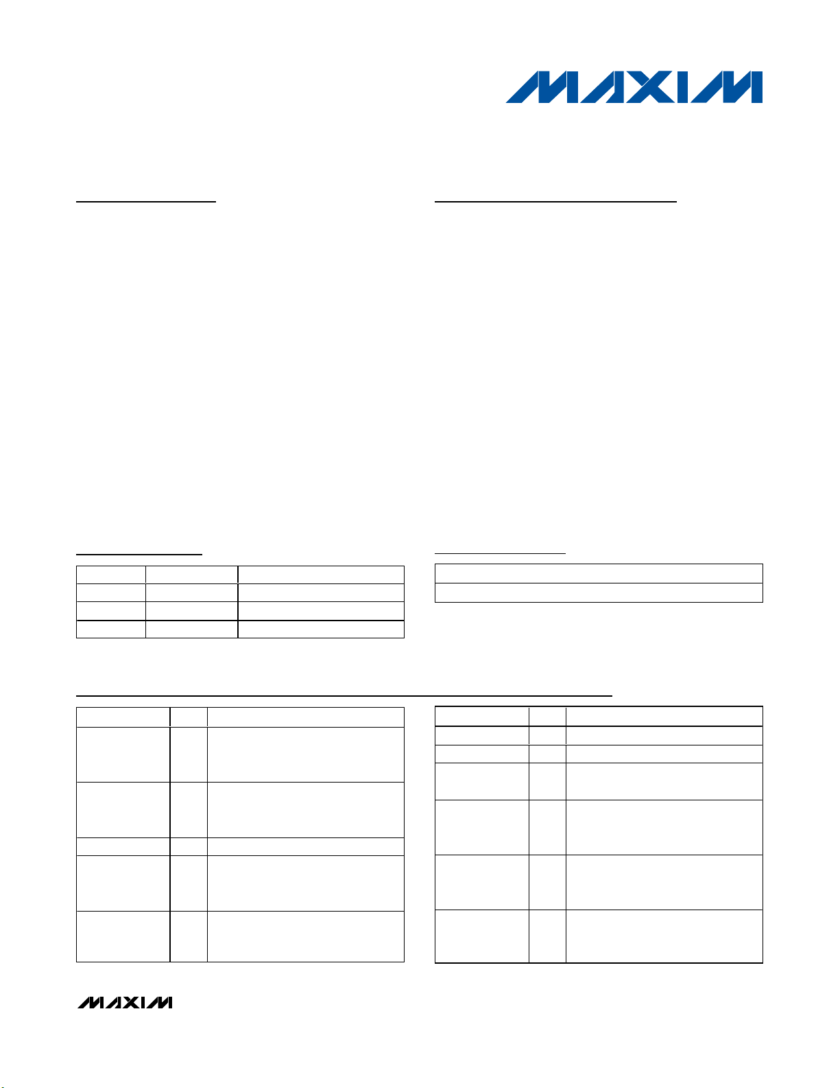
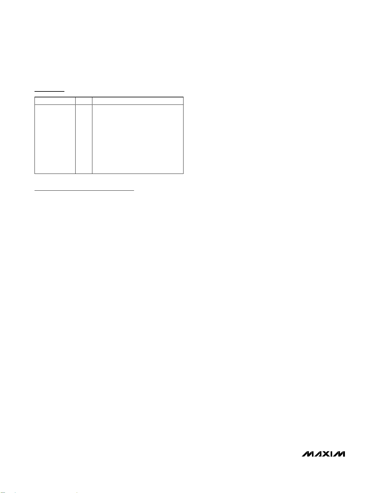
Figure 3. MAX2043 EV Kit PC Board Layout—Top Silkscreen Figure 4. MAX2043 EV Kit PC Board Layout—Top Soldermask
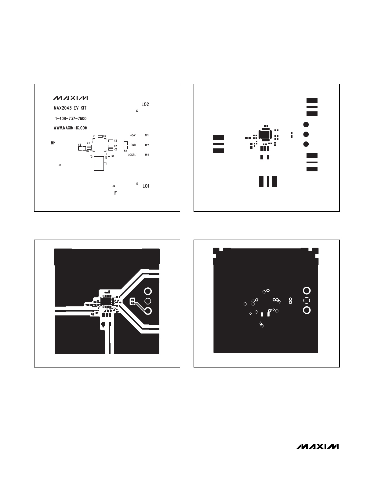
Figure 5. MAX2043 EV Kit PC Board Layout—Top Layer Metal Figure 6. MAX2043 EV Kit PC Board Layout—Inner Layer 2
(GND)
Page 7

Maxim cannot assume responsibility for use of any circuitry other than circuitry entirely embodied in a Maxim product. No circuit patent licenses are
implied. Maxim reserves the right to change the circuitry and specifications without notice at any time.
Maxim Integrated Products, 120 San Gabriel Drive, Sunnyvale, CA 94086 408-737-7600 _____________________
7
© 2006 Maxim Integrated Products Printed USA is a registered trademark of Maxim Integrated Products, Inc.
Evaluates: MAX2043
MAX2043 Evaluation Kit
Heaney
Figure 7. MAX2043 EV Kit PC Board Layout—Inner Layer 3
(Routes)
Figure 8. MAX2043 EV Kit PC Board Layout—Bottom Layer
Metal
Figure 9. MAX2043 EV Kit PC Board Layout—Bottom
Soldermask
Figure 10. MAX2043 EV Kit PC Board Layout—Bottom
Silkscreen
 Loading...