

Page 1
现货库存、技术资料、百科信息、热点资讯,精彩尽在鼎好!
General Description
The MAX2034 four-channel, low-power, ultra-low-noise
preamplifier is designed for ultrasound and medical
instrumentation applications. Each low-noise amplifier
has a single-ended input, differential output, a highly
accurate 19dB fixed gain, and a wide -3dB bandwidth
of 70MHz. The high-gain accuracy of the amplifier
allows for exceptional channel-to-channel gain matching, which is necessary for high-performance ultrasound-imaging applications. The MAX2034 also
includes an on-chip programmable input impedance
feature that allows the device to be compatible with a
variety of common source impedances ranging from
50Ω to 1kΩ. The input impedance of each amplifier
uses a feedback topology for active impedance matching. The active input impedance matching feature
achieves an exceptionally low 2.2dB noise figure with a
source and input impedance of 200Ω.
The MAX2034 has excellent dynamic and linearity performance characteristics optimized for all ultrasoundimaging modalities including second harmonic 2D
imaging and continuous wave Doppler. The device
achieves a second harmonic distortion of -68dBc at
V
OUT
= 1V
P-P
and fIN= 5MHz, and an ultrasound-specific* two-tone third-order intermodulation distortion performance of -55dBc at V
OUT
= 1V
P-P
and fIN= 5MHz.
The MAX2034 is also optimized for quick overload
recovery for operation under the large input signal conditions typically found in ultrasound input-buffer imaging applications.
The MAX2034 is available in a 48-pin thin QFN package with an exposed paddle. Electrical performance is
guaranteed over a 0°C to +70°C temperature range.
Features
♦ High-Level Integration of 4 Channels
♦ Digitally Programmable Input Impedance (RIN) of
50Ω, 100Ω, 200Ω, and 1kΩ
♦ Integrated Input Clamp
♦ Integrated Input-Damping Capacitor
♦ Ultra-Low 2.2dB Noise Figure at R
S
= RIN= 200Ω
♦ 70MHz, -3dB Bandwidth
♦ Low 58mW/Channel Power Dissipation
♦ HD2 of -68dBc at V
OUT
= 1V
P-P
and fIN= 5MHz for
Exceptional Second Harmonic Imaging
Performance
♦ Two-Tone Ultrasound-Specific* IMD3 of -55dBc at
V
OUT
= 1V
P-P
and fIN= 5MHz for Exceptional
PW/CW Doppler Performance
♦ Quick Large-Signal Overload Recovery
♦ Single +5V Supply Operation
♦ Sleep Mode
MAX2034
Quad-Channel, Ultra-Low-Noise Amplifier with
Digitally Programmable Input Impedance
________________________________________________________________ Maxim Integrated Products 1
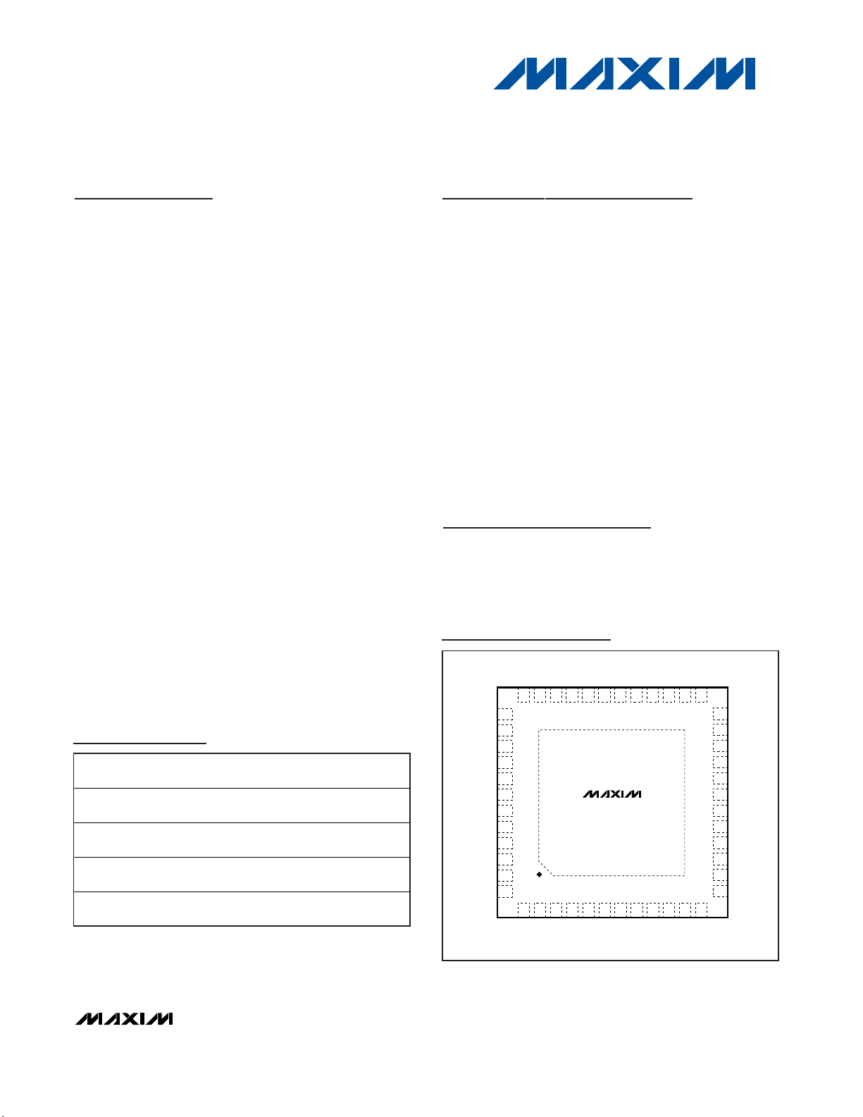
TOP VIEW
MAX2034
THIN QFN
13
14
15
16
17
18
19
20
21
22
23
24
INC4
INB4
GND
V
CC
V
CC
D1
D0
V
CC
GND
GND
OUT4-
OUT4+
48
47
46
45
44
43
42
41
40
39
38
37
1
2
345678910
11
12
IN1
ZF1
GND
V
CC
V
CC
PD
D2
V
CC
GND
GND
V
CC
GND
IN4
ZF4
INB3
INC3
IN3
ZF3
INB2
INC2
IN2
ZF2
INB1
INC1
36
35
34 33 32 31 30 29 28 27
26
25
GND
GND
VCCOUT3-
OUT3+
VCCOUT2-
OUT2+
GND
V
CC
OUT1-
OUT1+
Pin Configuration
19-3969; Rev 1; 3/07
For pricing, delivery, and ordering information, please contact Maxim/Dallas Direct! at
1-888-629-4642, or visit Maxim’s website at www.maxim-ic.com.
PART
TEMP
RANGE
PINPACKAGE
PKG
CODE
MAX2034CTM+
48 Thin QFN-EP**
(7mm x 7mm)
T4877-4
MAX2034CTM
48 Thin QFN-EP**
(7mm x 7mm)
T4877-4
MAX2034CTM+T
48 Thin QFN-EP**
(7mm x 7mm)
T4877-4
MAX2034CTM-T
48 Thin QFN-EP**
(7mm x 7mm)
T4877-4
Ordering Information
**EP = Exposed paddle.
+Denotes lead-free package.
T = Tape-and-reel package.
*See the Ultrasound-Specific IMD3 Specification in the
Applications Information section.
Typical Application Circuit appears at end of data sheet.
Applications
Ultrasound Imaging
Sonar Signal Amplification
0°C to +70°C
0°C to +70°C
0°C to +70°C
0°C to +70°C
Page 2
MAX2034
Quad-Channel, Ultra-Low-Noise Amplifier with
Digitally Programmable Input Impedance
2 _______________________________________________________________________________________
ABSOLUTE MAXIMUM RATINGS
DC ELECTRICAL CHARACTERISTICS
(MAX2034 Typical Application Circuit, VCC= +4.75V to +5.25V, no input signal applied between IN1–IN4 and GND, TA= 0°C to +70°C.
Typical values are at V
CC
= +5.0V and TA= +25°C, unless otherwise noted.) (Note 1)
Stresses beyond those listed under “Absolute Maximum Ratings” may cause permanent damage to the device. These are stress ratings only, and functional
operation of the device at these or any other conditions beyond those indicated in the operational sections of the specifications is not implied. Exposure to
absolute maximum rating conditions for extended periods may affect device reliability.
V
CC
to GND ...........................................................-0.3V to +5.5V
Any Other Pins to GND...............................-0.3V to (V
CC
+ 0.3V)
IN_ to INB_ ..................................................................-2V to +2V
INC_ to GND .....................................................-24mA to +24mA
Continuous Power Dissipation (T
A
= +70°C)
48-Pin TQFN (derated 40mW/°C above +70°C) ........3200mW
Operating Temperature Range...............................0°C to +70°C
Junction Temperature......................................................+150°C
θJC...................................................................................0.8°C/W
θ
JA
....................................................................................25°C/W
Storage Temperature Range .............................-40°C to +150°C
Lead Temperature (soldering, 10s) .................................+300°C
PARAMETER
CONDITIONS
UNITS
Supply Voltage V
CC
V
I
CC
Normal mode (PD = 0), no signals applied, see
the Typical Operating Characteristics for I
CC
as
a function of input signal
Total Supply Current
4
mA
LOGIC INPUTS (PD, D2, D1, D0)
Input High Voltage V
IH
V
Input Low Voltage V
IL
V
Input Current with Logic-High I
IH
1µA
Input Current with Logic-Low I
IL
1µA
AC ELECTRICAL CHARACTERISTICS
(MAX2034 Typical Application Circuit, VCC= +4.75V to +5.25V, source impedance RS= 200Ω, PD = 0, D2/D1/D0 = 0/1/0 (RIN= 200Ω),
signal AC-coupled to IN_, INB_ is AC grounded, V
OUT
is the differential output between OUT_+ and OUT_-, f
IN_
= 5MHz, RL= 200Ω
between the differential outputs, C
L
= 20pF from each output to ground, TA= 0°C to +70°C. Typical values are at VCC= 5.0V and TA=
+25°C, unless otherwise noted.) (Note 1)
PARAMETER
CONDITIONS
UNITS
D2/D1/D0 = 0/0/0 53
D2/D1/D0 = 0/0/1
D2/D1/D0 = 0/1/0
Input Resistance R
IN
D2/D1/D0 = 0/1/1
Ω
Typ i cal Inp ut Resi stance V ar i ati on
fr om N om i nal P r og r am m ed
%
Input Capacitance C
IN
40 pF
Gain A
V
(OUT_+ - OUT_-) / IN_ 19 dB
Part-to-Part Gain Variation from
Nominal
T
A
= +25oC, RL = 200Ω ±10% 0
dB
-3dB Small-Signal Gain
Bandwidth
f
-3dB
D2/D1/D0 = 0/0/0, (50Ω input impedance),
V
OUT
= 0.2V
P-P
70
MHz
Slew Rate
V/µs
SYMBOL
MIN TYP MAX
4.75 5.0 5.25
46.5 54.5
I
CC,PD
SYMBOL
Sleep mode (PD = 1), V
= 112mV
IN_
at 5MHz 0.8
P-P
4.0
MIN TYP MAX
105
206
870
±1
±0.1 ±0.5
280
1.0
Page 3
MAX2034
Quad-Channel, Ultra-Low-Noise Amplifier with
Digitally Programmable Input Impedance
_______________________________________________________________________________________ 3
AC ELECTRICAL CHARACTERISTICS (continued)
(MAX2034 Typical Application Circuit, VCC= +4.75V to +5.25V, source impedance RS= 200Ω, PD = 0, D2/D1/D0 = 0/1/0 (RIN= 200Ω),
signal AC-coupled to IN_, INB_ is AC grounded, V
OUT
is the differential output between OUT_+ and OUT_-, f
IN_
= 5MHz, RL= 200Ω
between the differential outputs, C
L
= 20pF from each output to ground, TA= 0°C to +70°C. Typical values are at VCC= 5.0V and TA=
+25°C, unless otherwise noted.) (Note 1)
PARAMETER
SYMBOL
CONDITIONS
MIN
TYP
MAX
UNITS
RS = RIN = 50Ω
RS = RIN = 100Ω
RS = RIN = 200Ω
Noise Figure NF
R
S
= RIN = 1000Ω
dB
Input-Referred Noise Voltage D2 = 1 (high input impedance), f
IN_
= 5MHz
nV/√Hz
Input-Referred Noise Current D2 = 1 (high input impedance), f
IN_
= 5MHz
pA/√Hz
f
IN_
= 5MHz, V
OUT
= 1V
P-P
differential
Second Harmonic HD2
f
IN_
= 10MHz, V
OUT
= 1V
P-P
differential
dBc
f
IN_
= 5MHz, V
OUT
= 1V
P-P
differential
Third Harmonic HD3
f
IN_
= 10MHz, V
OUT
= 1V
P-P
differential
dBc
4.99MHz tone relative to the second tone at
5.01MHz, which is 25dB lower than the first tone
at 5.00MHz, V
OUT
= 1V
P-P
differential
Two-Tone Intermodulation
Distortion (Note 2)
IMD3
7.49MHz tone relative to the second tone at
7.51MHz, which is 25dB lower than the first tone
at 7.50MHz, V
OUT
= 1V
P-P
differential
dBc
Maximum Output Signal
Amplitude
Differential output
V
P-P
Gain Compression
Gain at V
IN_
= 112mV
P-P
relative to gain at
V
IN_
= 550mV
P-P
3dB
Output Common-Mode Level
V
Output Impedance Single-ended
Ω
Phase Matching Between
Channels
Phase difference between channels with V
IN_
=
195mV peak (-3dB full scale), f
IN_
= 10MHz
deg
Channel-to-Channel Crosstalk
50 66 dB
Switch Time from Normal to Sleep
Mode
Supply current settles to 90% of nominal sleepmode current I
CC,PD
ms
Switch Time from Sleep to Normal
Mode
V
OUT
settles to 90% of final 1V
P-P
output
ms
Note 1: Min and max limits at TA= +25°C and +70°C are guaranteed by design, characterization, and/or production test.
Note 2: See the Ultrasound-Specific IMD3 Specification in the Applications Information section.
f
= 10MHz, V
IN_
= 1V
OUT
adjacent channels
P-P,
4.1
2.9
2.2
1.4
0.87
2.1
-50 -68
-66
-50
-44
-45 -55
-52
4.4
0.5
2.45
5.3
±1.5
0.3
0.3
Page 4
MAX2034
Quad-Channel, Ultra-Low-Noise Amplifier with
Digitally Programmable Input Impedance
4 _______________________________________________________________________________________
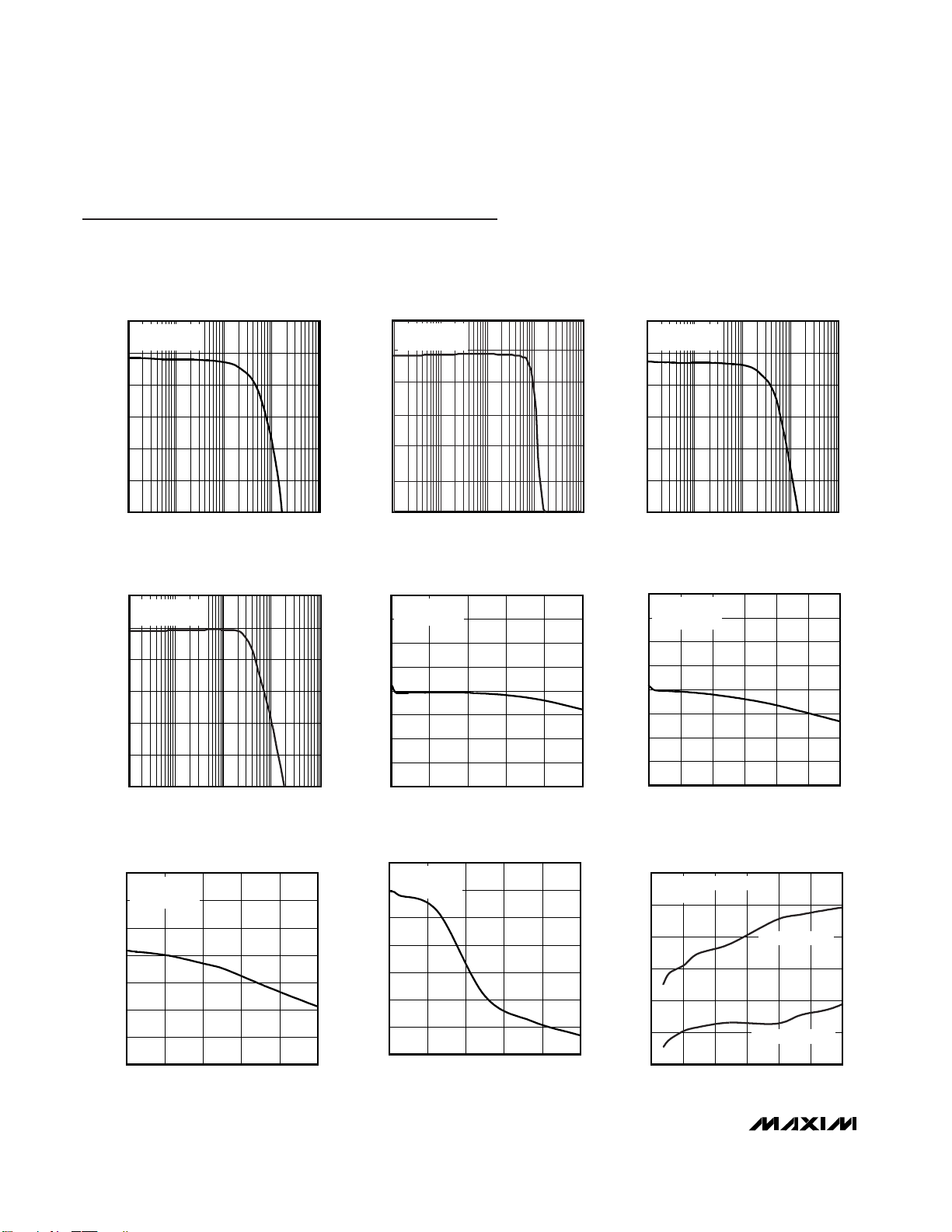
Typical Operating Characteristics
(MAX2034 Typical Application Circuit, VCC= +4.75V to +5.25V, source impedance RS= 200Ω, PD = 0, D2/D1/D0 = 0/1/0 (RIN= 200Ω),
signal AC-coupled to IN_, INB_ is AC grounded, V
OUT
is the differential output between OUT_+ and OUT_-, f
IN_
= 5MHz, RL= 200Ω
between the differential outputs, C
L
= 20pF from each output to ground, TA= 0°C to +70°C, unless otherwise specified.)
25
-5
0.1 10 1001 1000
SMALL-SIGNAL BANDWIDTH
vs. FREQUENCY
MAX2034 toc01
FREQUENCY (MHz)
GAIN (dB)
0
5
10
15
20
V
IN_
= 112mV
P-P
,
R
IN
= 200Ω
25
-5
0.1 10 1001 1000
SMALL-SIGNAL BANDWIDTH
vs. FREQUENCY
MAX2034 toc02
FREQUENCY (MHz)
GAIN (dB)
0
5
10
15
20
V
IN
= 112mV
P-P
R
IN
= 50Ω
25
-5
0.1 10 1001 1000
LARGE-SIGNAL BANDWIDTH
vs. FREQUENCY
MAX2034 toc03
FREQUENCY (MHz)
GAIN (dB)
0
5
10
15
20
V
IN_
= 500mV
P-P
,
RIN = 200Ω
25
-5
0.1 10 1001 1000
LARGE-SIGNAL BANDWIDTH
vs. FREQUENCY
MAX2034 toc04
FREQUENCY (MHz)
GAIN (dB)
0
5
10
15
20
V
IN
= 500mV
P-P
RIN = 50Ω
30
40
35
55
50
45
65
60
70
02010 30 40 50
COMPLEX INPUT IMPEDANCE MAGNITUDE
vs. FREQUENCY
MAX2034 toc05
FREQUENCY (MHz)
I
Z
IN
I
D2/D1/D0 = 0/0/0
R
IN
= 50Ω
60
80
70
110
100
90
130
120
140
010515202530
COMPLEX INPUT IMPEDANCE MAGNITUDE
vs. FREQUENCY
MAX2034 toc06
FREQUENCY (MHz)
I
Z
IN
I
D2/D1/D0 = 0/0/1
RIN = 100Ω
100
150
125
200
175
250
225
275
084121620
COMPLEX INPUT IMPEDANCE MAGNITUDE
vs. FREQUENCY
MAX2034 toc07
FREQUENCY (MHz)
I
Z
IN
I
D2/D1/D0 = 0/1/0
R
IN
= 200Ω
100
400
250
700
550
1000
850
1150
084121620
COMPLEX INPUT IMPEDANCE MAGNITUDE
vs. FREQUENCY
MAX2034 toc08
FREQUENCY (MHz)
I
Z
IN
I
D2/D1/D0 = 0/1/1
R
IN
= 1kΩ
-80
-60
-70
-40
-50
-30
-20
030
HARMONIC DISTORTION
vs. FREQUENCY
MAX2034 toc09
FREQUENCY (MHz)
HARMONIC DISTORTION (dBc)
105152520
V
OUT
= 1V
P-P
DIFFERENTIAL
RL = 200Ω
THIRD HARMONIC
SECOND HARMONIC
Page 5

MAX2034
Quad-Channel, Ultra-Low-Noise Amplifier with
Digitally Programmable Input Impedance
_______________________________________________________________________________________ 5
-70
-50
-60
-30
-40
-10
-20
0
0105152520 30
TWO-TONE ULTRASOUND-SPECIFIC IMD3
vs. FREQUENCY
MAX2034 toc10
FREQUENCY (MHz)
IMD3 (dBc)
V
OUT
= 1V
P-P
DIFFERENTIAL
RL = 200Ω
-30
-100
1 10 100
CHANNEL-TO-CHANNEL CROSSTALK
vs. FREQUENCY
-90
MAX2034 toc13
FREQUENCY (MHz)
CROSSTALK (dB)
-80
-70
-40
-50
-60
V
OUT
= 1V
P-P
DIFFERENTIAL
RL = 200Ω
ADJACENT CHANNELS
30
50
90
70
110
130
SUPPLY CURRENT
vs. DIFFERENTIAL OUTPUT VOLTAGE
MAX2034 toc14
DIFFERENTIAL OUTPUT VOLTAGE (V
P-P
)
SUPPLY CURRENT (mA)
02134
ALL CHANNELS ACTIVE
RL = 200Ω
NO LOAD
LARGE-SIGNAL RECOVERY
MAX2034 toc15
400ns/div
DIFFERENTIAL
OUTPUT
OUT_+ - OUT_-
2.0V/div
INPUT IN_
500mV/div
f
IN_
= 5MHz
Typical Operating Characteristics (continued)
(MAX2034 Typical Application Circuit, VCC= +4.75V to +5.25V, source impedance RS= 200Ω, PD = 0, D2/D1/D0 = 0/1/0 (RIN= 200Ω),
signal AC-coupled to IN_, INB_ is AC grounded, V
OUT
is the differential output between OUT_+ and OUT_-, f
IN_
= 5MHz, RL= 200Ω
between the differential outputs, C
L
= 20pF from each output to ground, TA= 0°C to +70°C, unless otherwise specified.)
GAIN-ERROR HISTOGRAM
50
SAMPLE SIZE = 243 UNITS
45
= 5MHz, VIN = 112mV
f
40
35
30
25
20
% OF UNITS
15
10
5
0
IN_
-0.20
-0.16
-0.12
P-P
0.02
-0.08
-0.04
GAIN ERROR (dB)
0.06
6
RIN = 200Ω
RL = 200Ω
5
f
IN_
4
3
2
VIN = 112mV
LARGE-SIGNAL NOISE FIGURE (dB)
1
0
0.1 100
MAX2034 toc12
0.10
0.14
0.18
LARGE-SIGNAL NOISE FIGURE
vs. OFFSET FREQUENCY
= 5MHz
VIN = 300mV
VIN = 200mV
P-P
OFFSET FREQUENCY (kHz)
P-P
P-P
SMALL-SIGNAL
NOISE FIGURE
101
MAX2034 toc11
Page 6

MAX2034
Quad-Channel, Ultra-Low-Noise Amplifier with
Digitally Programmable Input Impedance
6 _______________________________________________________________________________________
Typical Operating Characteristics (continued)
(MAX2034 Typical Application Circuit, VCC= +4.75V to +5.25V, source impedance RS= 200Ω, PD = 0, D2/D1/D0 = 0/1/0 (RIN= 200Ω),
signal AC-coupled to IN_, INB_ is AC grounded, V
OUT
is the differential output between OUT_+ and OUT_-, f
IN_
= 5MHz, RL= 200Ω
between the differential outputs, C
L
= 20pF from each output to ground, TA= 0°C to +70°C, unless otherwise specified.)
Pin Description
PIN NAME FUNCTION
1 INC1 Channel 1 Analog Input Clamp. Input port to the integrated clamping diodes.
2 INB1 Channel 1 Analog Bypass Input. Connect a capacitor to GND as close as possible to the pin.
3 ZF2 Channel 2 Active Impedance-Matching Port. AC-couple to the source circuit with a capacitor.
4 IN2
Channel 2 LNA Analog Input. Single-ended input for channel 2 amplifier. Connect the analog input to
the source circuit through a series capacitor.
5 INC2 Channel 2 Analog Input Clamp. Input port to the integrated clamping diodes.
6 INB2 Channel 2 Analog Bypass Input. Connect a capacitor to GND as close as possible to the pin.
7 ZF3 Channel 3 Active Impedance-Matching Port. AC-couple to the source circuit with a capacitor.
8 IN3
Channel 3 LNA Analog Input. Single-ended input for channel 3 amplifier. Connect the analog input to
the source circuit through a series capacitor.
9 INC3 Channel 3 Analog Input Clamp. Input port to the integrated clamping diodes.
10 INB3 Channel 3 Analog Bypass Input. Connect a capacitor to GND as close as possible to the pin.
11 ZF4 Channel 4 Active Impedance-Matching Port. AC-couple to the source circuit with a capacitor.
12 IN4
Channel 4 LNA Analog Input. Single-ended input for channel 4 amplifier. Connect the analog input to
the source circuit through a series capacitor.
13 INC4 Channel 4 Analog Input Clamp. Input port to the integrated clamping diodes.
14 INB4 Channel 4 Analog Bypass Input. Connect a capacitor to GND as close as possible to the pin.
15, 21, 22, 25,
26, 33, 37, 39,
40, 46
GND Ground
16, 17, 20, 27,
30, 34, 38, 41,
44, 45
V
CC
5V Power Supply. Supply for the four LNAs. Bypass each VCC supply with a 100nF capacitor as
close as possible to the pin.
LARGE-SIGNAL RECOVERY
MAX2034 toc16
f
= 10MHz
IN_
CLAMP SYMMETRY UNDER
TRANSMIT RECOVERY
f
IN_
MAX2034 toc17
= 5MHz
400ns/div
INPUT IN_
500mV/div
DIFFERENTIAL
OUTPUT
OUT_+ - OUT_-
2.0V/div
200ns/div
SINGLE-ENDED
OUTPUT OUT_+
1V/div
SINGLE-ENDED
OUTPUT OUT_1V/div
Page 7

Detailed Description
The MAX2034 is a four-channel, ultra-low-noise preamplifier. Each amplifier features single-ended inputs, differential outputs, and provides an accurate fixed gain of
19dB with a wide -3dB bandwidth of 70MHz. The highgain accuracy of the amplifier allows for exceptional
channel-to-channel gain matching, which is necessary
for high-performance ultrasound-imaging applications.
The device has an exceptionally low noise figure, making
it ideal for use in ultrasound front-end designs. Noise figure is typically 2.2dB for a source impedance and programmed input impedance of 200Ω.
The MAX2034 is optimized for excellent dynamic range
and linearity performance characteristics, making it ideal
for ultrasound-imaging modalities including second harmonic 2D imaging and continuous wave Doppler. The
device achieves an HD2 of -68dBc at V
OUT
= 1V
P-P
and
f
IN_
= 5MHz, and an ultrasound-specific two-tone IMD3
performance of -55dBc at V
OUT
= 1V
P-P
and f
IN_
=
5MHz. See the Ultrasound-Specific IMD3 Specification in
the Applications Information section.
Active Impedance Matching
To provide exceptional noise-figure characteristics, the
input impedance of each amplifier uses a feedback
topology for active impedance matching. A feedback
resistor of the value (1 + (A / 2)) x RSis added between
the inverting output of the amplifier to the input. The
input impedance is the feedback resistor, ZF, divided
by 1 + (A / 2). The factor of two is due to the gain of the
amplifier, A, being defined with a differential output. For
common input impedances, the internal digitally programmed impedances can be used (see Table 1). For
other input impedances, program the impedance for
external resistor operation, and then use an externally
supplied resistor to set the input impedance according
to the above formula.
The gain and input impedance of the MAX2034 vs. frequency are shown in the Typical Operating Char-
acteristics. Both gain and input impedance are well
behaved, with no peaking characteristics. This allows
the device to be used with a variety of input networks,
with no requirement for series ferrite beads or shunt
capacitors for stability control.
MAX2034
Quad-Channel, Ultra-Low-Noise Amplifier with
Digitally Programmable Input Impedance
_______________________________________________________________________________________ 7
Pin Description (continued)
PIN NAME FUNCTION
18, 19, 42
Digitally Programmable Inputs. Programs the input impedance of each amplifier. See Table 1 on
input impedance programming information.
23 OUT4- Channel 4 LNA Analog Inverting Output
24 OUT4+ Channel 4 LNA Analog Noninverting Output
28 OUT3- Channel 3 LNA Analog Inverting Output
29 OUT3+ Channel 3 LNA Analog Noninverting Output
31 OUT2- Channel 2 LNA Analog Inverting Output
32 OUT2+ Channel 2 LNA Analog Noninverting Output
35 OUT1- Channel 1 LNA Analog Inverting Output
36 OUT1+ Channel 1 LNA Analog Noninverting Output
43 PD Power-Down. Drive PD high to put the device in sleep mode. Drive PD low for normal mode.
47 ZF1 Channel 1 Active Impedance-Matching Port. AC-couple to the source circuit with a capacitor.
48 IN1
Channel 1 LNA Analog Input. Single-ended input for channel 1 amplifier. Connect the analog input to
the source circuit through a series capacitor.
EP GND Exposed Paddle. Solder the exposed paddle to the ground plane using multiple vias.
Table 1. Digitally Programmable Input
Impedance
D1, D0, D2
D2 D1 D0 RIN (Ω)
000 50
001 100
010 200
011 1k
100
101
110
111
Defined by external resistor
Page 8

MAX2034
Digitally Programmable Input Impedance
The MAX2034 features an on-chip digitally programmable input impedance, which makes the part compatible
with a variety of source impedances ranging from 50Ω
to 1kΩ. The input impedance can be programmed for
50Ω, 100Ω, 200Ω, or 1kΩ through the digital inputs D2,
D1, and D0. See Table 1 for programming details. In
addition to these fixed values, virtually any other input
impedance can be supported by using an off-chip
external feedback resistor, RF. To utilize this feature, set
D2, D1, and D0 to any of the four external resistor-controlled states shown in Table 1. The value of the off-chip
feedback resistor can be determined by using the following relationship:
RF= (1 + (A / 2)) x R
S
where RSis the source impedance, and A is the gain of
the amplifier (A = 9) defined with a differential output.
Noise Figure
The MAX2034 is designed to provide maximum input
sensitivity with its exceptionally low noise figure. The
input active devices are selected for very low equivalent input noise voltage and current, and they have
been optimized for source impedances from 50Ω to
1000Ω. Additionally, the noise contribution of the
matching resistor is effectively divided by 1 + (A / 2).
Using this scheme, typical noise figure of the amplifier
is approximately 2.2dB for RIN= RS= 200Ω. Table 2
illustrates the noise figure for other input impedances.
Input Clamp
The MAX2034 includes configurable integrated inputclamping diodes. The diodes are clamped to ground at
±275mV. The input-clamping diodes can be used to
prevent large transmit signals from overdriving the inputs
of the amplifiers. Overdriving the inputs could possibly
place charge on the input-coupling capacitor, causing
longer transmit overload recovery times. Input signals
are AC-coupled to the single-ended inputs IN1–IN4, but
are clamped with the INC1–INC4 inputs. See the Typical
Application Circuit. If external clamping devices are preferred, simply leave INC1–INC4 unconnected.
Quad-Channel, Ultra-Low-Noise Amplifier with
Digitally Programmable Input Impedance
8 _______________________________________________________________________________________
Functional Diagram
D2/D1/D0
ZF1
PD
IN1
INC1
INB1
OUT1-
OUT1+
ZF2
IN2
INC2
INB2
OUT2-
OUT2+
ZF3
IN3
INC3
INB3
OUT3-
OUT3+
ZF4
IN4
INC4
INB4
OUT4-
OUT4+
MAX2034
Table 2. Noise Figure vs. Source and
Input Impedances
Rs (Ω)R
IN
(Ω) NF (dB)
50 50 4.1
100 100 2.9
200 200 2.2
1000 1000 1.4
Page 9

Integrated Input Damping Capacitor
At high frequencies, gain peaking can occur due to an
active input termination becoming less effective when
the gain rolls off. Although an external shunting capacitor can be used to mitigate this effect, different input
impedance modes require different capacitor values.
The MAX2034 integrates a damping capacitor for each
of the four programmed input impedance modes. When
the input impedance is programmed by applying the
appropriate D2/D1/D0, an optimal capacitor value is
also chosen for the particular input impedance mode,
eliminating the need for external capacitors.
Overload Recovery
The device is also optimized for quick overload recovery for operation under the large input signal conditions
that are typically found in ultrasound input-buffer imaging applications. Internal signal clipping is symmetrical.
Input overloads can be prevented with the input-clamping diodes. See the Typical Operating Characteristics
that illustrate the rapid recovery time from a transmitrelated overload.
Sleep Mode
The sleep mode function allows the MAX2034 to be
configured in a low-power state when the amplifiers are
not being used. In sleep mode, all amplifiers are powered down, the total supply current of the device
reduces to 0.8mA, and the input impedance of each
amplifier is set at high impedance. Drive the PD input
high to activate sleep mode. For normal operation,
drive the PD input low.
Applications Information
Analog Input Coupling
AC-couple to ground the analog bypass input by connecting a 0.1µF capacitor at the INB1–INB4 input to
GND (0.1µF recommended). Since the amplifiers are
designed with a differential input stage, bypassing the
INB1–INB4 inputs configures the MAX2034 for singleended inputs at IN1–IN4.
Connect the IN1–IN4 inputs to their source circuits
through 0.1µF series capacitors. Connect the feedback
ports ZF1–ZF4 to the source circuits through 0.018µF
capacitors. (These capacitors will be 1/(5.5) as large as
the input-coupling capacitors. This equalizes the highpass filter characteristic of both the input and feedback
input ports, due to the feedback resistance related by a
factor of 1/(5.5) to the input impedance.)
Note that the active input circuitry of the MAX2034 is
stable, and does not require external ferrite beads or
shunt capacitors to achieve high-frequency stability.
The Typical Application Circuit illustrates these cou-
pling capacitors. If a ground-referenced current-limiting
stage precedes the MAX2034 inputs, its output can be
connected to the integrated clamping diodes on pins
INC1–INC4 to facilitate very rapid recovery from transient overloads associated with transmitter operation in
ultrasound applications.
Analog Output Coupling
The differential outputs of the MAX2034 are capable of
driving a differential load impedance of 200Ω or
greater. The differential output has a common-mode
bias of approximately 2.45V. AC-couple these differential outputs if the next stage has a different commonmode input range.
Board Layout
The pin configuration of the MAX2034 is optimized to
facilitate a very compact physical layout of the device
and its associated discrete components. A typical
application for this device might incorporate several
devices in close proximity to handle multiple channels
of signal processing.
The exposed paddle (EP) of the MAX2034’s thin QFNEP package provides a low thermal-resistance path to
the die. It is important that the PC board on which the
MAX2034 is mounted be designed to conduct heat
from the EP. In addition, provide the EP with a lowinductance path to electrical ground. The EP MUST be
soldered to a ground plane on the PC board, either
directly or through an array of plated via holes.
MAX2034
Quad-Channel, Ultra-Low-Noise Amplifier with
Digitally Programmable Input Impedance
_______________________________________________________________________________________ 9
ULTRASOUND IMD3
-25dB
F1 - (F2 - F1) F1 F2 F2 + (F2 - F1)
Figure 1. Ultrasound IMD3 Measurement Technique
Page 10

MAX2034
Quad-Channel, Ultra-Low-Noise Amplifier with
Digitally Programmable Input Impedance
10 ______________________________________________________________________________________
D2/D1/D0
PD
ZF_
INC_
INB_
IN_
18nF
100nF
100nF
OUT_-
OUT_+
100nF
100nF
MAX2034
ONE CHANNEL
+V
-V
Figure 2. Typical Single-Channel Ultrasound Application Circuit
Ultrasound-Specific IMD3 Specification
Unlike typical communications specs, the two input
tones are not equal in magnitude for the ultrasoundspecific IMD3 two-tone specification. In this measurement, F1 represents reflections from tissue and F2
represents reflections from blood. The latter reflections
are typically 25dB lower in magnitude, and hence the
measurement is defined with one input tone 25dB lower
than the other. The IMD3 product of interest (F1 - (F2 F1)) presents itself as an undesired Doppler error signal in ultrasound applications. See Figure 1.
Page 11

MAX2034
Quad-Channel, Ultra-Low-Noise Amplifier with
Digitally Programmable Input Impedance
______________________________________________________________________________________ 11
Typical 200Ω Application Circuit
MAX2034
25
26
27
28
29
30
31
32
33
34
35
36
12
11
10
9
8
7
6
5
4
3
2
1
13
14
15 16 17
18 19 20 21 22
23
24
48
47
46 45 44
43 42 41 40 39
38
37
GND
INC1
INB1
ZF2
INB2
ZF3
IN3
INC4
INB4
GND
V
CC
V
CC
V
CC
D1
D0
OUT3+
OUT2-
OUT2+
GND
OUT1-
V
CC
D2
PD
V
CC
V
CC
GND
ZF1
OUT1+
IN1
INC3
INB3
ZF4
IN4
GND
GND
OUT4-
OUT4+
OUT3-
GND
GND
GND
VCCGND
IN2
INC2
+5V
+5V
+5V
R
S
= 200Ω
100nF
100nF
100nF
100nF
100nF
100nF
100nF
100nF
100nF
100nF
18nF
18nF
18nF
100nF
18nF
100nF
100nF
100nF
100nF
100nF
100nF
R
S
= 200Ω
RS = 200Ω
R
S
= 200Ω
100nF
100nF
100nF
100nF
100nF
100nF
V
CC
V
CC
V
CC
EXPOSED PADDLE
Page 12

MAX2034
Quad-Channel, Ultra-Low-Noise Amplifier with
Digitally Programmable Input Impedance
12 ______________________________________________________________________________________
Package Information
(The package drawing(s) in this data sheet may not reflect the most current specifications. For the latest package outline information,
go to www.maxim-ic.com/packages
.)
32, 44, 48L QFN.EPS
e
L
e
L
A1AA2
E/
2
E
D/2
D
DETAIL
A
D2/2
D2
b
L
k
E2/2
E2
(NE-1) X
e
(ND-1) X
e
e
C
L
C
L
C
L
C
L
k
DETAIL
B
e
L
L1
PACKAGE OUTLINE
21-0144
2
1
E
32, 44, 48, 56L THIN QFN, 7x7x0.8mm
Page 13

MAX2034
Quad-Channel, Ultra-Low-Noise Amplifier with
Digitally Programmable Input Impedance
Maxim cannot assume responsibility for use of any circuitry other than circuitry entirely embodied in a Maxim product. No circuit patent licenses are
implied. Maxim reserves the right to change the circuitry and specifications without notice at any time.
Maxim Integrated Products, 120 San Gabriel Drive, Sunnyvale, CA 94086 408-737-7600 ____________________ 13
© 2007 Maxim Integrated Products is a registered trademark of Maxim Integrated Products, Inc.
Package Information
(The package drawing(s) in this data sheet may not reflect the most current specifications. For the latest package outline information,
go to www.maxim-ic.com/packages
.)
PACKAGE OUTLINE
21-0144
2
2
E
32, 44, 48, 56L THIN QFN, 7x7x0.8mm
Springer
Revision History
Pages changed at Rev 1: 1, 3, 4, 11, 12
 Loading...