

Page 1
General Description
The MAX2032 high-linearity passive upconverter or
downconverter mixer is designed to provide +33dBm
IIP3, 7dB NF, and 7dB conversion loss for a 650MHz to
1000MHz RF frequency range to support a multitude of
base-station applications. With a 650MHz to 1250MHz
LO frequency range, this particular mixer is ideal for
high-side LO injection architectures. For a pin-to-pincompatible mixer meant for low-side LO injection, refer
to the MAX2029.
In addition to offering excellent linearity and noise performance, the MAX2032 also yields a high level of component integration. This device includes a doublebalanced passive mixer core, a dual-input LO selectable switch, and an LO buffer. On-chip baluns are also
integrated to allow for a single-ended RF input for
downconversion (or RF output for upconversion) and
single-ended LO inputs. The MAX2032 requires a nominal LO drive of 0dBm, and supply current is guaranteed
to be below 100mA.
The MAX2032 is pin compatible with the MAX2039/
MAX2041 1700MHz to 2200MHz mixers, making this
family of passive upconverters and downconverters
ideal for applications where a common PCB layout is
used for both frequency bands.
The MAX2032 is available in a compact 20-pin thin
QFN package (5mm x 5mm) with an exposed pad.
Electrical performance is guaranteed over the extended
-40°C to +85°C temperature range.
Applications
Features
♦ 650MHz to 1000MHz RF Frequency Range
♦ 650MHz to 1250MHz LO Frequency Range
♦ 570MHz to 900MHz LO Frequency Range
(Refer to the MAX2029 Data Sheet)
♦ DC to 250MHz IF Frequency Range
♦ 7dB Conversion Loss
♦ +33dBm Input IP3
♦ +24dBm Input 1dB Compression Point
♦ 7dB Noise Figure
♦ Integrated LO Buffer
♦ Integrated RF and LO Baluns
♦ Low -3dBm to +3dBm LO Drive
♦ Built-In SPDT LO Switch with 49dB LO1 to LO2
Isolation and 50ns Switching Time
♦ Pin Compatible with the MAX2039/MAX2041
1700MHz to 2200MHz Mixers
♦ External Current-Setting Resistor Provides Option
for Operating Mixer in Reduced-Power/ReducedPerformance Mode
MAX2032
High-Linearity, 650MHz to 1000MHz Upconversion/
Downconversion Mixer with LO Buffer/Switch
________________________________________________________________
Maxim Integrated Products
1
19-4965; Rev 0; 9/09
For pricing, delivery, and ordering information, please contact Maxim Direct at 1-888-629-4642,
or visit Maxim’s website at www.maxim-ic.com.
EVALUATION KIT
AVAILABLE
cdma2000 is a registered trademark of Telecommunications
Industry Association.
iDEN is a registered trademark of Motorola, Inc.
WiMAX is a trademark of WiMAX Forum.
WCDMA/LTE and
cdma2000®Base
Stations
GSM 850/GSM 900 2G
and 2.5G EDGE Base
Stations
Integrated Digital
Enhanced Network
(iDEN
®
) Base Stations
WiMAXTMBase Stations
and Customer Premise
Equipment
Predistortion Receivers
Microwave and Fixed
Broadband Wireless
Access
Wireless Local Loop
Digital and Spread-
Spectrum Communication
Systems
Ordering Information
+
Denotes a lead(Pb)-free/RoHS-compliant package.
T = Tape and reel.
*
EP = Exposed pad.
MAX2032
TOP VIEW
4
5
3
2
12
11
13
LOBIAS
LOSEL
GND
14
V
CC
IF+
GND
GND
GND
67
TAP
910
20 19 17 16
GND
GND
V
CC
GND
GND
LO1
V
CC
IF-
8
18
RF
+
1
15
LO2
V
CC
EP
Pin Configuration/
Functional Diagram
PART TEMP RANGE PIN-PACKAGE
M AX 2032E TP + - 40°C to + 85° C 20 Thi n QFN- E P *
M AX 2032E TP + T- 40°C to + 85° C 20 Thi n QFN- E P *
Page 2
MAX2032
High-Linearity, 650MHz to 1000MHz Upconversion/
Downconversion Mixer with LO Buffer/Switch
2 _______________________________________________________________________________________
ABSOLUTE MAXIMUM RATINGS
Stresses beyond those listed under “Absolute Maximum Ratings” may cause permanent damage to the device. These are stress ratings only, and functional
operation of the device at these or any other conditions beyond those indicated in the operational sections of the specifications is not implied. Exposure to
absolute maximum rating conditions for extended periods may affect device reliability.
VCCto GND...........................................................-0.3V to +5.5V
RF (RF is DC shorted to GND through a balun)..................50mA
LO1, LO2 to GND ..................................................-0.3V to +0.3V
IF+, IF- to GND ...........................................-0.3V to (V
CC
+ 0.3V)
TAP to GND ...........................................................-0.3V to +1.4V
LOSEL to GND ...........................................-0.3V to (V
CC
+ 0.3V)
LOBIAS to GND..........................................-0.3V to (V
CC
+ 0.3V)
RF, LO1, LO2 Input Power (Note 1) ...............................+20dBm
Continuous Power Dissipation (Note 2)....................................5W
θ
J
A
(Notes 3, 4)..............................................................+38°C/W
θ
J
C
(Notes 2, 3)..............................................................+13°C/W
Operating Temperature Range (Note 5) .....T
C
= -40°C to +85°C
Junction Temperature......................................................+150°C
Storage Temperature Range .............................-65°C to +150°C
Lead Temperature (soldering, 10s) .................................+300°C
DC ELECTRICAL CHARACTERISTICS
(
Typical Application Circuit
, VCC= 4.75V to 5.25V, no RF signals applied, TC= -40°C to +85°C. IF+ and IF- are DC grounded through an
IF balun. Typical values are at V
CC
= 5V, TC= +25°C, unless otherwise noted.)
RECOMMENDED AC OPERATING CONDITIONS
Note 1: Maximum, reliable, continuous input power applied to the RF and IF port of this device is +12dBm from a 50Ω source.
Note 2: Based on junction temperature T
J
= TC+ (θJCx VCCx ICC). This formula can be used when the temperature of the exposed
pad is known while the device is soldered down to a PCB. See the
Applications Information
section for details. The junction
temperature must not exceed +150°C.
Note 3: Package thermal resistances were obtained using the method described in JEDEC specification JESD51-7, using a four-
layer board. For detailed information on package thermal considerations, refer to www.maxim-ic.com/thermal-tutorial
.
Note 4: Junction temperature T
J
= TA+ (θJAx VCCx ICC). This formula can be used when the ambient temperature of the PCB is
known. The junction temperature must not exceed +150°C.
Note 5: T
C
is the temperature on the exposed pad of the package. TAis the ambient temperature of the device and PCB.
PARAMETER SYMBOL CONDITIONS MIN TYP MAX UNITS
Supply Voltage V
Supply Current I
LOSEL Input Logic-Low V
LOSEL Input Logic-High V
CC
CC
IL
IH
4.75 5.00 5.25 V
2V
85 100 mA
0.8 V
RF Frequency f
LO Frequency f
IF Frequency f
LO Drive Level P
PARAMETER SYMBOL CONDITIONS MIN TYP MAX UNITS
RF
LO
IF
LO
C om p onents tuned for the 700M H z b and
( Tab l e 1) , C 1 = 7p F, C 5 = 3.3p F ( N otes 6, 7)
C om p onents tuned for the 800M H z/900M H z
cel l ul ar b and ( Tab l e 1) , C 1 = 82p F,
C 5 = 2.0p F ( N ote 6)
(Notes 6, 7) 650 1250 MHz
IF frequency range depends on external IF
transformer selection
(Note 6) -3 +3 dBm
650 850
800 1000
0 250 MHz
MHz
Page 3
MAX2032
High-Linearity, 650MHz to 1000MHz Upconversion/
Downconversion Mixer with LO Buffer/Switch
_______________________________________________________________________________________ 3
AC ELECTRICAL CHARACTERISTICS (800MHz/900MHz CELLULAR BAND DOWNCONVERTER OPERATION)
(
Typical Application Circuit,
optimized for the 800MHz/900MHz cellular band (see Table 1), C1 = 82pF, C5 = 2pF, L1 and C4 not
used, V
CC
= 4.75V to 5.25V, RF and LO ports driven from 50Ω sources, PLO= -3dBm to +3dBm, PRF= 0dBm, fRF= 815MHz to
1000MHz, f
LO
= 960MHz to 1180MHz, fIF= 160MHz, fLO> fRF, TC= -40°C to +85°C, unless otherwise noted. Typical values are at
V
CC
= 5V, PRF= 0dBm, PLO= 0dBm, fRF= 910MHz, fLO= 1070MHz, fIF= 160MHz, TC= +25°C, unless otherwise noted.) (Note 8)
Conversion Loss L
Conversion Loss Flatness
Conversion Loss Variation Over
Temperature
Input 1dB Compression Point P
Input Third-Order Intercept Point IIP3
Input IP3 Variation Over
Temperature
2LO - 2RF Spurious Response at IF 2 x 2 65 dBc
3LO - 3RF Spurious Response at IF 3 x 3 75 dBc
Noise Figure NF Single sideband 7.0 dB
Noise Figure Under Blocking
(Note 11)
LO1-to-LO2 Isolation (Note 10)
Maximum LO Leakage at RF Port PLO = +3dBm -27 dBm
Maximum LO Leakage at IF Port PLO = +3dBm -35 dBm
LO Switching Time 50% of LOSEL to IF, settled within 2 degrees 50 ns
Minimum RF-to-IF Isolation 45 dB
RF Port Return Loss 17 dB
LO Port Return Loss
IF Port Return Loss LO driven at 0dBm, RF terminated into 50Ω 17 dB
PARAMETER SYMBOL CONDITIONS MIN TYP MAX UNITS
7.0 dB
±0.18 dB
dB
dB
dB
dB
28
dB
30
1dB
IIP3
C
Flatness over any one of three frequency
bands (f
f
RF
f
RF
f
RF
TC = +25°C to -40°C -0.3
T
C
(Note 9) 24 dBm
f
RF1
P
RF
P
LO
TC = +25°C to -40°C 0.3
T
C
P
BLOCKER
P
BLOCKER
LO2 selected, PLO = +3dBm, TC = +25°C 42 51
LO1 selected, P
LO1/LO2 port selected, LO2/LO1, RF, and IF
terminated into 50Ω
LO1/LO2 port unselected, LO2/LO1, RF, and
IF terminated into 50Ω
= 160MHz):
IF
= 827MHz to 849MHz
= 869MHz to 894MHz
= 880MHz to 915MHz
= +25°C to +85°C 0.2
= 910MHz, f
= 0dBm/tone, fLO = 1070MHz,
= 0dBm, TC = +25°C (Note 10)
= +25°C to +85°C -0.3
= +8dBm 18
= +12dBm 22
= 911MHz,
RF2
= +3dBm, TC = +25°C 42 49
LO
29 33 dBm
Page 4
MAX2032
High-Linearity, 650MHz to 1000MHz Upconversion/
Downconversion Mixer with LO Buffer/Switch
4 _______________________________________________________________________________________
AC ELECTRICAL CHARACTERISTICS (UPCONVERTER OPERATION)
(
Typical Application Circuit
, L1 = 4.7nH, C4 = 6pF, C1 = 82pF, C5 not used, VCC= 4.75V to 5.25V, RF and LO ports are driven from
50Ω sources, P
LO
= -3dBm to +3dBm, PIF= 0dBm, fRF= 815MHz to 1000MHz, fLO= 960MHz to 1180MHz, fIF= 160MHz, fLO> fRF,
T
C
= -40°C to +85°C, unless otherwise noted. Typical values are at VCC= 5V, PIF= 0dBm, PLO= 0dBm, fRF= 910MHz, fLO=
1070MHz, f
IF
= 160MHz, TC= +25°C, unless otherwise noted.) (Note 8)
Note 6: Operation outside this range is possible, but with degraded performance of some parameters.
Note 7: Not production tested.
Note 8: All limits include external component losses. Output measurements are taken at IF or RF port of the
Typical Application Circuit
.
Note 9: Compression point characterized. It is advisable not to continuously operate the mixer RF/IF inputs above +12dBm.
Note 10: Guaranteed by design.
Note 11: Measured with external LO source noise filtered, so its noise floor is -174dBm/Hz. This specification reflects the effects of all
SNR degradations in the mixer, including the LO noise as defined in Application Note 2021:
Specifications and Measurement
of Local Oscilator Noise in Integrated Circuit Base Station Mixers.
AC ELECTRICAL CHARACTERISTICS (700MHz BAND DOWNCONVERTER OPERATION)
(
Typical Application Circuit
, optimized for the 700MHz band (see Table 1), C1 = 7pF, C5 = 3.3pF, L1 and C4 are not used, VCC=
4.75V to 5.25V, RF and LO ports driven from 50Ω sources, P
LO
= -3dBm to +3dBm, PRF= 0dBm, fRF= 650MHz to 850MHz, fLO=
790MHz to 990MHz, f
IF
= 140MHz, fLO> fRF, TC= +25°C, unless otherwise noted. Typical values are at VCC= 5V, PRF= 0dBm,
P
LO
= 0dBm, fRF= 750MHz, fLO= 890MHz, fIF= 140MHz, TC= +25°C, unless otherwise noted.) (Notes 8, 10)
Conversion Loss L
Input 1dB Compression Point P
PARAMETER SYMBOL CONDITIONS MIN TYP MAX UNITS
Input Third-Order Intercept Point IIP3
LO Leakage at IF Port PLO = +3dBm -33 dBm
LO Leakage at RF Port PLO = +3dBm -20 dBm
RF-to-IF Isolation 36 49 dB
2LO - 2RF Spurious Response 2 x 2 65 dBc
3LO - 3RF Spurious Response 3 x 3 75 dBc
Conversion Loss L
Conversion Loss Flatness
Conversion Loss Variation Over
Temperature
Input 1dB Compression Point P
Input Third-Order Intercept Point IIP3
Input IP3 Variation Over
Temperature
LO ± 2IF Spur 64 dBc
LO ± 3IF Spur 83 dBc
Output Noise Floor P
PARAMETER SYMBOL CONDITIONS MIN TYP MAX UNITS
C
1dB
fRF = 750MHz, PRF = 0dBm, PLO = 0dBm 24 dBm
= 749MHz, f
f
RF1
f
= 890MHz, PRF = 0dBm/tone,
LO
= 0dBm
P
LO
C
Flatness over any one of three frequency
bands (f
f
= 827MHz to 849MHz
RF
= 869MHz to 894MHz
f
RF
f
= 880MHz to 915MHz
RF
TC = +25°C to -40°C -0.3
T
= +25°C to +85°C 0.4
C
(Note 9) 24 dBm
1dB
= 160MHz, f
f
IF1
= 0dBm/tone, fLO = 1070MHz,
P
IF
P
= 0dBm, TC = +25°C (Note 10)
LO
IIP3
TC = +25°C to -40°C 1.2
= +25°C to +85°C -0.9
T
C
OUT
6.1 6.9 8.1 dB
= 750MHz,
RF2
= 160MHz):
IF
= 161MHz,
IF2
= 0dBm (Note 11) -167 dBm/Hz
29 33 dBm
7.4 dB
±0.3 dB
28 31 dBm
dB
dB
Page 5
MAX2032
High-Linearity, 650MHz to 1000MHz Upconversion/
Downconversion Mixer with LO Buffer/Switch
_______________________________________________________________________________________
5
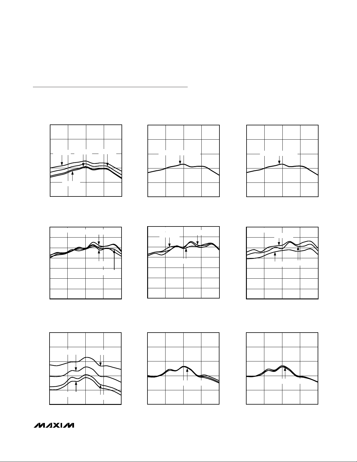
Typical Operating Characteristics
(
Typical Application Circuit
, optimized for the 800MHz/900MHz cellular band (see Table 1), C1 = 82pF, C5 = 2pF, L1 and C4 not used,
V
CC
= 5.0V, PLO= 0dBm, PRF= 0dBm, fLO> fRF, fIF= 160MHz, TC= +25°C, unless otherwise noted.)
Downconverter Curves
5
6
8
7
9
10
CONVERSION LOSS vs. RF FREQUENCY
MAX2032 toc01
RF FREQUENCY (MHz)
CONVERSION LOSS (dB)
800 900850 950 1000
TC = -40°C
TC = +25°C
TC = -25°C
TC = +85°C
5
6
8
7
9
10
CONVERSION LOSS vs. RF FREQUENCY
MAX2032 toc02
RF FREQUENCY (MHz)
CONVERSION LOSS (dB)
800 900850 950 1000
PLO = -3dBm, 0dBm, +3dBm
5
6
8
7
9
10
CONVERSION LOSS vs. RF FREQUENCY
MAX2032 toc03
RF FREQUENCY (MHz)
CONVERSION LOSS (dB)
800 900850 950 1000
VCC = 4.75V, 5.0V, 5.25V
INPUT IP3 vs. RF FREQUENCY
37
PRF = 0dBm/TONE
35
33
31
29
INPUT IP3 (dBm)
27
25
23
800 850 900 950 1000
NOISE FIGURE vs. RF FREQUENCY
10
9
8
7
NOISE FIGURE (dB)
6
5
800 900850 950 1000
TC = +85°C, +25°C
TC = -40°C
RF FREQUENCY (MHz)
TC = +25°C
TC = -40°C
RF FREQUENCY (MHz)
TC = +85°C
TC = -25°C
TC = -25°C
MAX2032 toc04
MAX2032 toc07
INPUT IP3 vs. RF FREQUENCY
37
PRF = 0dBm/TONE
35
33
31
29
INPUT IP3 (dBm)
27
25
23
PLO = +3dBm
800 850 900 950 1000
RF FREQUENCY (MHz)
PLO = 0dBm
PLO = -3dBm
NOISE FIGURE vs. RF FREQUENCY
10
9
8
7
NOISE FIGURE (dB)
6
5
800 900850 950 1000
PLO = -3dBm, 0dBm, +3dBm
RF FREQUENCY (MHz)
MAX2032 toc05
INPUT IP3 (dBm)
MAX2032 toc08
NOISE FIGURE (dB)
INPUT IP3 vs. RF FREQUENCY
37
PRF = 0dBm/TONE
35
33
31
29
27
25
23
800 850 900 950 1000
VCC = 5.25V
VCC = 4.75V
RF FREQUENCY (MHz)
VCC = 5.0V
NOISE FIGURE vs. RF FREQUENCY
10
9
8
7
6
5
800 900850 950 1000
VCC = 4.75V, 5.0V, 5.25V
RF FREQUENCY (MHz)
MAX2032 toc06
MAX2032 toc09
Page 6

MAX2032
High-Linearity, 650MHz to 1000MHz Upconversion/
Downconversion Mixer with LO Buffer/Switch
6 _______________________________________________________________________________________
Downconverter Curves
35
45
65
55
75
85
2LO - 2RF RESPONSE
vs. RF FREQUENCY
MAX2032 toc10
RF FREQUENCY (MHz)
2LO - 2RF RESPONSE (dBc)
800 900850 950 1000
TC = -40°C
TC = +85°C
TC = +25°C
TC = -25°C
PRF = 0dBm
35
45
65
55
75
85
2LO - 2RF RESPONSE
vs. RF FREQUENCY
MAX2032 toc11
RF FREQUENCY (MHz)
2LO - 2RF RESPONSE (dBc)
800 900850 950 1000
PLO = +3dBm
PLO = -3dBm
PLO = 0dBm
PRF = 0dBm
35
45
65
55
75
85
2LO - 2RF RESPONSE
vs. RF FREQUENCY
MAX2032 toc12
RF FREQUENCY (MHz)
2LO - 2RF RESPONSE (dBc)
800 900850 950 1000
PRF = 0dBm
VCC = 4.75V, 5.0V
VCC = 5.25V
Typical Operating Characteristics (continued)
(
Typical Application Circuit
, optimized for the 800MHz/900MHz cellular band (see Table 1), C1 = 82pF, C5 = 2pF, L1 and C4 not used,
V
CC
= 5.0V, PLO= 0dBm, PRF= 0dBm, fLO> fRF, fIF= 160MHz, TC= +25°C, unless otherwise noted.)
3LO - 3RF RESPONSE (dBc)
(dBm)
1dB
INPUT P
3LO - 3RF RESPONSE
vs. RF FREQUENCY
95
PRF = 0dBm
85
75
65
55
29
27
25
23
21
TC = +25°C
TC = +85°C
TC = -40°C, -25°C
800 900850 950 1000
RF FREQUENCY (MHz)
INPUT P
TC = +25°C
800 900850 950 1000
vs. RF FREQUENCY
1dB
TC = -25°C, +85°C
RF FREQUENCY (MHz)
TC = -40°C
95
MAX2032 toc13
85
75
65
3LO - 3RF RESPONSE (dBc)
55
800 900850 950 1000
29
MAX2032 toc16
27
(dBm)
1dB
25
INPUT P
23
21
800 900850 950 1000
3LO - 3RF RESPONSE
vs. RF FREQUENCY
PRF = 0dBm
PLO = 0dBm
RF FREQUENCY (MHz)
INPUT P
PLO = 0dBm, +3dBm
PLO = -3dBm
RF FREQUENCY (MHz)
PLO = -3dBm
PLO = +3dBm
vs. RF FREQUENCY
1dB
95
MAX2032 toc14
85
75
65
3LO - 3RF RESPONSE (dBc)
55
29
MAX2032 toc17
27
(dBm)
1dB
25
INPUT P
23
21
3LO - 3RF RESPONSE
vs. RF FREQUENCY
PRF = 0dBm
VCC = 5.25V
VCC = 5.0V
VCC = 4.75V
800 900850 950 1000
RF FREQUENCY (MHz)
INPUT P
800 900850 950 1000
vs. RF FREQUENCY
1dB
VCC = 5.25V
VCC = 4.75V
VCC = 5.0V
RF FREQUENCY (MHz)
MAX2032 toc15
MAX2032 toc18
Page 7

MAX2032
High-Linearity, 650MHz to 1000MHz Upconversion/
Downconversion Mixer with LO Buffer/Switch
_______________________________________________________________________________________
7
Downconverter Curves
Typical Operating Characteristics (continued)
(
Typical Application Circuit
, optimized for the 800MHz/900MHz cellular band (see Table 1), C1 = 82pF, C5 = 2pF, L1 and C4 not used,
V
CC
= 5.0V, PLO= 0dBm, PRF= 0dBm, fLO> fRF, fIF= 160MHz, TC= +25°C, unless otherwise noted.)
LO SWITCH ISOLATION
vs. LO FREQUENCY
60
LO SWITCH ISOLATION
vs. LO FREQUENCY
60
60
LO SWITCH ISOLATION
vs. LO FREQUENCY
55
50
TC = +85°C
45
LO SWITCH ISOLATION (dB)
40
850 1050950 1150 1250
TC = -40°C, -25°C
TC = +25°C
LO FREQUENCY (MHz)
LO LEAKAGE AT IF PORT
vs. LO FREQUENCY
-20
TC = -40°C, -25°C
-30
-40
-50
LO LEAKAGE AT IF PORT (dBm)
-60
960 10601010 1110 1160
TC = -40°C, -25°C
TC = +25°C
TC = +25°C
LO FREQUENCY (MHz)
TC = +85°C
TC = +85°C
LO LEAKAGE AT RF PORT
vs. LO FREQUENCY
-15
-20
-25
TC = -40°C, -25°C
MAX2032 toc19
55
50
45
LO SWITCH ISOLATION (dB)
40
850 1050950 1150 1250
-20
MAX2032 toc22
-30
-40
-50
LO LEAKAGE AT IF PORT (dBm)
-60
960 10601010 1110 1160
-15
-20
MAX2032 toc25
-25
PLO = -3dBm, 0dBm, +3dBm
LO FREQUENCY (MHz)
LO LEAKAGE AT IF PORT
vs. LO FREQUENCY
PLO = -3dBm, 0dBm, +3dBm
LO FREQUENCY (MHz)
LO LEAKAGE AT RF PORT
vs. LO FREQUENCY
MAX2032 toc20
55
50
45
LO SWITCH ISOLATION (dB)
40
850 1050950 1150 1250
-20
MAX2032 toc23
-30
-40
-50
LO LEAKAGE AT IF PORT (dBm)
-60
960 10601010 1110 1160
-15
-20
MAX2032 toc26
-25
VCC = 4.75V, 5.0V, 5.25V
LO FREQUENCY (MHz)
LO LEAKAGE AT IF PORT
vs. LO FREQUENCY
VCC = 5.25V
VCC = 4.75V
VCC = 5.0V
LO FREQUENCY (MHz)
LO LEAKAGE AT RF PORT
vs. LO FREQUENCY
VCC = 5.25V
MAX2032 toc21
MAX2032 toc24
MAX2032 toc27
-30
TC = +85°C
-35
LO LEAKAGE AT RF PORT (dBm)
-40
-45
850 1050950 1150 1250
LO FREQUENCY (MHz)
TC = +25°C
-30
PLO = -3dBm, 0dBm, +3dBm
-35
LO LEAKAGE AT RF PORT (dBm)
-40
-45
850 1050950 1150 1250
LO FREQUENCY (MHz)
-30
-35
LO LEAKAGE AT RF PORT (dBm)
-40
-45
850 1050950 1150 1250
VCC = 4.75V
LO FREQUENCY (MHz)
VCC = 5.0V
Page 8

MAX2032
High-Linearity, 650MHz to 1000MHz Upconversion/
Downconversion Mixer with LO Buffer/Switch
8 _______________________________________________________________________________________
Downconverter Curves
30
40
35
50
45
55
60
800 900850 950 1000
RF-TO-IF ISOLATION
vs. RF FREQUENCY
MAX2032 toc28
RF FREQUENCY (MHz)
RF-TO-IF ISOLATION (dB)
TC = -40°C, -25°C
TC = +85°C
TC = +25°C
30
40
35
50
45
55
60
800 900850 950 1000
RF-TO-IF ISOLATION
vs. RF FREQUENCY
MAX2032 toc29
RF FREQUENCY (MHz)
RF-TO-IF ISOLATION (dB)
PLO = -3dBm
PLO = 0dBm
PLO = +3dBm
30
40
35
50
45
55
60
800 900850 950 1000
RF-TO-IF ISOLATION
vs. RF FREQUENCY
MAX2032 toc30
RF FREQUENCY (MHz)
RF-TO-IF ISOLATION (dB)
VCC = 4.75V, 5.0V, 5.25V
Typical Operating Characteristics (continued)
(
Typical Application Circuit
, optimized for the 800MHz/900MHz cellular band (see Table 1), C1 = 82pF, C5 = 2pF, L1 and C4 not used,
V
CC
= 5.0V, PLO= 0dBm, PRF= 0dBm, fLO> fRF, fIF= 160MHz, TC= +25°C, unless otherwise noted.)
RF PORT RETURN LOSS
vs. RF FREQUENCY
0
5
10
15
20
RF PORT RETURN LOSS (dB)
PLO = -3dBm, 0dBm, +3dBm
25
30
750 850 900800 950 1000 1050
RF FREQUENCY (MHz)
LO SELECTED RETURN LOSS
vs. LO FREQUENCY
0
5
10
15
20
25
30
LO SELECTED RETURN LOSS (dB)
35
40
800 900 1000 1100 1200 1300
PLO = +3dBm
PLO = -3dBm
LO FREQUENCY (MHz)
PLO = 0dBm
0
INCLUDES IF TRANSFORMER
5
MAX2032 toc31
10
15
20
25
30
35
IF PORT RETURN LOSS (dB)
40
45
50
0200100 300 400 500
LO UNSELECTED RETURN LOSS
0
10
MAX2032 toc34
20
30
40
50
LO UNSELECTED RETURN LOSS (dB)
60
800 1300
IF PORT RETURN LOSS
vs. IF FREQUENCY
VCC = 4.75V, 5.0V, 5.25V
IF FREQUENCY (MHz)
vs. LO FREQUENCY
PLO = -3dBm, 0dBm, +3dBm
1000900 1100 1200
LO FREQUENCY (MHz)
0
5
MAX2032 toc32
MAX2032 toc35
10
15
20
25
30
35
IF PORT RETURN LOSS (dB)
40
45
50
100
90
80
SUPPLY CURRENT (mA)
70
60
IF PORT RETURN LOSS
vs. IF FREQUENCY
INCLUDES IF TRANSFORMER
PLO = -3dBm, 0dBm, +3dBm
0200100 300 400 500
IF FREQUENCY (MHz)
SUPPLY CURRENT
vs. TEMPERATURE (T
VCC = 5.25V
VCC = 4.75V
-40 10-15 35 60 85
TEMPERATURE (°C)
)
C
VCC = 5.0V
MAX2032 toc33
MAX2032 toc36
Page 9

MAX2032
High-Linearity, 650MHz to 1000MHz Upconversion/
Downconversion Mixer with LO Buffer/Switch
_______________________________________________________________________________________
9
Typical Operating Characteristics (continued)
(
Typical Application Circuit,
optimized for the 700MHz band (see Table 1), C1 = 7pF, C5 = 3.3pF, L1 and C4 are not used, VCC=
5V, P
LO
= 0dBm, PRF= 0dBm, fLO> fRF, fIF= 140MHz, TC= +25°C, unless otherwise noted.)
Downconverter Curves
CONVERSION LOSS vs. RF FREQUENCY
9
8
7
CONVERSION LOSS (dB)
6
TC = -40°C
5
650 850
RF FREQUENCY (MHz)
INPUT IP3 vs. RF FREQUENCY
36
P
= 0dBm/TONE
RF
34
TC = +25°C
32
30
INPUT IP3 (dBm)
TC = -40°C
28
CONVERSION LOSS vs. RF FREQUENCY
9
8
7
V
= 4.75V, 5.0V, 5.25V
CONVERSION LOSS (dB)
6
5
CC
650 850
RF FREQUENCY (MHz)
INPUT IP3 vs. RF FREQUENCY
36
PRF = 0dBm/TONE
34
V
= 5.25V
CC
32
30
INPUT IP3 (dBm)
28
VCC = 4.75V
VCC = 5.0V
800750700
TC = +85°C
TC = +25°C
TC = +25°C
800750700
TC = +85°C
9
MAX2032 toc37
8
7
CONVERSION LOSS (dB)
6
5
36
MAX2032 toc40
34
32
30
INPUT IP3 (dBm)
28
CONVERSION LOSS vs. RF FREQUENCY
P
= -3dBm, 0dBm, +3dBm
LO
650 850
RF FREQUENCY (MHz)
800750700
INPUT IP3 vs. RF FREQUENCY
PRF = 0dBm/TONE
PLO = -3dBm, 0dBm, +3dBm
MAX2032 toc38
MAX2032 toc41
MAX2032 toc39
MAX2032 toc42
26
650 850
RF FREQUENCY (MHz)
2LO - 2RF RESPONSE
vs. RF FREQUENCY
80
70
60
2LO - 2RF RESPONSE (dBc)
50
40
650 850
TC = +25°C
TC = -40°C
RF FREQUENCY (MHz)
800750700
PRF = 0dBm
TC = +85°C
800750700
26
650 850
80
MAX2032 toc43
70
60
2LO - 2RF RESPONSE (dBc)
50
40
650 850
RF FREQUENCY (MHz)
2LO - 2RF RESPONSE
vs. RF FREQUENCY
PLO = 0dBm
PLO = -3dBm
RF FREQUENCY (MHz)
800750700
PRF = 0dBm
PLO = +3dBm
800750700
26
650 850
80
MAX2032 toc44
70
60
2LO - 2RF RESPONSE (dBc)
50
40
650 850
RF FREQUENCY (MHz)
2LO - 2RF RESPONSE
vs. RF FREQUENCY
VCC = 4.75V, 5.0V, 5.25V
RF FREQUENCY (MHz)
800750700
P
RF
800750700
= 0dBm
MAX2032 toc45
Page 10

MAX2032
High-Linearity, 650MHz to 1000MHz Upconversion/
Downconversion Mixer with LO Buffer/Switch
10 ______________________________________________________________________________________
Typical Operating Characteristics (continued)
(
Typical Application Circuit,
optimized for the 700MHz band (see Table 1), C1 = 7pF, C5 = 3.3pF, L1 and C4 are not used, VCC=
5V, P
LO
= 0dBm, PRF= 0dBm, fLO> fRF, fIF= 140MHz, TC= +25°C, unless otherwise noted.)
Downconverter Curves
3LO - 3RF RESPONSE
vs. RF FREQUENCY
85
3LO - 3RF RESPONSE
vs. RF FREQUENCY
85
MAX2032 toc46
85
PRF = 0dBm
MAX2032 toc47
P
= 0dBmTC = +25°C
RF
3LO - 3RF RESPONSE
vs. RF FREQUENCY
VCC = 5.25V
PRF = 0dBm
75
65
3LO - 3RF RESPONSE (dBc)
TC = -40°C
TC = +85°C
75
P
= -3dBm, 0dBm, +3dBm
65
3LO - 3RF RESPONSE (dBc)
LO
75
65
3LO - 3RF RESPONSE (dBc)
VCC = 4.75V
VCC = 5.0V
MAX2032 toc48
55
650
RF FREQUENCY (MHz)
INPUT P
25
24
TC = +25°C
23
(dBm)
1dB
22
INPUT P
21
20
650 850
vs. RF FREQUENCY
1dB
TC = -40°C
RF FREQUENCY (MHz)
LO LEAKAGE AT IF PORT
vs. LO FREQUENCY
-15
T
= -40°C
C
-25
800750700
TC = +85°C
800750700
850
MAX2032 toc49
MAX2032 toc52
55
650
RF FREQUENCY (MHz)
INPUT P
25
24
23
(dBm)
1dB
22
INPUT P
21
PLO = -3dBm
20
650 850
vs. RF FREQUENCY
1dB
PLO = +3dBm
P
= 0dBm
LO
RF FREQUENCY (MHz)
LO LEAKAGE AT IF PORT
vs. LO FREQUENCY
-15
-25
PLO = +3dBm
55
800750700
800750700
850
MAX2032 toc50
650
RF FREQUENCY (MHz)
INPUT P
25
24
23
(dBm)
1dB
22
INPUT P
21
20
650 850
vs. RF FREQUENCY
1dB
VCC = 5.0V
VCC = 4.75V
RF FREQUENCY (MHz)
V
= 5.25V
CC
800750700
800750700
850
MAX2032 toc51
LO LEAKAGE AT IF PORT
vs. LO FREQUENCY
-15
MAX2032 toc53
-25
V
CC
= 5.25V
MAX2032 toc54
-35
TC = +25°C
LO LEAKAGE AT IF PORT (dBm)
-45
790
TC = +85°C
LO FREQUENCY (MHz)
-35
LO LEAKAGE AT IF PORT (dBm)
-45
940890840
990
790
PLO = 0dBm
LO FREQUENCY (MHz)
PLO = -3dBm
940890840
990
-35
LO LEAKAGE AT IF PORT (dBm)
-45
790
VCC = 4.75V
LO FREQUENCY (MHz)
VCC = 5.0V
940890840
990
Page 11

MAX2032
High-Linearity, 650MHz to 1000MHz Upconversion/
Downconversion Mixer with LO Buffer/Switch
______________________________________________________________________________________
11
Typical Operating Characteristics (continued)
(
Typical Application Circuit,
optimized for the 700MHz band (see Table 1), C1 = 7pF, C5 = 3.3pF, L1 and C4 are not used, VCC=
5V, P
LO
= 0dBm, PRF= 0dBm, fLO> fRF, fIF= 140MHz, TC= +25°C, unless otherwise noted.)
Downconverter Curves
LO LEAKAGE AT RF PORT
vs. LO FREQUENCY
-10
-15
-20
-25
LO LEAKAGE AT RF PORT (dBm)
-30
790 990
TC = -40°C
TC = +25°C
LO FREQUENCY (MHz)
2LO LEAKAGE AT RF PORT
vs. LO FREQUENCY
-20
TC = -40°C
-25
TC = +85°C
940890840
-10
MAX2032 toc55
-15
-20
-25
LO LEAKAGE AT RF PORT (dBm)
-30
-20
MAX2032 toc58
-25
LO LEAKAGE AT RF PORT
vs. LO FREQUENCY
P
= +3dBm
LO
PLO = -3dBm
PLO = 0dBm
790 990
LO FREQUENCY (MHz)
940890840
2LO LEAKAGE AT RF PORT
vs. LO FREQUENCY
PLO = +3dBm
-10
MAX2032 toc56
-15
-20
-25
LO LEAKAGE AT RF PORT (dBm)
-30
790 990
-20
MAX2032 toc59
-25
LO LEAKAGE AT RF PORT
vs. LO FREQUENCY
V
= 5.25V
CC
VCC = 5.0V
LO FREQUENCY (MHz)
VCC = 4.75V
940890840
2LO LEAKAGE AT RF PORT
vs. LO FREQUENCY
VCC = 5.25V
VCC = 5.0V
MAX2032 toc57
MAX2032 toc60
-30
TC = +25°C
-35
2LO LEAKAGE AT RF PORT (dBm)
-40
790 990
T
= +85°C
C
LO FREQENCY (MHz)
RF-TO-IF ISOLATION vs. RF FREQUENCY
60
TC = +85°C
50
40
RF-TO-IF ISOLATION (dB)
30
650 850
TC = -40°C
RF FREQUENCY (MHz)
TC = +25°C
-30
-35
2LO LEAKAGE AT RF PORT (dBm)
-40
940890840
790 990
PLO = -3dBm
LO FREQUENCY (MHz)
PLO = 0dBm
940890840
RF-TO-IF ISOLATION vs. RF FREQUENCY
60
MAX2032 toc61
50
P
= -3dBm, 0dBm, +3dBm
LO
40
RF-TO-IF ISOLATION (dB)
800750700
30
650
RF FREQUENCY (MHz)
800750700
850
-30
-35
2LO LEAKAGE AT RF PORT (dBm)
-40
790 990
RF-TO-IF ISOLATION vs. RF FREQUENCY
60
MAX2032 toc62
50
40
RF-TO-IF ISOLATION (dB)
30
650 850
LO FREQUENCY (MHz)
V
= 4.75V, 5.0V, 5.25V
CC
RF FREQUENCY (MHz)
VCC = 4.75V
940890840
MAX2032 toc63
800750700
Page 12

MAX2032
High-Linearity, 650MHz to 1000MHz Upconversion/
Downconversion Mixer with LO Buffer/Switch
12 ______________________________________________________________________________________
Typical Operating Characteristics (continued)
(
Typical Application Circuit,
optimized for the 700MHz band (see Table 1), C1 = 7pF, C5 = 3.3pF, L1 and C4 are not used, VCC=
5V, P
LO
= 0dBm, PRF= 0dBm, fLO> fRF, fIF= 140MHz, TC= +25°C, unless otherwise noted.)
Downconverter Curves
RF PORT RETURN LOSS
vs. RF FREQUENCY
0
5
10
15
RF PORT RETURN LOSS (dB)
20
25
500 1000
PLO = -3dBm, 0dBm, +3dBm
RF FREQUENCY (MHz)
900800700600
LO UNSELECTED RETURN LOSS
vs. LO FREQUENCY
0
10
IF PORT RETURN LOSS
vs. IF FREQUENCY
0
MAX2032 toc64
5
10
15
IF PORT RETURN LOSS (dB)
20
25
50 350
VCC = 4.75V, 5.0V, 5.25V
IF FREQUENCY (MHz)
100
MAX2032 toc67
90
fLO = 890MHz
MAX2032 toc65
300250200150100
SUPPLY CURRENT
vs. TEMPERATURE (T
= 5.25V
V
CC
LO SELECTED RETURN LOSS (dB)
LO SELECTED RETURN LOSS
vs. LO FREQUENCY
0
10
20
30
40
600 1200
C
PLO = 0dBm
PLO = +3dBm
PLO = -3dBm
1050900750
LO FREQUENCY (MHz)
)
MAX2032 toc68
MAX2032 toc66
P
20
30
LO UNSELECTED RETURN LOSS (dB)
40
= -3dBm, 0dBm, +3dBm
LO
600 1200
LO FREQENCY (MHz)
1050900750
80
SUPPLY CURRENT (mA)
70
60
-40 85
= 4.75V
V
CC
TEMPERATURE (NC)
= 5.0V
V
CC
603510-15
Page 13

MAX2032
High-Linearity, 650MHz to 1000MHz Upconversion/
Downconversion Mixer with LO Buffer/Switch
______________________________________________________________________________________
13
Typical Operating Characteristics (continued)
(
Typical Application Circuit
, L1 = 4.7nH, C4 = 6pF, C5 not used, VCC= 5.0V, PLO= 0dBm, PIF= 0dBm, fRF= f
LO
+ fIF, fIF= 160MHz,
T
C
= +25°C, unless otherwise noted.)
Upconverter Curves
CONVERSION LOSS vs. RF FREQUENCY
(L-C BPF TUNED FOR 810MHz RF FREQUENCY)
9
TC = +85°C
8
7
6
CONVERSION LOSS (dB)
TC = -40°C
5
TC = +25°C
TC = -25°C
CONVERSION LOSS vs. RF FREQUENCY
(L-C BPF TUNED FOR 810MHz RF FREQUENCY)
9
8
MAX2032 toc69
7
6
5
CONVERSION LOSS (dB)
4
PLO = -3dBm, 0dBm, +3dBm
MAX2032 toc70
CONVERSION LOSS vs. RF FREQUENCY
(L-C BPF TUNED FOR 810MHz RF FREQUENCY)
9
8
7
6
5
CONVERSION LOSS (dB)
4
VCC = 4.75V, 5.0V, 5.25V
MAX2032 toc71
4
750 850800 900 950 1000 1050
RF FREQUENCY (MHz)
INPUT IP3 vs. RF FREQUENCY
(L-C BPF TUNED FOR 810MHz RF FREQUENCY)
35
PIF = 0dBm/TONE
33
31
29
27
INPUT IP3 (dBm)
25
23
21
750 850 900800 950 1000 1050
TC = -25°C
TC = +85°C
RF FREQUENCY (MHz)
TC = +25°C
TC = -40°C
LO + 2IF REJECTION vs. LO FREQUENCY
(L-C BPF TUNED FOR 810MHz RF FREQUENCY)
80
75
70
PIF = 0dBm
TC = -40°C, -25°C
TC = +25°C
3
750 850 900800 950 1000 1050
RF FREQUENCY (MHz)
INPUT IP3 vs. RF FREQUENCY
(L-C BPF TUNED FOR 810MHz RF FREQUENCY)
35
PIF = 0dBm/TONE
33
MAX2032 toc72
31
29
PLO = -3dBm, 0dBm, +3dBm
27
INPUT IP3 (dBm)
25
23
21
750 850 900800 950 1000 1050
RF FREQUENCY (MHz)
LO + 2IF REJECTION vs. LO FREQUENCY
(L-C BPF TUNED FOR 810MHz RF FREQUENCY)
80
PIF = 0dBm
75
MAX2032 toc75
70
PLO = +3dBm
MAX2032 toc73
MAX2032 toc76
3
750 850 900800 950 1000 1050
RF FREQUENCY (MHz)
INPUT IP3 vs. RF FREQUENCY
(L-C BPF TUNED FOR 810MHz RF FREQUENCY)
35
PIF = 0dBm/TONE
33
31
29
27
INPUT IP3 (dBm)
25
23
21
VCC = 4.75V
750 850 900800 950 1000 1050
RF FREQUENCY (MHz)
VCC = 5.25V
VCC = 5.0V
LO + 2IF REJECTION vs. LO FREQUENCY
(L-C BPF TUNED FOR 810MHz RF FREQUENCY)
80
PIF = 0dBm
75
70
VCC = 5.0V
VCC = 5.25V
MAX2032 toc74
MAX2032 toc77
65
60
LO + 2IF REJECTION (dBc)
55
50
910 1010 1060960 1110 1160 1210
LO FREQUENCY (MHz)
TC = +85°C
65
60
LO + 2IF REJECTION (dBc)
PLO = 0dBm
55
50
910 1010 1060960 1110 1160 1210
PLO = -3dBm
LO FREQUENCY (MHz)
65
60
LO + 2IF REJECTION (dBc)
55
50
910 1010 1060960 1110 1160 1210
VCC = 4.75V
LO FREQUENCY (MHz)
Page 14

MAX2032
High-Linearity, 650MHz to 1000MHz Upconversion/
Downconversion Mixer with LO Buffer/Switch
14 ______________________________________________________________________________________
Upconverter Curves
Typical Operating Characteristics (continued)
(
Typical Application Circuit
, L1 = 4.7nH, C4 = 6pF, C5 not used, VCC= 5.0V, PLO= 0dBm, PIF= 0dBm, fRF= f
LO
+ fIF, fIF= 160MHz,
T
C
= +25°C, unless otherwise noted.)
LO - 2IF REJECTION vs. LO FREQUENCY
(L-C BPF TUNED FOR 810MHz RF FREQUENCY)
80
PIF = 0dBm
75
70
TC = +85°C
TC = -40°C, -25°C
LO - 2IF REJECTION vs. LO FREQUENCY
(L-C BPF TUNED FOR 810MHz RF FREQUENCY)
80
PIF = 0dBm
75
MAX2032 toc78
70
PLO = +3dBm
MAX2032 toc79
LO - 2IF REJECTION vs. LO FREQUENCY
(L-C BPF TUNED FOR 810MHz RF FREQUENCY)
80
75
70
PIF = 0dBm
VCC = 5.25V
VCC = 5.0V
MAX2032 toc80
65
60
LO - 2IF REJECTION (dBc)
55
50
910 1010 1060960 1110 1160 1210
LO FREQUENCY (MHz)
TC = +25°C
LO + 3IF REJECTION vs. LO FREQUENCY
(L-C BPF TUNED FOR 810MHz RF FREQUENCY)
90
PIF = 0dBm
80
TC = -40°C, -25°C, +25°C, +85°C
70
LO + 3IF REJECTION (dBc)
60
50
910 1060960 1010 1110 1160 1210
LO FREQUENCY (MHz)
LO - 3IF REJECTION vs. LO FREQUENCY
(L-C BPF TUNED FOR 810MHz RF FREQUENCY)
90
80
PIF = 0dBm
TC = -40°C, -25°C, +25°C
65
60
LO - 2IF REJECTION (dBc)
PLO = -3dBm
55
50
910 1010 1060960 1110 1160 1210
PLO = 0dBm
LO FREQUENCY (MHz)
LO + 3IF REJECTION vs. LO FREQUENCY
(L-C BPF TUNED FOR 810MHz RF FREQUENCY)
90
PIF = 0dBm
MAX2032 toc81
80
PLO = -3dBm, 0dBm, +3dBm
70
LO + 3IF REJECTION (dBc)
60
50
910 1060960 1010 1110 1160 1210
LO FREQUENCY (MHz)
LO - 3IF REJECTION vs. LO FREQUENCY
(L-C BPF TUNED FOR 810MHz RF FREQUENCY)
90
PIF = 0dBm
MAX2032 toc84
80
65
60
LO - 2IF REJECTION (dBc)
55
50
(L-C BPF TUNED FOR 810MHz RF FREQUENCY)
90
MAX2032 toc82
80
70
LO + 3IF REJECTION (dBc)
60
50
(L-C BPF TUNED FOR 810MHz RF FREQUENCY)
90
MAX2032 toc85
80
VCC = 4.75V
910 1010 1060960 1110 1160 1210
LO FREQUENCY (MHz)
LO + 3IF REJECTION vs. LO FREQUENCY
PIF = 0dBm
910 1060960 1010 1110 1160 1210
VCC = 5.25V
VCC = 4.75V, 5.0V
LO FREQUENCY (MHz)
LO - 3IF REJECTION vs. LO FREQUENCY
PIF = 0dBm
VCC = 5.25V
MAX2032 toc83
MAX2032 toc86
70
LO - 3IF REJECTION (dBc)
60
50
910 1060960 1010 1110 1160 1210
TC = +85°C
LO FREQUENCY (MHz)
70
LO - 3IF REJECTION (dBc)
60
50
PLO = -3dBm, 0dBm, +3dBm
910 1060960 1010 1110 1160 1210
LO FREQUENCY (MHz)
70
LO - 3IF REJECTION (dBc)
60
50
910 1060960 1010 1110 1160 1210
VCC = 4.75V
LO FREQUENCY (MHz)
VCC = 5.0V
Page 15

MAX2032
High-Linearity, 650MHz to 1000MHz Upconversion/
Downconversion Mixer with LO Buffer/Switch
______________________________________________________________________________________
15
Upconverter Curves
Typical Operating Characteristics (continued)
(
Typical Application Circuit
, L1 = 4.7nH, C4 = 6pF, C5 not used, VCC= 5.0V, PLO= 0dBm, PIF= 0dBm, fRF= f
LO
+ fIF, fIF= 160MHz,
T
C
= +25°C, unless otherwise noted.)
LO LEAKAGE AT RF PORT vs. LO FREQUENCY
(L-C BPF TUNED FOR 810MHz RF FREQUENCY)
-15
LO LEAKAGE AT RF PORT vs. LO FREQUENCY
(L-C BPF TUNED FOR 810MHz RF FREQUENCY)
-15
LO LEAKAGE AT RF PORT vs. LO FREQUENCY
(L-C BPF TUNED FOR 810MHz RF FREQUENCY)
-15
-20
-25
-30
LO LEAKAGE AT RF PORT (dBm)
-35
910 1060960 1010 1110 1160 1210
TC = -40°C, -25°C
TC = +85°C
LO FREQUENCY (MHz)
TC = +25°C
IF LEAKAGE AT RF PORT vs. LO FREQUENCY
(L-C BPF TUNED FOR 810MHz RF FREQUENCY)
-50
-60
-70
-80
IF LEAKAGE AT RF PORT (dBm)
-90
-100
910 1010960 1060 1110 1160 1210
TC = +25°C
TC = -40°C, -25°C
TC = +85°C
LO FREQUENCY (MHz)
MAX2032 toc87
-20
-25
-30
LO LEAKAGE AT RF PORT (dBm)
-35
PLO = -3dBm, 0dBm, +3dBm
910 1060960 1010 1110 1160 1210
LO FREQUENCY (MHz)
IF LEAKAGE AT RF PORT vs. LO FREQUENCY
(L-C BPF TUNED FOR 810MHz RF FREQUENCY)
-50
MAX2032 toc90
-60
-70
-80
IF LEAKAGE AT RF PORT (dBm)
-90
-100
910 1010960 1060 1110 1160 1210
PLO = -3dBm
PLO = +3dBm
LO FREQUENCY (MHz)
PLO = 0dBm
MAX2032 toc88
-20
-25
-30
LO LEAKAGE AT RF PORT (dBm)
-35
910 1060960 1010 1110 1160 1210
IF LEAKAGE AT RF PORT vs. LO FREQUENCY
(L-C BPF TUNED FOR 810MHz RF FREQUENCY)
-50
MAX2032 toc91
-60
-70
-80
IF LEAKAGE AT RF PORT (dBm)
-90
-100
910 1010960 1060 1110 1160 1210
VCC = 4.75V
LO FREQUENCY (MHz)
VCC = 5.0V
VCC = 4.75V
LO FREQUENCY (MHz)
VCC = 5.25V
VCC = 5.0V
VCC = 5.25V
MAX2032 toc89
MAX2032 toc92
RF PORT RETURN LOSS vs. RF FREQUENCY
(L-C BPF TUNED FOR 810MHz RF FREQUENCY)
0
5
L1 AND C4 BPF
10
INSTALLED
15
20
25
RF PORT RETURN LOSS (dB)
30
35
750 850 900800 950 1000 1050
L1 AND C4 BPF
REMOVED
THE OPTIONAL L-C BPF
ENHANCES PERFORMANCE
IN THE UPCONVERTER
MODE, BUT LIMITS
RF BANDWIDTH
RF FREQUENCY (MHz)
MAX2032 toc93
Page 16

MAX2032
Detailed Description
The MAX2032 can operate either as a downconverter or
an upconverter mixer that provides approximately 7dB of
conversion loss with a typical 7dB noise figure. IIP3 is
+33dBm and +31dBm for downconversion and upconversion modes, respectively. The integrated baluns and
matching circuitry allow for 50Ω single-ended interfaces
to the RF port and the two LO ports. The RF port can be
used as an input for downconversion or an output for
upconversion. A single-pole, double-throw (SPDT) switch
provides 50ns switching time between the two LO inputs
with 49dB of LO-to-LO isolation. Furthermore, the integrated LO buffer provides a high drive level to the mixer
core, reducing the LO drive required at the MAX2032’s
inputs to a -3dBm to +3dBm range. The IF port incorporates a differential output for downconversion, which is
ideal for providing enhanced IIP2 performance. For
upconversion, the IF port is a differential input.
Specifications are guaranteed over broad frequency
ranges to allow for use in cellular band WCDMA,
cdmaOne™, cdma2000, and GSM 850/GSM 900 2.5G
EDGE base stations. The MAX2032 is specified to operate over a 650MHz to 1000MHz RF frequency range, a
650MHz to 1250MHz LO frequency range, and a DC to
250MHz IF frequency range. Operation beyond these
ranges is possible; see the
Typical Operating Charac-
teristics
for additional details.
The MAX2032 is optimized for high-side LO injection architectures. However, the device can operate in low-side LO
injection applications with an extended LO range, but
performance degrades as f
LO
decreases. See the
Typical
Operating Characteristics
for measurements taken with
fLObelow 960MHz. For a pin-compatible device that has
been optimized for LO frequencies below 960MHz, refer
to the MAX2029.
RF Port and Balun
For using the MAX2032 as a downconverter, the RF
input is internally matched to 50Ω, requiring no external
matching components. A DC-blocking capacitor is
required because the input is internally DC shorted to
ground through the on-chip balun. For upconverter
operation, the RF port is a single-ended output similarly
matched to 50Ω.
LO Inputs, Buffer, and Balun
The MAX2032 is optimized for high-side LO injection
architectures with a 650MHz to 1250MHz LO frequency
range. For a device with a 570MHz to 900MHz LO frequency range, refer to the MAX2029. As an added feature, the MAX2032 includes an internal LO SPDT switch
that can be used for frequency-hopping applications.
The switch selects one of the two single-ended LO
ports, allowing the external oscillator to settle on a particular frequency before it is switched in. LO switching
time is typically less than 50ns, which is more than adequate for nearly all GSM applications. If frequency hopping is not employed, set the switch to either of the LO
inputs. The switch is controlled by a digital input
(LOSEL): logic-high selects LO2, logic-low selects LO1.
High-Linearity, 650MHz to 1000MHz Upconversion/
Downconversion Mixer with LO Buffer/Switch
16 ______________________________________________________________________________________
Pin Description
cdmaOne is a trademark of CDMA Development Group.
PIN NAME FUNCTION
1, 6, 8, 14 V
2RFS i ng l e- E nd ed 50Ω RF Inp ut/O utp ut. Thi s p or t i s i nter nal l y m atched and D C shor ted to G N D thr oug h a b al un.
3 TAP Center Tap of the Internal RF Balun. Connect to ground.
4, 5, 10, 12,
13, 16, 17, 20
7 LOBIAS Bias Resistor for Internal LO Buffer. Connect a 523Ω ±1% resistor from LOBIAS to the power supply.
9 LOSEL Local Oscillator Select. Logic-control input for selecting LO1 or LO2.
11 LO1 Local Oscillator Input 1. Drive LOSEL low to select LO1.
15 LO2 Local Oscillator Input 2. Drive LOSEL high to select LO2.
18, 19 IF-, IF+ Differential IF Input/Outputs
—EP
GND Ground
Power-Supply Connection. Bypass each VCC pin to GND with capacitors as shown in the Typical
CC
Application Circuit.
Exposed Pad. Internally connected to GND. Solder this exposed pad to a PCB pad that uses multiple
ground vias to provide heat transfer out of the device into the PCB ground planes. These multiple ground
vias are also required to achieve the noted RF performance.
Page 17

To avoid damage to the part, voltage MUST be applied
to V
CC
before digital logic is applied to LOSEL (see the
Absolute Maximum Ratings
). LO1 and LO2 inputs are
internally matched to 50Ω, requiring an 82pF DC-blocking capacitor at each input.
A two-stage internal LO buffer allows a wide inputpower range for the LO drive. All guaranteed specifications are for a -3dBm to +3dBm LO signal power. The
on-chip low-loss balun, along with an LO buffer, drives
the double-balanced mixer. All interfacing and matching components from the LO inputs to the IF outputs
are integrated on-chip.
High-Linearity Mixer
The core of the MAX2032 is a double-balanced, highperformance passive mixer. Exceptional linearity is provided by the large LO swing from the on-chip LO buffer.
Differential IF
The MAX2032 mixer has a DC to 250MHz IF frequency
range. Note that these differential ports are ideal for providing enhanced IIP2 performance. Single-ended IF
applications require a 1:1 balun to transform the 50Ω dif-
ferential IF impedance to 50Ω single-ended. Including
the balun, the IF return loss is better than 15dB. The differential IF is used as an input port for upconverter operation. The user can use a differential IF amplifier following
the mixer, but a DC block is required on both IF pins.
Applications Information
Input and Output Matching
The RF and LO inputs are internally matched to 50Ω. No
matching components are required. As a downconverter, the return loss at the RF port is typically better than
15dB over the entire input range (650MHz to 1000MHz),
and return loss at the LO ports are typically 15dB
(960MHz to 1180MHz). RF and LO inputs require only
DC-blocking capacitors for interfacing (see Table 1).
An optional L-C bandpass filter (BPF) can be installed at
the RF port to improve upconverter performance. See
the
Typical Application Circuit
and
Typical Operating
Characteristics
for upconverter operation with an L-C
BPF tuned for 810MHz RF frequency. Performance can
be optimized at other frequencies by choosing different
values for L1 and C4. Removing L1 and C4 altogether
results in a broader match, but performance degrades.
Contact factory for details.
The IF output impedance is 50Ω (differential). For evaluation, an external low-loss 1:1 (impedance ratio) balun
transforms this impedance to a 50Ω single-ended output (see the
Typical Application Circuit).
MAX2032
High-Linearity, 650MHz to 1000MHz Upconversion/
Downconversion Mixer with LO Buffer/Switch
______________________________________________________________________________________ 17
Table 1. Typical Application Circuit Component List
*
C4 and L1 installed only when mixer is used as an upconverter.
**
C5 installed only when mixer is used as a downconverter.
DESIGNATION QTY DESCRIPTION SUPPLIER
82pF microwave capacitor (0603). Use for 800MHz/
C1 1
C2, C7, C8, C10,
C11, C12
C3, C6, C9 3 0.01µF microwave capacitors (0603) Murata Electronics North America, Inc.
C4* 1 6pF microwave capacitor (0603) —
C5** 1
L1* 1 4.7nH inductor (0603) —
R1 1 523Ω ±1% resistor (0603) Digi-Key Corp.
T1 1 MABAES0029 1:1 transformer (50:50) M/A-Com, Inc.
U1 1 MAX2032 IC (20 TQFN) Maxim Integrated Products, Inc.
900MHz cellular band applications.
7pF microwave capacitor (0603). Use for 700MHz band
applications.
6 82pF microwave capacitors (0603) Murata Electronics North America, Inc.
2pF microwave capacitor (0603). Use for 800MHz/
900MHz cellular band applications.
3.3pF microwave capacitor (0603). Use for 700MHz band
applications.
Murata Electronics North America, Inc.
Murata Electronics North America, Inc.
Page 18

MAX2032
Bias Resistor
Bias current for the LO buffer is optimized by fine tuning resistor R1. If reduced current is required at the
expense of performance, contact the factory for details.
If the ±1% bias resistor values are not readily available,
substitute standard ±5% values.
Layout Considerations
A properly designed PCB is an essential part of any
RF/microwave circuit. Keep RF signal lines as short as
possible to reduce losses, radiation, and inductance.
For the best performance, route the ground-pin traces
directly to the exposed pad under the package. The
PCB exposed pad MUST be connected to the ground
plane of the PCB. It is suggested that multiple vias be
used to connect this pad to the lower-level ground
planes. This method provides a good RF/thermal conduction path for the device. Solder the exposed pad on
the bottom of the device package to the PCB. The
MAX2032 evaluation kit can be used as a reference for
board layout. Gerber files are available upon request at
www.maxim-ic.com.
Power-Supply Bypassing
Proper voltage-supply bypassing is essential for highfrequency circuit stability. Bypass each VCCpin with
the capacitors shown in the
Typical Application Circuit
.
See Table 1.
Exposed Pad RF/Thermal Considerations
The exposed pad (EP) of the MAX2032’s 20-pin thin
QFN-EP package provides a low-thermal-resistance
path to the die. It is important that the PCB on which the
MAX2032 is mounted be designed to conduct heat
from the EP. In addition, provide the EP with a lowinductance path to electrical ground. The EP MUST be
soldered to a ground plane on the PCB, either directly
or through an array of plated via holes.
High-Linearity, 650MHz to 1000MHz Upconversion/
Downconversion Mixer with LO Buffer/Switch
18 ______________________________________________________________________________________
Page 19

MAX2032
High-Linearity, 650MHz to 1000MHz Upconversion/
Downconversion Mixer with LO Buffer/Switch
Maxim cannot assume responsibility for use of any circuitry other than circuitry entirely embodied in a Maxim product. No circuit patent licenses are
implied. Maxim reserves the right to change the circuitry and specifications without notice at any time.
Maxim Integrated Products, 120 San Gabriel Drive, Sunnyvale, CA 94086 408-737-7600 ____________________
19
© 2009 Maxim Integrated Products Maxim is a registered trademark of Maxim Integrated Products, Inc.
Typical Application Circuit
Chip Information
PROCESS: SiGe BiCMOS
Package Information
For the latest package outline information and land patterns, go to
www.maxim-ic.com/packages
. Note that a “+”, “#”, or “-” in the
package code indicates RoHS status only. Package drawings
may show a different suffix character, but the drawing pertains
to the package regardless of RoHS status.
PACKAGE TYPE PACKAGE CODE DOCUMENT NO.
20 Thin QFN-EP T2055+3
21-0140
RF
C3 C2
C1
L1
T1
1
3
C5
V
CC
IF+
GND
20+19 17 16
1
V
CC
2
TAP
GND
GND
RF
3
4
EP
5
67
V
CC
C4
18
CC
V
LOBIAS
R1
IF-
MAX2032
8
CC
V
GND
910
LOSEL
LOSEL
GND
GND
4
IF
5
C12
15
LO2
14
V
CC
13
GND
12
GND
11
LO1
C10
C11
LO2
V
LO1
CC
C6
NOTE: L1 AND C4 USED ONLY FOR UPCONVERTER OPERATION.
C5 USED ONLY FOR DOWNCONVERTER OPERATION.
C7
C8
V
CC
C9
 Loading...