

Page 1
General Description
The MAX2021 low-noise, high-linearity, direct upconversion/downconversion quadrature modulator/demodulator is designed for RFID handheld and portal
readers, as well as single and multicarrier 750MHz to
1200MHz GSM/EDGE, cdma2000®, WCDMA, and
iDEN®base-station applications. Direct conversion
architectures are advantageous since they significantly
reduce transmitter or receiver cost, part count, and
power consumption as compared to traditional IF-based
double conversion systems.
In addition to offering excellent linearity and noise performance, the MAX2021 also yields a high level of component integration. This device includes two matched
passive mixers for modulating or demodulating in-phase
and quadrature signals, two LO mixer amplifier drivers,
and an LO quadrature splitter. On-chip baluns are also
integrated to allow for single-ended RF and LO connections. As an added feature, the baseband inputs have
been matched to allow for direct interfacing to the transmit DAC, thereby eliminating the need for costly I/Q
buffer amplifiers.
The MAX2021 operates from a single +5V supply. It is
available in a compact 36-pin thin QFN package (6mm
x 6mm) with an exposed paddle. Electrical performance is guaranteed over the extended -40°C to
+85°C temperature range.
Applications
RFID Handheld and Portal Readers
Single and Multicarrier WCDMA 850 Base Stations
Single and Multicarrier cdmaOne™ and cdma2000
Base Stations
GSM 850/GSM 900 EDGE Base Stations
Predistortion Transmitters and Receivers
WiMAX Transmitters and Receivers
Fixed Broadband Wireless Access
Military Systems
Microwave Links
Digital and Spread-Spectrum Communication
Systems
Video-on-Demand (VOD) and DOCSIS Compliant
Edge QAM Modulation
Cable Modem Termination Systems (CMTS)
Features
♦ 750MHz to 1200MHz RF Frequency Range
♦ Scalable Power: External Current-Setting
Resistors Provide Option for Operating Device in
Reduced-Power/Reduced-Performance Mode
♦ 36-Pin, 6mm x 6mm TQFN Provides High Isolation
in a Small Package
Modulator Operation:
♦ Meets 4-Carrier WCDMA 65dBc ACLR
♦ +21dBm Typical OIP3
♦ +58dBm Typical OIP2
♦ +16.7dBm Typical OP
1dB
♦ -32dBm Typical LO Leakage
♦ 43.5dBc Typical Sideband Suppression
♦ -174dBm/Hz Output Noise Density
♦ DC to 300MHz Baseband Input Allows a Direct
Launch DAC Interface, Eliminating the Need for
Costly I/Q Buffer Amplifiers
♦ DC-Coupled Input Allows Ability for Customer
Offset Voltage Control
Demodulator Operation:
♦ +35.2dBm Typical IIP3
♦ +76dBm Typical IIP2
♦ > 30dBm IP
1dB
♦ 9.2dB Typical Conversion Loss
♦ 9.3dB Typical NF
♦ 0.06dB Typical I/Q Gain Imbalance
♦ 0.15° I/Q Typical Phase Imbalance
MAX2021
High-Dynamic-Range, Direct Up-/Downconversion
750MHz to 1200MHz Quadrature Mod/Demod
________________________________________________________________ Maxim Integrated Products 1
Ordering Information
19-3918; Rev 0; 3/06
For pricing, delivery, and ordering information, please contact Maxim/Dallas Direct! at
1-888-629-4642, or visit Maxim’s website at www.maxim-ic.com.
EVALUATION KIT AVAILABLE
PART
TEMP RANGE
PIN-PACKAGE
PKG
CODE
MAX2021ETX
T3666-2
MAX2021ETX-T
T3666-2
MAX2021ETX+
T3666-2
MAX2021ETX+T
T3666-2
*EP = Exposed paddle. + = Lead free.
-T = Tape-and-reel package.
cdma2000 is a registered trademark of Telecommunications
Industry Association.
iDEN is a registered trademark of Motorola, Inc.
cdmaOne is a trademark of CDMA Development Group.
-40°C to +85°C
-40°C to +85°C
-40°C to +85°C
-40°C to +85°C
36 Thin QFN-EP*
(6mm x 6mm)
36 Thin QFN-EP*
(6mm x 6mm)
36 Thin QFN-EP*
(6mm x 6mm)
36 Thin QFN-EP*
(6mm x 6mm)
Page 2
MAX2021
High-Dynamic-Range, Direct Up-/Downconversion
750MHz to 1200MHz Quadrature Mod/Demod
2 _______________________________________________________________________________________
ABSOLUTE MAXIMUM RATINGS
Stresses beyond those listed under “Absolute Maximum Ratings” may cause permanent damage to the device. These are stress ratings only, and functional
operation of the device at these or any other conditions beyond those indicated in the operational sections of the specifications is not implied. Exposure to
absolute maximum rating conditions for extended periods may affect device reliability.
VCC_ to GND ........................................................-0.3V to +5.5V
BBI+, BBI-, BBQ+, BBQ- to GND...............-3.5V to (V
CC
+ 0.3V)
LO, RF to GND Maximum Current ......................................30mA
RF Input Power ...............................................................+30dBm
Baseband Differential I/Q Input Power (Note A) ............+20dBm
LO Input Power...............................................................+10dBm
RBIASLO1 Maximum Current .............................................10mA
RBIASLO2 Maximum Current .............................................10mA
RBIASLO3 Maximum Current .............................................10mA
θJA(without air flow) ..........................................…………34°C/W
θ
JA
(2.5m/s air flow) .........................................................28°C/W
θ
JC
(junction to exposed paddle) ...................................8.5°C/W
Junction Temperature......................................................+150°C
Storage Temperature Range .............................-65°C to +150°C
Lead Temperature (soldering 10s, non-lead free)...........+245°C
Lead Temperature (soldering 10s, lead free) ..................+260°C
DC ELECTRICAL CHARACTERISTICS
(MAX2021 Typical Application Circuit, VCC= +4.75V to +5.25V, GND = 0V, I/Q inputs terminated into 100Ω differential, LO input terminated into 50Ω, RF output terminated into 50Ω, 0V common-mode input, R1 = 432Ω, R2 = 619Ω, R3 = 332Ω, T
C
= -40°C to +85°C, unless
otherwise noted. Typical values are at V
CC
= +5V, V
BBI
= V
BBQ
= 1.4V
P-P
, fIQ= 1MHz, TC= +25°C, unless otherwise noted.) (Notes 1, 2)
PARAMETER
SYMBOL
CONDITIONS
MIN
TYP
MAX
UNITS
Supply Voltage V
CC
V
Total Supply Current I
TOTAL
Pins 3, 13, 15, 31, 33 all connected to V
CC
315 mA
Total Power Dissipation
mW
Note A: Maximum reliable continuous power applied to the baseband differential port is +20dBm from an external 100Ω source.
AC ELECTRICAL CHARACTERISTICS (Modulator)
(MAX2021 Typical Application Circuit, VCC= +4.75V to +5.25V, GND = 0V, I/Q differential inputs driven from a 100Ω DC-coupled
source, 0V common-mode input, P
LO
= 0dBm, 750MHz ≤ fLO≤ 1200MHz, 50Ω LO and RF system impedance, R1 = 432Ω, R2 = 619Ω,
R3 = 332Ω, T
C
= -40°C to +85°C. Typical values are at VCC= +5V, V
BBI
= 1.4V
P-P
differential, V
BBQ
= 1.4V
P-P
differential, fIQ= 1MHz,
f
LO
= 900MHz, TC= +25°C, unless otherwise noted.) (Notes 1, 2)
PARAMETER
CONDITIONS
UNITS
BASEBAND INPUT
Baseb and Input Di fferential Impedance
fIQ = 1MHz 53 Ω
BB Common-Mode Input Voltage
Range
0
V
LO INPUT
LO Input Frequency Range
MHz
LO Input Drive -6 +3
dBm
LO Input Return Loss RF and IF terminated (Note 3) 12 dB
I/Q MIXER OUTPUTS
fLO = 900MHz
Output IP3 OIP3
f
BB1
= 1.8MHz,
f
BB2
= 1.9MHz
f
LO
= 1000MHz
dBm
Output IP2 OIP2
f
BB1
= 1.8MHz,
f
BB2
= 1.9MHz
dBm
Output P1dB
f
BB
= 25MHz,
P
LO
= 0dBm
dBm
Output Power P
OUT
0.7
dBm
Output Power Variation Over
Temperature
T
C
= -40°C to +85°C
dB/°C
Output-Power Flatness
Sweep f
BB
, PRF flatness for fBB from 1MHz
to 50MHz
dB
4.75 5.00 5.25
230 271
1355 1654
SYMBOL
MIN TYP MAX
-3.5
750 1200
-0.016
21.1
22.3
57.9
16.7
0.15
+3.5
Page 3
MAX2021
High-Dynamic-Range, Direct Up-/Downconversion
750MHz to 1200MHz Quadrature Mod/Demod
_______________________________________________________________________________________ 3
PARAMETER
SYMBOL
CONDITIONS
MIN
TYP
MAX
UNITS
RF INPUT
RF Frequency f
RF
750
MHz
Conversion Loss L
C
fBB = 25MHz (Note 7) 9.2 dB
Noise Figure NF fLO = 900MHz 9.3 dB
Noise Figure Under-Blocking
f
BLOCKER
= 900MHz, PRF = 11dBm,
f
RF
= fLO = 890MHz (Note 8)
dB
Input Third-Order Intercept IIP3
f
RF1
= 925MHz, f
RF2
= 926MHz, fLO =
900MHz, P
RF
= PLO = 0dBm, f
SPUR
= 24MHz
dBm
IIP2
f
RF1
= 925MHz, f
RF2
= 926MHz, fLO =
900MHz, P
RF
= PLO = 0dBm, f
SPUR
= 51MHz
76
dBm
Input 1dB Compression P
1dB
fIF = 50MHz, fLO = 900MHz, PLO = 0dBm 30
dBm
I/Q Gain Mismatch fBB = 1MHz, fLO = 900MHz, PLO = 0dBm
dB
PLO = 0dBm 1.1
I/Q Phase Mismatch
f
BB
= 1MHz,
f
LO
= 900MHz
P
LO
= -3dBm
degrees
AC ELECTRICAL CHARACTERISTICS (Demodulator)
(MAX2021 Typical Application Circuit when operated as a demodulator, VCC= +4.75V to +5.25V, GND = 0V, differential baseband outputs converted to a 50Ω single-ended output, P
RF
= PLO= 0dBm, 750MHz ≤ fLO≤ 1200MHz, 50Ω LO and RF system impedance, R1 =
432Ω, R2 = 619Ω, R3 = 332Ω, T
C
= -40°C to +85°C. Typical values are at VCC= +5V, TC= +25°C, unless otherwise noted.) (Notes 1, 2)
AC ELECTRICAL CHARACTERISTICS (Modulator) (continued)
(MAX2021 Typical Application Circuit, VCC= +4.75V to +5.25V, GND = 0V, I/Q differential inputs driven from a 100Ω DC-coupled
source, 0V common-mode input, P
LO
= 0dBm, 750MHz ≤ fLO≤ 1200MHz, 50Ω LO and RF system impedance, R1 = 432Ω, R2 = 619Ω,
R3 = 332Ω, T
C
= -40°C to +85°C. Typical values are at VCC= +5V, V
BBI
= 1.4V
P-P
differential, V
BBQ
= 1.4V
P-P
differential, fIQ= 1MHz,
f
LO
= 900MHz, TC= +25°C, unless otherwise noted.) (Notes 1, 2)
PARAMETER
SYMBOL
CONDITIONS
MIN
TYP
MAX
UNITS
ACLR (1st Adjacent Channel
5MHz Offset)
Single-carrier WCDMA (Note 4) 65 dBc
LO Leakage
No external calibration, with each
baseband input terminated in 50Ω
-32
dBm
P
LO
= 0dBm 30
Sideband Suppression
No external calibration,
f
LO
= 920MHz
P
LO
= -3dBm
dBc
Output Noise Density
dBm/Hz
Output Noise Floor P
OUT
= 0dBm, fLO = 900MHz (Note 6)
dBm/Hz
RF Return Loss (Note 3) 15 dB
Note 1: Guaranteed by design and characterization.
Note 2: T
C
is the temperature on the exposed paddle.
Note 3: Parameter also applies to demodulator topology.
Note 4: Single-carrier WCDMA with 10.5dB peak-to-average ratio at 0.1% complementary cumulative distribution function,
P
RF
= -10dBm (PRFis chosen to give -65dBc ACLR).
Note 5: No baseband drive input. Measured with the inputs terminated in 50Ω. At low output levels, the output noise is thermal.
Note 6: The output noise versus P
OUT
curve has the slope of LO noise (Ln dBc/Hz) due to reciprocal mixing.
Note 7: Conversion loss is measured from the single-ended RF input to single-ended combined baseband output.
Note 8: The LO noise (L = 10
(Ln/10)
), determined from the modulator measurements can be used to deduce the noise figure under-
blocking at operating temperature (Tp in Kelvin), F
BLOCK
= 1 + (Lcn - 1) Tp / To + LP
BLOCK
/ (1000kTo), where To = 290K,
P
BLOCK
in mW, k is Boltzmann’s constant = 1.381 x 10
(-23)
J/K, and Lcn = 10
(Lc/10)
, Lc is the conversion loss. Noise figure
under-blocking in dB is NF
BLOCK
= 10 x log (F
BLOCK
). Refer to Application Note 3632.
39.6
43.5
E ach b aseb and inp ut ter mi nated i n 50Ω (N ote 5) -174
-168
1200
NF
BLOCK
17.8
35.2
Input Second-Order Intercept
0.06
0.15
Page 4
MAX2021
High-Dynamic-Range, Direct Up-/Downconversion
750MHz to 1200MHz Quadrature Mod/Demod
4 _______________________________________________________________________________________
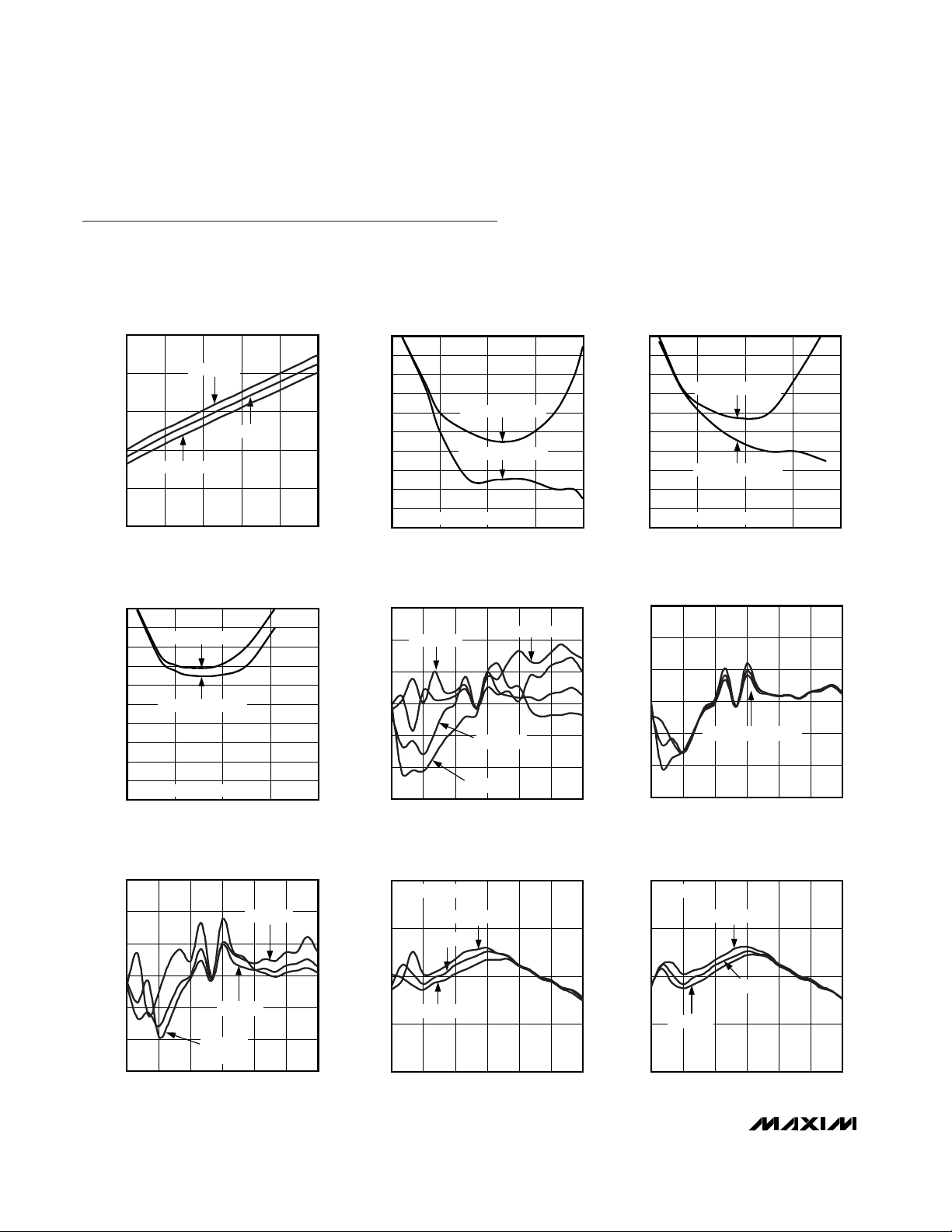
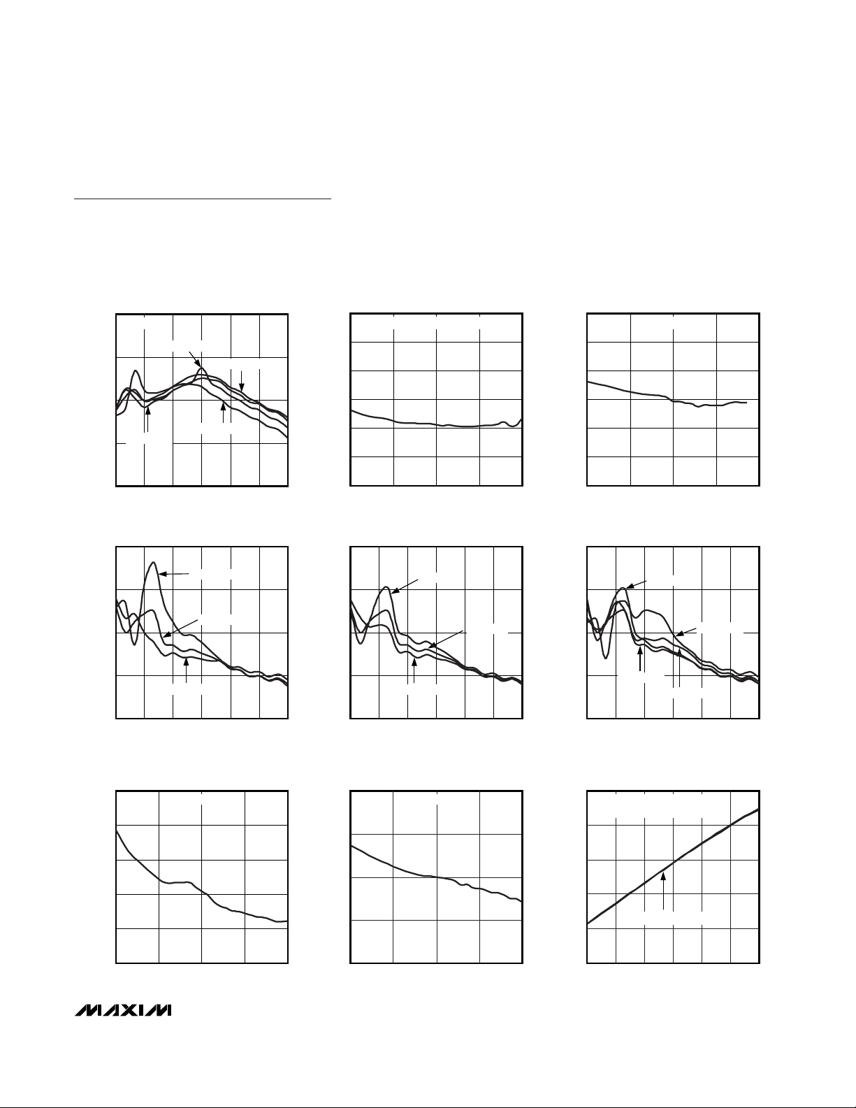
Typical Operating Characteristics
(MAX2021 Typical Application Circuit, VCC= +4.75V to +5.25V, GND = 0V, I/Q differential inputs driven from a 100Ω DC-coupled
source, 0V common-mode input, PLO= 0dBm, 750MHz ≤ fLO≤ 1200MHz, 50Ω LO and RF system impedance, R1 = 432Ω, R2 = 619Ω,
R3 = 332Ω, TC= -40°C to +85°C. Typical values are at VCC= +5V, V
BBI
= 1.4V
P-P
differential, V
BBQ
= 1.4V
P-P
differential, fIQ= 1MHz,
fLO= 900MHz, TC= +25°C, unless otherwise noted.)
TOTAL SUPPLY CURRENT
vs. TEMPERATURE (T
C
)
MAX2021 toc01
TEMPERATURE (°C)
TOTAL SUPPLY CURRENT (mA)
603510-15
220
240
260
280
VCC = 4.75V
VCC = 5.0V
300
200
-40 85
VCC = 5.25V
ACLR vs. OUTPUT POWER PER CARRIER
MAX2021 toc02
OUTPUT POWER PER CARRIER (dBm)
ACLR (dB)
-17-27-37
-78
-76
-74
-72
-70
-68
-66
-64
-62
-60
-80
-47 -7
SINGLE-CARRIER WCDMA
ADJACENT CHANNEL
ALTERNATE CHANNEL
ACLR vs. OUTPUT POWER PER CARRIER
MAX2021 toc03
OUTPUT POWER PER CARRIER (dBm)
ACLR (dB)
-17-27-37
-78
-76
-74
-72
-70
-68
-66
-64
-62
-60
-80
-47 -7
ADJACENT CHANNEL
ALTERNATE CHANNEL
TWO-CARRIER WCDMA
ACLR vs. OUTPUT POWER PER CARRIER
MAX2021 toc04
OUTPUT POWER PER CARRIER (dBm)
ACLR (dB)
-17-27-37
-78
-76
-74
-72
-70
-68
-66
-64
-62
-60
-80
-47 -7
FOUR-CARRIER WCDMA
ADJACENT CHANNEL
ALTERNATE CHANNEL
SIDEBAND SUPPRESSION
vs. LO FREQUENCY
MAX2021 toc05
LO FREQUENCY (MHz)
SIDEBAND SUPPRESSION (dBc)
11251050975900825
20
30
40
50
60
70
10
750 1200
PLO = -3dBm
PLO = -6dBm
PLO = 0dBm
PLO = +3dBm
SIDEBAND SUPPRESSION
vs. LO FREQUENCY
MAX2021 toc06
LO FREQUENCY (MHz)
SIDEBAND SUPPRESSION (dBc)
11251050975900825
20
30
40
50
60
70
10
750 1200
VCC = 4.75V, 5.0V, 5.25V
SIDEBAND SUPPRESSION
vs. LO FREQUENCY
MAX2021 toc07
LO FREQUENCY (MHz)
SIDEBAND SUPPRESSION (dBc)
11251050975900825
20
30
40
50
60
70
10
750 1200
TC = +25°C
TC = +85°C
TC = -40°C
OUTPUT IP3 vs. LO FREQUENCY
MAX2021 toc08
LO FREQUENCY (MHz)
OUTPUT IP3 (dBm)
11251050975900825
15
20
25
30
10
750 1200
TC = -40°C
TC = +85°C
TC = +25°C
PLO = 0dBm, V
CC
= 5.0V
OUTPUT IP3 vs. LO FREQUENCY
MAX2021 toc09
LO FREQUENCY (MHz)
OUTPUT IP3 (dBm)
11251050975900825
15
20
25
30
10
750 1200
VCC = 5.25V
VCC = 5.0V
VCC = 4.75V
TC = +25°C
MODULATOR
Page 5
MAX2021
High-Dynamic-Range, Direct Up-/Downconversion
750MHz to 1200MHz Quadrature Mod/Demod
_______________________________________________________________________________________ 5
OUTPUT IP3 vs. LO FREQUENCY
MAX2021 toc10
LO FREQUENCY (MHz)
OUTPUT IP3 (dBm)
11251050975900825
15
20
25
30
10
750 1200
PLO = +3dBm
PLO = -3dBm
PLO = -6dBm
PLO = 0dBm
TC = +25°C
OUTPUT IP3
vs. COMMON-MODE VOLTAGE
MAX2021 toc11
COMMON-MODE VOLTAGE (V)
OUTPUT IP3 (dBm)
1.750-1.75
21
22
23
24
25
26
20
-3.50 3.50
fLO = 900MHz, PLO = 0dBm
OUTPUT IP3
vs. COMMON-MODE VOLTAGE
MAX2021 toc12
COMMON-MODE VOLTAGE (V)
OUTPUT IP3 (dBm)
1.750-1.75
21
22
23
24
25
26
20
-3.50 3.50
fLO = 1000MHz
OUTPUT IP2 vs. LO FREQUENCY
MAX2021 toc13
LO FREQUENCY (MHz)
OUTPUT IP2 (dBm)
11251050975900825
50
60
70
80
40
750 1200
TC = +25°C
TC = -40°C
TC = +85°C
OUTPUT IP2 vs. LO FREQUENCY
MAX2021 toc14
LO FREQUENCY (MHz)
OUTPUT IP2 (dBm)
11251050975900825
50
60
70
80
40
750 1200
VCC = 5.0V
VCC = 5.25V
VCC = 4.75V
OUTPUT IP2 vs. LO FREQUENCY
MAX2021 toc15
LO FREQUENCY (MHz)
OUTPUT IP2 (dBm)
11251050975900825
50
60
70
80
40
750 1200
PLO = +3dBm
PLO = -6dBm
PLO = -3dBm
PLO = 0dBm
OUTPUT IP2
vs. COMMON-MODE VOLTAGE
MAX2021 toc16
COMMON-MODE VOLTAGE (V)
OUTPUT IP2 (dBm)
1.750-1.75
60
65
70
75
80
55
-3.50 3.50
fLO = 900MHz
OUTPUT IP2
vs. COMMON-MODE VOLTAGE
MAX2021 toc17
COMMON-MODE VOLTAGE (V)
OUTPUT IP2 (dBm)
1.750-1.75
60
55
65
70
50
-3.50 3.50
fLO = 1000MHz
MODULATOR OUTPUT POWER
vs. INPUT POWER
MAX2021 toc18
INPUT POWER (dBm)
OUTPUT POWER (dBm)
1916 252213
10
5
0
15
20
-5
10 28
INPUT SPLIT BETWEEN I AND Q,
f
IF
= 25MHz, fLO = 900MHz
VCC = 4.75V, 5.0V, 5.25V
Typical Operating Characteristics (continued)
(MAX2021 Typical Application Circuit, VCC= +4.75V to +5.25V, GND = 0V, I/Q differential inputs driven from a 100Ω DC-coupled
source, 0V common-mode input, PLO= 0dBm, 750MHz ≤ fLO≤ 1200MHz, 50Ω LO and RF system impedance, R1 = 432Ω, R2 = 619Ω,
R3 = 332Ω, TC= -40°C to +85°C. Typical values are at VCC= +5V, V
BBI
= 1.4V
P-P
differential, V
BBQ
= 1.4V
P-P
differential, fIQ= 1MHz,
fLO= 900MHz, TC= +25°C, unless otherwise noted.)
MODULATOR
Page 6

MAX2021
High-Dynamic-Range, Direct Up-/Downconversion
750MHz to 1200MHz Quadrature Mod/Demod
6 _______________________________________________________________________________________
MODULATOR OUTPUT POWER
vs. INPUT POWER
MAX2021 toc19
INPUT POWER (dBm)
OUTPUT POWER (dBm)
1916 252213
10
5
0
15
20
-5
10 28
INPUT SPLIT BETWEEN I AND Q,
f
IF
= 25MHz, fLO = 900MHz
PLO = -6dBm, -3dBm, 0dBm, +3dBm
MODULATOR OUTPUT POWER
vs. LO FREQUENCY
MAX2021 toc20
LO FREQUENCY (MHz)
OUTPUT POWER (dBm)
975900 11251050825
1
-1
-3
3
5
-5
750 1200
TC = -40°C
TC = +85°C
TC = +25°C
V
BBI
= V
BBQ
= 1.4V
P-P
DIFFERENTIAL
LO LEAKAGE vs. LO FREQUENCY
MAX2021 toc21
LO FREQUENCY (MHz)
LO LEAKAGE (dBm)
959948937926
-90
-80
-70
-60
-50
-40
-100
915 970
PRF = -40dBm
PRF = -7dBm
PRF = -1dBm
LO LEAKAGE NULLED AT PRF = -1dBm
PRF = +5dBm
LO LEAKAGE vs. LO FREQUENCY
MAX2021 toc22
LO FREQUENCY (MHz)
LO LEAKAGE (dBm)
959948937926
-90
-80
-70
-60
-50
-40
-100
915 970
TC = -40°C
TC = +85°C
TC = +25°C
PRF = -1dBm, LO LEAKAGE NULLED AT TC = +25°C
LO LEAKAGE vs. LO FREQUENCY
MAX2021 toc23
LO FREQUENCY (MHz)
LO LEAKAGE (dBm)
959948937926
-90
-80
-70
-60
-50
-40
-100
915 970
PLO = -6dBm
PLO = +3dBm
PLO = -3dBm
PLO = 0dBm
PRF = -1dBm, LO LEAKAGE NULLED AT PLO = 0dBm
OUTPUT NOISE vs. OUTPUT POWER
MAX2021 toc24
OUTPUT POWER (dBm)
OUTPUT NOISE (dBm/Hz)
1050-5-10
-175
-170
-165
-160
-155
-150
-180
-15 15
TC = +25°C, fLO = 900MHz
PLO = -6dBm
PLO = -3dBm
PLO = 0dBm
PLO = +3dBm
OUTPUT NOISE vs. OUTPUT POWER
MAX2021 toc25
OUTPUT POWER (dBm)
OUTPUT NOISE (dBm/Hz)
1050-5-10
-175
-170
-165
-160
-155
-150
-180
-15 15
PLO = 0dBm, fLO = 900MHz
TC = +85°C
TC = -40°C
TC = +25°C
Typical Operating Characteristics (continued)
(MAX2021 Typical Application Circuit, VCC= +4.75V to +5.25V, GND = 0V, I/Q differential inputs driven from a 100Ω DC-coupled
source, 0V common-mode input, PLO= 0dBm, 750MHz ≤ fLO≤ 1200MHz, 50Ω LO and RF system impedance, R1 = 432Ω, R2 = 619Ω,
R3 = 332Ω, TC= -40°C to +85°C. Typical values are at VCC= +5V, V
BBI
= 1.4V
P-P
differential, V
BBQ
= 1.4V
P-P
differential, fIQ= 1MHz,
fLO= 900MHz, TC= +25°C, unless otherwise noted.)
MODULATOR
Page 7

MAX2021
High-Dynamic-Range, Direct Up-/Downconversion
750MHz to 1200MHz Quadrature Mod/Demod
_______________________________________________________________________________________ 7
DEMODULATOR CONVERSION LOSS
vs. LO FREQUENCY
MAX2021 toc26
LO FREQUENCY (MHz)
DEMODULATOR CONVERSION LOSS (dB)
975900 11251050825
10
9
8
11
12
7
750 1200
PLO = 0dBm, VCC = 5.0V
TC = +85°C
TC = +25°C
TC = -40°C
DEMODULATOR INPUT IP3
vs. LO FREQUENCY
MAX2021 toc27
LO FREQUENCY (MHz)
DEMODULATOR INPUT IP3 (dBm)
975900 11251050825
36
34
32
38
40
30
750 1200
PLO = 0dBm, TC = +25°C
VCC = 4.75V
VCC = 5.25V
VCC = 5.0V
DEMODULATOR INPUT IP3
vs. LO FREQUENCY
MAX2021 toc28
LO FREQUENCY (MHz)
DEMODULATOR INPUT IP3 (dBm)
975900 11251050825
36
34
32
38
40
30
750 1200
PLO = 0dBm, VCC = 5.0V
TC = +85°C
TC = +25°C
TC = -40°C
DEMODULATOR INPUT IP2
vs. LO FREQUENCY
MAX2021 toc29
LO FREQUENCY (MHz)
DEMODULATOR INPUT IP2 (dBm)
11251050975900825
60
70
80
90
50
750 1200
TC = -40°C
TC = +85°C
TC = +25°C
PLO = 0dBm, V
CC
= 5.0V
DEMODULATOR PHASE IMBALANCE
vs. LO FREQUENCY
MAX2021 toc30
DEMODULATOR PHASE IMBALANCE (deg)
-8
-6
-4
-2
0
2
4
6
8
10
-10
LO FREQUENCY (MHz)
11251050975900825750 1200
PLO = -3dBm
PLO = 0dBm
PLO = +3dBm
PLO = -6dBm
MAX2021 toc31
-0.15
-0.10
-0.05
0
0.05
0.10
0.15
0.20
-0.20
DEMODULATOR AMPLITUDE IMBALANCE
vs. LO FREQUENCY
DEMODULATOR AMPLITUDE IMBALANCE (dB)
LO FREQUENCY (MHz)
11251050975900825750 1200
PLO = -6dBm, -3dBm, 0dBm, +3dBm
Typical Operating Characteristics
(MAX2021 Typical Application Circuit, VCC= +4.75V to +5.25V, GND = 0V, I/Q differential inputs driven from a 100Ω DC-coupled
source, 0V common-mode input, PRF= 5dBm, PLO= 0dBm, 750MHz ≤ fLO≤ 1200MHz, 50Ω LO and RF system impedance, R1 = 432Ω,
R2 = 619Ω, R3 = 332Ω, TC= -40°C to +85°C. Typical values are at VCC= +5V, fLO= 900MHz, TC= +25°C, unless otherwise noted.)
LO PORT RETURN LOSS
vs. LO FREQUENCY
MAX2021 toc32
LO FREQUENCY (MHz)
LO PORT RETURN LOSS (dB)
975900 11251050825
+10
+15
+20
+5
0
+25
750 1200
PLO = -6dBm, -3dBm
PLO = +3dBm
PLO = 0dBm
RF PORT RETURN LOSS
vs. LO FREQUENCY
MAX2021 toc33
LO FREQUENCY (MHz)
RF PORT RETURN LOSS (dB)
11301035940845
+40
+35
+30
+25
+20
+15
+10
+5
0
+45
750 1225
PLO = -6dBm, -3dBm, 0dBm, +3dBm
IF FLATNESS
vs. BASEBAND FREQUENCY
MAX2021 toc34
BASEBAND FREQUENCY (MHz)
IF OUTPUT POWER (dBm)
706010 20 30 40 50
-11
-10
-9
-8
-7
-6
-5
-4
-12
080
fLO = 1000MHz
fLO = 900MHz
PLO = 0dBm
DEMODULATOR
Page 8

MAX2021
High-Dynamic-Range, Direct Up-/Downconversion
750MHz to 1200MHz Quadrature Mod/Demod
8 _______________________________________________________________________________________
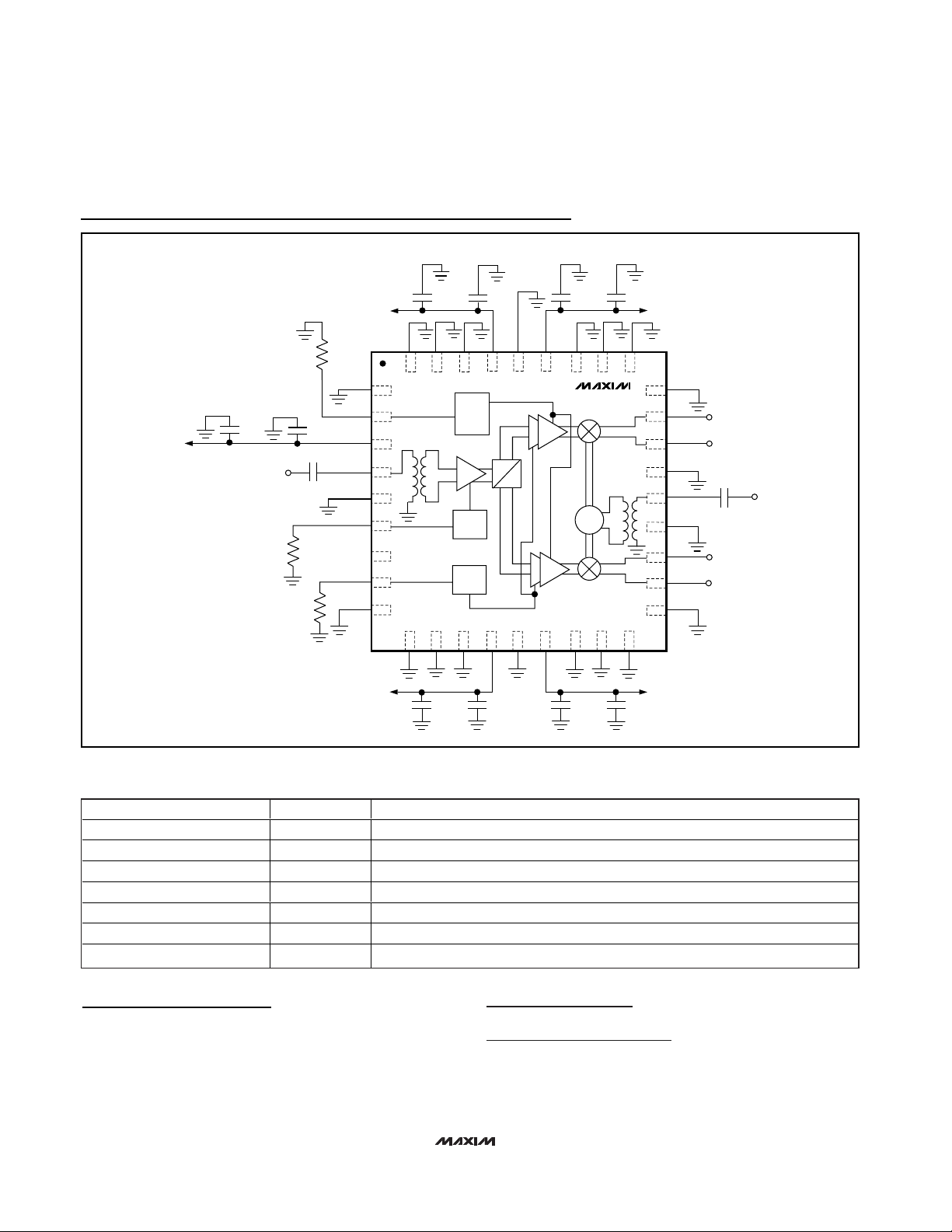
Detailed Description
The MAX2021 is designed for upconverting differential
in-phase (I) and quadrature (Q) inputs from baseband
to a 750MHz to 1200MHz RF frequency range. The
device can also be used as a demodulator, downconverting an RF input signal directly to baseband.
Applications include RFID handheld and portal readers,
as well as single and multicarrier GSM/EDGE,
cdma2000, WCDMA, and iDEN base stations. Direct
conversion architectures are advantageous since they
significantly reduce transmitter or receiver cost, part
count, and power consumption as compared to traditional IF-based double conversion systems.
The MAX2021 integrates internal baluns, an LO buffer, a
phase splitter, two LO driver amplifiers, two matched
double-balanced passive mixers, and a wideband
quadrature combiner. The MAX2021’s high-linearity mixers, in conjunction with the part’s precise in-phase and
quadrature channel matching, enable the device to possess excellent dynamic range, ACLR, 1dB compression
point, and LO and sideband suppression characteristics. These features make the MAX2021 ideal for fourcarrier WCDMA operation.
LO Input Balun, LO Buffer, and
Phase Splitter
The MAX2021 requires a single-ended LO input, with a
nominal power of 0dBm. An internal low-loss balun at
the LO input converts the single-ended LO signal to a
differential signal at the LO buffer input. In addition, the
internal balun matches the buffer’s input impedance to
50Ω over the entire band of operation.
The output of the LO buffer goes through a phase splitter, which generates a second LO signal that is shifted
by 90° with respect to the original. The 0° and 90° LO
signals drive the I and Q mixers, respectively.
LO Driver
Following the phase splitter, the 0° and 90° LO signals
are each amplified by a two-stage amplifier to drive the
I and Q mixers. The amplifier boosts the level of the LO
Pin Description
PIN NAME FUNCTION
1, 5, 9–12, 14, 16–19, 22,
24, 27–30, 32, 34, 35, 36
GND Ground
2
3rd LO Amplifier Bias. Connect a 332Ω resistor to ground.
3
LO Input Buffer Amplifier Supply Voltage. Bypass to GND with 33pF and 0.1µF
capacitors as close to the pin as possible.
4 LO Local Oscillator Input. 50Ω input impedance.
6
1st LO Input Buffer Amplifier Bias. Connect a 432Ω resistor to ground.
7 N.C. No Connection. Leave unconnected.
8
2nd LO Amplifier Bias. Connect a 619Ω resistor to ground.
13
I-Channel 1st LO Amplifier Supply Voltage. Bypass to GND with 33pF and 0.1µF
capacitors as close to the pin as possible.
15
I-Channel 2nd LO Amplifier Supply Voltage. Bypass to GND with 33pF and 0.1µF
capacitors as close to the pin as possible.
20 BBI+ Baseband In-Phase Noninverting Port
21 BBI- Baseband In-Phase Inverting Port
23 RF RF Port
25 BBQ- Baseband Quadrature Inverting Port
26 BBQ+ Baseband Quadrature Noninverting Port
31
Q-Channel 2nd LO Amplifier Supply Voltage. Bypass to GND with 33pF and 0.1µF
capacitors as close to the pin as possible.
33
Q-Channel 1st LO Amplifier Supply Voltage. Bypass to GND with 33pF and 0.1µF
capacitors as close to the pin as possible.
EP GND
Exposed Ground Paddle. The exposed paddle MUST be soldered to the ground plane
using multiple vias.
RBIASLO3
VCCLOA
RBIASLO1
RBIASLO2
VCCLOI1
VCCLOI2
VCCLOQ2
VCCLOQ1
Page 9

MAX2021
High-Dynamic-Range, Direct Up-/Downconversion
750MHz to 1200MHz Quadrature Mod/Demod
signals to compensate for any changes in LO drive levels. The two-stage LO amplifier allows a wide input
power range for the LO drive. The MAX2021 can tolerate LO level swings from -6dBm to +3dBm.
I/Q Modulator
The MAX2021 modulator is composed of a pair of
matched double-balanced passive mixers and a balun.
The I and Q differential baseband inputs accept signals
from DC to 300MHz with differential amplitudes up to
4V
P-P
. The wide input bandwidths allow operation of the
MAX2021 as either a direct RF modulator or as an
image-reject mixer. The wide common-mode compliance range allows for direct interface with the baseband DACs. No active buffer circuitry is required
between the baseband DACs and the MAX2021 for
cdma2000 and WCDMA applications.
The I and Q signals directly modulate the 0° and 90° LO
signals and are upconverted to the RF frequency. The outputs of the I and Q mixers are combined through a balun
to produce a singled-ended RF output.
Applications Information
LO Input Drive
The LO input of the MAX2021 is internally matched to
50Ω, and requires a single-ended drive at a 750MHz to
1200MHz frequency range. An integrated balun converts the singled-ended input signal to a differential signal at the LO buffer differential input. An external
DC-blocking capacitor is the only external part required
at this interface. The LO input power should be within
the -6dBm to +3dBm range. An LO input power of
-3dBm is recommended for best overall peformance.
Baseband I/Q Input Drive
Drive the MAX2021 I and Q baseband inputs differentially for best performance. The baseband inputs have
a 53Ω differential input impedance. The optimum
source impedance for the I and Q inputs is 100Ω differential. This source impedance achieves the optimal signal transfer to the I and Q inputs, and the optimum
output RF impedance match. The MAX2021 can accept
input power levels of up to +20dBm on the I and Q
inputs. Operation with complex waveforms, such as
CDMA carriers or GSM signals, utilize input power levels that are far lower. This lower power operation is
made necessary by the high peak-to-average ratios of
these complex waveforms. The peak signals must be
kept below the compression level of the MAX2021. The
input common-mode voltage should be confined to the
-3.5V to +3.5V DC range.
The MAX2021 is designed to interface directly with
Maxim high-speed DACs. This generates an ideal total
transmitter lineup, with minimal ancillary circuit elements.
Such DACs include the MAX5875 series of dual DACs,
and the MAX5895 dual interpolating DAC. These DACs
have ground-referenced differential current outputs.
Typical termination of each DAC output into a 50Ω load
resistor to ground, and a 10mA nominal DC output current results in a 0.5V common-mode DC level into the
modulator I/Q inputs. The nominal signal level provided
by the DACs will be in the -12dBm range for a single
CDMA or WCDMA carrier, reducing to -18dBm per carrier for a four-carrier application.
The I/Q input bandwidth is greater than 50MHz at
-0.1dB response. The direct connection of the DAC to
the MAX2021 ensures the maximum signal fidelity, with
no performance-limiting baseband amplifiers required.
The DAC output can be passed through a lowpass filter
to remove the image frequencies from the DAC’s output
response. The MAX5895 dual interpolating DAC can be
operated at interpolation rates up to x8. This has the
benefit of moving the DAC image frequencies to a very
high, remote frequency, easing the design of the baseband filters. The DAC’s output noise floor and interpolation filter stopband attenuation are sufficiently good to
ensure that the 3GPP noise floor requirement is met for
large frequency offsets, 60MHz for example, with no filtering required on the RF output of the modulator.
Figure 1 illustrates the ease and efficiency of interfacing
the MAX2021 with a Maxim DAC, in this case the
MAX5895 dual 16-bit interpolating-modulating DAC.
MAX5895
DUAL 16-BIT INTERP DAC
RF MODULATOR
I/Q GAIN AND
OFFSET ADJUST
BBI
LO
BBQ
FREQ
50Ω
50Ω
FREQ
50Ω
50Ω
0°
90°
∑
MAX2021
Figure 1. MAX5895 DAC Interfaced with MAX2021
_______________________________________________________________________________________________________ 9
Page 10

MAX2021
High-Dynamic-Range, Direct Up-/Downconversion
750MHz to 1200MHz Quadrature Mod/Demod
10 ______________________________________________________________________________________
MAX2021MAX2021
The MAX5895 DAC has programmable gain and differential offset controls built in. These can be used to optimize the LO leakage and sideband suppression of the
MAX2021 quadrature modulator.
RF Output
The MAX2021 utilizes an internal passive mixer architecture that enables the device to possess an exceptionally low-output noise floor. With such architectures,
the total output noise is typically a power summation of
the theoretical thermal noise (KTB) and the noise contribution from the on-chip LO buffer circuitry. As demonstrated in the Typical Operating Characteristics, the
MAX2021’s output noise approaches the thermal limit
of -174dBm/Hz for lower output power levels. As the
output power increases, the noise level tracks the noise
contribution from the LO buffer circuitry, which is
approximately -168dBc/Hz.
The I/Q input power levels and the insertion loss of the
device determine the RF output power level. The input
power is a function of the delivered input I and Q voltages to the internal 50Ω termination. For simple sinusoidal baseband signals, a level of 89mV
P-P
differential
on the I and the Q inputs results in a -17dBm input
power level delivered to the I and Q internal 50Ω termi-
nations. This results in an RF output power of -23.2dBm.
External Diplexer
LO leakage at the RF port can be nulled to a level less
than -80dBm by introducing DC offsets at the I and Q
ports. However, this null at the RF port can be compro-
mised by an improperly terminated I/Q IF interface. Care
must be taken to match the I/Q ports to the driving DAC
circuitry. Without matching, the LO’s second-order (2fLO)
term may leak back into the modulator’s I/Q input port
where it can mix with the internal LO signal to produce
additional LO leakage at the RF output. This leakage
effectively counteracts against the LO nulling. In addition, the LO signal reflected at the I/Q IF port produces a
residual DC term that can disturb the nulling condition.
As demonstrated in Figure 2, providing an RC termination
on each of the I+, I-, Q+, Q- ports reduces the amount of
LO leakage present at the RF port under varying temperature, LO frequency, and baseband drive conditions. See
the Typical Operating Characteristics for details. Note
that the resistor value is chosen to be 100Ω with a corner
frequency 1 / (2πRC) selected to adequately filter the f
LO
and 2fLOleakage, yet not affecting the flatness of the
baseband response at the highest baseband frequency.
The common-mode fLOand 2fLOsignals at I+/I- and
Q+/Q- effectively see the RC networks and thus become
terminated in 50Ω (R/2). The RC network provides a path
for absorbing the 2fLOand fLOleakage, while the inductor provides high impedance at fLOand 2fLOto help the
diplexing process.
RF Demodulator
The MAX2021 can also be used as an RF demodulator,
downconverting an RF input signal directly to baseband. The single-ended RF input accepts signals from
750MHz to 1200MHz with power levels up to +30dBm.
The passive mixer architecture produces a conversion
loss of typically 9.2dB. The downconverter is optimized
for high linearity and excellent noise performance, typically with a +35.2dBm IIP3, a P1dB of greater than
+30dBm, and a 9.3dB noise figure.
A wide I/Q port bandwidth allows the port to be used as
an image-reject mixer for downconversion to a quadrature IF frequency.
The RF and LO inputs are internally matched to 50Ω.
Thus, no matching components are required, and only
DC-blocking capacitors are needed for interfacing.
Power Scaling with Changes
to the Bias Resistors
Bias currents for the LO buffers are optimized by fine
tuning resistors R1, R2, and R3. Maxim recommends
using ±1%-tolerant resistors; however, standard ±5%
values can be used if the ±1% components are not
readily available. The resistor values shown in the
Typical Application Circuit were chosen to provide
peak performance for the entire 750MHz to 1200MHz
band. If desired, the current can be backed off from
this nominal value by choosing different values for R1,
RF-MODULATOR
LO
100Ω
100Ω
L = 40nH
C = 6.8pF
∑
L = 40nH
I
Q
100Ω
100Ω
C = 6.8pF
C = 6.8pF
0°
90°
MAX2021
Figure 2. Diplexer Network Recommended for GSM 900
Transmitter Applications
Page 11

MAX2021
High-Dynamic-Range, Direct Up-/Downconversion
750MHz to 1200MHz Quadrature Mod/Demod
______________________________________________________________________________________ 11
R2, and R3. Tables 1 and 2 outline the performance
trade-offs that can be expected for various combinations of these bias resistors. As noted within the tables,
the performance trade-offs may be more pronounced
for different operating frequencies. Contact the factory
for additional details.
Layout Considerations
A properly designed PC board is an essential part of
any RF/microwave circuit. Keep RF signal lines as short
as possible to reduce losses, radiation, and inductance. For the best performance, route the ground pin
traces directly to the exposed pad under the package.
The PC board exposed paddle MUST be connected to
the ground plane of the PC board. It is suggested that
multiple vias be used to connect this pad to the lowerlevel ground planes. This method provides a good
RF/thermal conduction path for the device. Solder the
exposed pad on the bottom of the device package to
the PC board. The MAX2021 evaluation kit can be used
as a reference for board layout. Gerber files are available upon request at www.maxim-ic.com.
Power-Supply Bypassing
Proper voltage-supply bypassing is essential for highfrequency circuit stability. Bypass all VCC_ pins with
33pF and 0.1µF capacitors placed as close to the pins
as possible. The smallest capacitor should be placed
closest to the device.
To achieve optimum performance, use good voltagesupply layout techniques. The MAX2021 has several RF
processing stages that use the various VCC_ pins, and
while they have on-chip decoupling, off-chip interaction
between them may degrade gain, linearity, carrier suppression, and output power-control range. Excessive
coupling between stages may degrade stability.
Exposed Pad RF/Thermal Considerations
The EP of the MAX2021’s 36-pin thin QFN-EP package
provides a low thermal-resistance path to the die. It is
important that the PC board on which the IC is mounted
be designed to conduct heat from this contact. In addition, the EP provides a low-inductance RF ground path
for the device.
The exposed paddle (EP) MUST be soldered to a
ground plane on the PC board either directly or through
an array of plated via holes. An array of 9 vias, in a 3 x
3 array, is suggested. Soldering the pad to ground is
critical for efficient heat transfer. Use a solid ground
plane wherever possible.
Note: VCC= 5V, PLO= 0dBm, TA= +25°C, I/Q voltage levels = 1.4V
P-P
differential.
LO FREQ
(MHz)
RF FREQ
(MHz)
R1
(ΩΩΩΩ)
R2
(ΩΩΩΩ)
R3
(ΩΩΩΩ)
I
CC
(mA)
OIP3
(dBm)
LO LEAK
(dBm)
IMAGE REJ
(dBc)
OIP2
(dBm)
420 620 330 271 19.6 -32.1 23.9 50.5
453 665 360 253 21.9 -32.7 34.0 51.0
499 698 402 229 18.9 -33.7 30.0 52.6
549 806 464 205 15.7 -34.4 23.7 46.0
800 801.8
650 1000 550 173 13.6 -34.2 23.3 32.3
420 620 330 271 20.7 -31.4 43.4 54.0
453 665 360 253 21.6 -31.6 42.4 55.4
499 698 402 229 20.6 -31.8 42.7 59.8
549 806 464 205 19.0 -31.9 40.3 50.7
900 901.8
650 1000 550 173 14.9 -30.5 25.0 34.6
420 620 330 271 22.4 -32.8 39.3 55.5
453 665 360 253 22.2 -33.2 39.1 56.3
499 698 402 229 19.9 -33.8 43.5 55.0
549 806 464 205 17.6 -34.8 40.5 51.4
1000
650 1000 550 173 14.6 -33.9 36.8 32.8
Table 1. Typical Performance Trade-Offs as a Function of Current Draw—Modulator Mode
1001.8
Page 12

MAX2021
High-Dynamic-Range, Direct Up-/Downconversion
750MHz to 1200MHz Quadrature Mod/Demod
12 ______________________________________________________________________________________
LO FREQ
(MHz)
RF FREQ
(MHz)
R1
(ΩΩΩΩ)
R2
(ΩΩΩΩ)
R3
(ΩΩΩΩ)
I
CC
(mA)
C O N VER SIO N
L O SS ( d B )
IIP3
(dBm)
57MHz IIP2
(dBm)
420 620 330 269 9.8 33.85 62.1
453 665 360 254 9.83 33.98 62.9
499 698 402 230 9.81 32.2 66.6
549 806 464 207 9.84 31.1 66.86
800 771
650 1000 550 173 9.95 29.87 65.25
420 620 330 269 9.21 33.1 68
453 665 360 254 9.25 33.9 66.87
499 698 402 230 9.36 34.77 66.7
549 806 464 207 9.39 35.3 66.6
900 871
650 1000 550 173 9.46 32 64.64
420 620 330 269 9.47 34.9 > 77.7
453 665 360 254 9.5 35.4 > 77.5
499 698 402 230 9.53 34.58 > 76.5
549 806 464 207 9.5 33.15 > 76.5
1000 971
650 1000 550 173 9.61 31.5 76
Table 2. Typical Performance Trade-Offs as a Function of Current Draw—Demodulator Mode
Note: Used on PC board 180° combiners and off PC board quadrature combiner with VCC= 5V, PRF= -3dBm, P
LO
= 0dBm, TA = +25°C,
IF1 = 28MHz, IF2 = 29MHz.
Page 13

MAX2021
High-Dynamic-Range, Direct Up-/Downconversion
750MHz to 1200MHz Quadrature Mod/Demod
______________________________________________________________________________________ 13
MAX2021
1
2
3
4
5
6
7
8
9
10
11 12
13 14
THIN QFN
15
16 17
18
27
26
25
24
23
22
21
20
19
36
35
34
33 32
31
30 29
28
Σ
BIAS
LO2
BIAS
LO1
90°
0°
BIAS
LO3
GND
BBI+
BBI-
GND
RF
GND
BBQ-
BBQ+
GND
GND
GND
GND
GND
GND
GND
GND
GND
GND
RBIASLO3
VCCLOA
LO
GND
RBIASLO1
N.C.
RBIASLO2
GND
GND
GND
VCCLOQ2
GND
GND
GND
GND
MAX2021
VCCLOI1
VCCLOI2
VCCLOQ1
Pin Configuration/Functional Diagram
Page 14
1
2
3
4
5
6
7
8
9
10
11 12
13 14 15
16 17
18
27
26
25
24
23
22
21
20
19
36
35
34
33 32
31
30 29
28
Σ
BIAS
LO2
BIAS
LO1
90°
0°
BIAS
LO3
GND
BBI+
BBI-
GND
RF
RF
GND
BBQ-
BBQ+
Q+
Q-
GND
I-
I+
C9
8.2pF
C8
0.1μF
V
CC
C7
33pF
C5
0.1μF
C6
33pF
V
CC
GND
GND
GND
GND
VCCLOI1
VCCLOI2
GND
GND
GND
GND
GND
RBIASLO3
R3
332Ω
C1
33pF
C3
82pF
C2
0.1μF
V
CC
VCCLOA
LO
GND
RBIASLO1
R1
432Ω
N.C.
RBIASLO2
C11
0.1μF
V
CC
C10
33pF
C12
0.1μF
C13
33pF
V
CC
GND
GND
GND
VCCLOQ2
GND
GND
GND
GND
MAX2021
VCCLOQ1
R2
619Ω
Typical Application Circuit
MAX2021
High-Dynamic-Range, Direct Up-/Downconversion
750MHz to 1200MHz Quadrature Mod/Demod
Maxim cannot assume responsibility for use of any circuitry other than circuitry entirely embodied in a Maxim product. No circuit patent licenses are
implied. Maxim reserves the right to change the circuitry and specifications without notice at any time.
14 ____________________Maxim Integrated Products, 120 San Gabriel Drive, Sunnyvale, CA 94086 408-737-7600
© 2006 Maxim Integrated Products Printed USA is a registered trademark of Maxim Integrated Products, Inc.
COMPONENT VALUE DESCRIPTION
C1, C6, C7, C10, C13 33pF 33pF ±5%, 50V C0G ceramic capacitors (0402)
C2, C5, C8, C11, C12 0.1µF 0.1µF ±10%, 16V X7R ceramic capacitors (0603)
C3 82pF 82pF ±5%, 50V C0G ceramic capacitor (0402)
C9 8.2pF 8.2pF ±0.1pF, 50V C0G ceramic capacitor (0402)
R1 432Ω 432Ω ±1% resistor (0402)
R2 619Ω 619Ω ±1% resistor (0402)
R3 332Ω 332Ω ±1% resistor (0402)
Table 3. Component List Referring to the Typical Application Circuit
Package Information
For the latest package outline information, go to
www.maxim-ic.com/packages
.
Chip Information
PROCESS: SiGe BiCMOS
 Loading...