

Page 1
General Description
The MAX2016 dual logarithmic detector/controller is a
fully integrated system designed for measuring and
comparing power, gain/loss, and voltage standing-wave
ratio (VSWR) of two incoming RF signals. An internal
broadband impedance match on the two differential RF
input ports allows for the simultaneous monitoring of signals ranging from low frequency to 2.5GHz.
The MAX2016 uses a pair of logarithmic amplifiers to
detect and compare the power levels of two RF input
signals. The device internally subtracts one power level
from the other to provide a DC output voltage that is proportional to the power difference (gain). The MAX2016
can also measure the return loss/VSWR of an RF signal
by monitoring the incident and reflected power levels
associated with any given load. A window detector is
easily implemented by using the on-chip comparators,
OR gate, and 2V reference. This combination of circuitry
provides an automatic indication of when the measured
gain is outside a programmable range. Alarm monitoring
can thus be implemented for detecting high-VSWR
states (such as open or shorted loads).
The MAX2016 operates from a single +2.7V to +5.25V*
power supply and is specified over the extended -40°C
to +85°C temperature range. The MAX2016 is available
in a space-saving, 5mm x 5mm, 28-pin thin QFN.
Applications
Return Loss/VSWR Measurements
Dual-Channel RF Power Measurements
Dual-Channel Precision AGC/RF Power Control
Log Ratio Function for RF Signals
Remote System Monitoring and Diagnostics
Cellular Base Station, Microwave Link, Radar,
and other Military Applications
RF/IF Power Amplifier (PA) Linearization
Features
♦ Complete Gain and VSWR Detector/Controller
♦ Dual-Channel RF Power Detector/Controller
♦ Low-Frequency to 2.5GHz Frequency Range
♦ Exceptional Accuracy Over Temperature
♦ High 80dB Dynamic Range
♦ 2.7V to 5.25V Supply Voltage Range*
♦ Internal 2V Reference
♦ Scaling Stable Over Supply and Temperature
Variations
♦ Controller Mode with Error Output
♦ Available in 5mm x 5mm, 28-Pin Thin QFN
Package
*See Power-Supply Connection section.
MAX2016
LF-to-2.5GHz Dual Logarithmic Detector/
Controller for Power, Gain, and VSWR Measurements
________________________________________________________________ Maxim Integrated Products 1
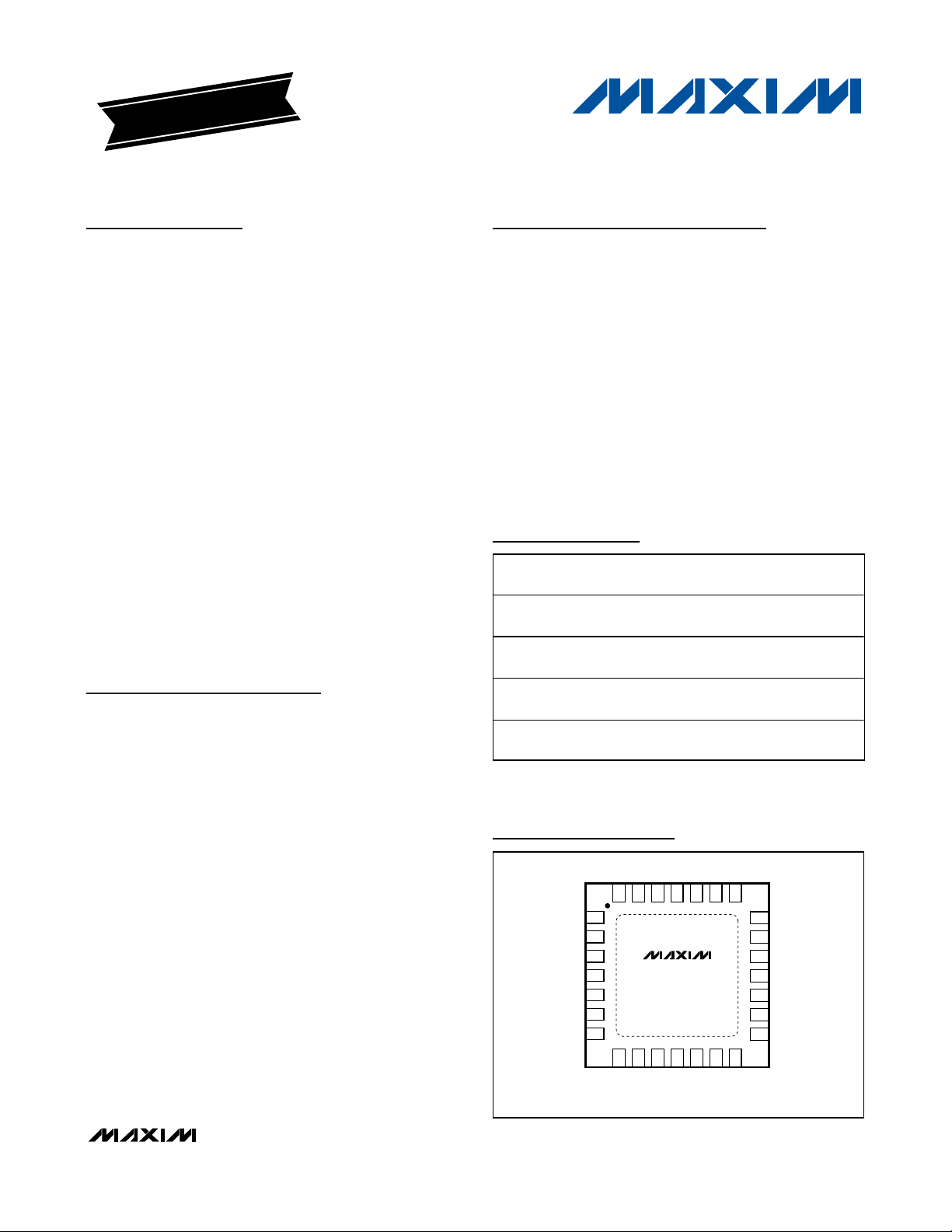
Pin Configuration
Ordering Information
19-3404; Rev 1; 10/06
For pricing, delivery, and ordering information, please contact Maxim/Dallas Direct! at
1-888-629-4642, or visit Maxim’s website at www.maxim-ic.com.
EVALUATION KIT
AVAILABLE
*EP = Exposed pad.
+Indicates lead-free package.
D = Dry pack.
Typical Application Circuit appears at end of data sheet.
PART TEMP RANGE
MAX2016ETI -40°C to +85°C
MAX2016ETI-T -40°C to +85°C
MAX2016ETI+D -40°C to +85°C
MAX2016ETI+TD -40°C to +85°C
PINPACKAGE
28 Thi n QFN - E P *,
b ul k
28 Thi n QFN - E P *,
T/R
28 Thi n QFN - E P *,
l ead fr ee, b ul k
28 Thi n QFN - E P *,
l ead fr ee, T/R
T2855-3
T2855-3
T2855-3
T2855-3
FA228OUTA27SETA26REF25SETB24OUTB23FB2
22
FA1 1
VCC2
RFINA+ 3
RFINA- 4
GND 5
COUTH 6
CSETH 7
MAX2016
8
9
10
11
12
COR
CC
V
THIN QFN
SETD
OUTD
V
CC
FV213FV1
FB121
VCC20
RFINB+19
RFINB-18
GND17
COUTL16
CSETL15
14
PKG
CODE
Page 2
MAX2016
LF-to-2.5GHz Dual Logarithmic Detector/
Controller for Power, Gain, and VSWR Measurements
2 _______________________________________________________________________________________
ABSOLUTE MAXIMUM RATINGS
Stresses beyond those listed under “Absolute Maximum Ratings” may cause permanent damage to the device. These are stress ratings only, and functional
operation of the device at these or any other conditions beyond those indicated in the operational sections of the specifications is not implied. Exposure to
absolute maximum rating conditions for extended periods may affect device reliability.
VCCto GND.........................................................-0.3V to +5.25V
Input Power Differential (RFIN_+, RFIN_-)......................+23dBm
Input Power Single Ended (RFIN_+ or RFIN _-) .............+19dBm
All Other Pins to GND.................................-0.3V to (V
CC
+ 0.3V)
Continuous Power Dissipation (T
A
= +70°C)
28-Pin, 5mm x 5mm Thin QFN (derate 35.7mW/°C
above +70°C)..................................................................2.8W
Operating Temperature Range ...........................-40°C to +85°C
Junction Temperature......................................................+150°C
Storage Temperature Range .............................-65°C to +150°C
Lead Temperature (soldering, 10s) .................................+300°C
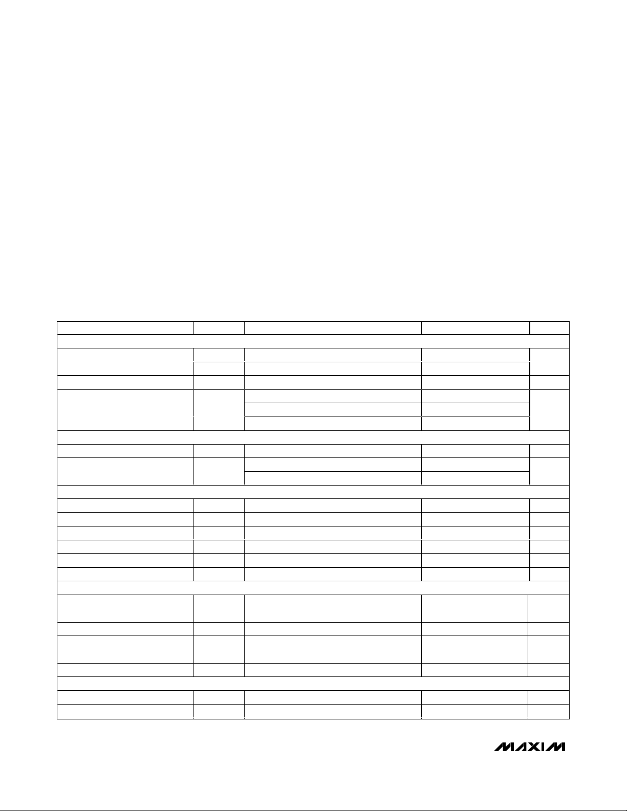
DC ELECTRICAL CHARACTERISTICS
(VCC= +2.7V to +3.6V, R1= R2= R3= 0Ω, TA= -40°C to +85°C, unless otherwise noted. Typical values are at VCC= +3.3V,
CSETL = CSETH = V
CC
, 50Ω RF system, TA= +25°C, unless otherwise noted.) (Note 1)
PARAMETER SYMBOL CONDITIONS MIN TYP MAX UNITS
POWER SUPPLY
Supply Voltage
Total Supply Current I
Supply Current
INPUT INTERFACE
Input Impedance Differential impedance at RFINA and RFINB 50 Ω
Input Resistance R
DETECTOR OUTPUT
Source Current Measured at OUTA, OUTB, and OUTD 4 mA
Sink Current Measured at OUTA, OUTB, and OUTD 0.45 mA
Minimum Output Voltage Measured at OUTA, OUTB, and OUTD 0.5 V
Maximum Output Voltage Measured at OUTA, OUTB, and OUTD 1.8 V
Difference Output VOUTD P
OUTD Accuracy ±12 mV
COMPARATORS
Output High Voltage V
Output Low Voltage V
Input Voltage Measured at CSETL and CSETH
Input Bias Current CSETL and CSETH 1 nA
REFERENCE
Output Voltage on Pin 25 R
Load Regulation Source 2mA -5 mV
V
V
CC
OH
OL
R6 = 0Ω 2.7 3.3 3.6
S
R6 = 37.4Ω 4.75 5 5.25
S
Measured in each pin 2 and pin 20 16
Measured in pin 9 2
Measured in pin 12 9
Resistance at SETD 20
Resistance at SETA and SETB 40
= P
RFINA
R
LOAD
R
LOAD
LOAD
RFINB
≥ 10kΩ
≥ 10kΩ 10 mV
≥ 2kΩ 2V
43 55 mA
= -30dBm 1 V
V
-
CC
10mV
GND to
V
CC
V
mA
kΩ
V
V
Page 3
MAX2016
LF-to-2.5GHz Dual Logarithmic Detector/
Controller for Power, Gain, and VSWR Measurements
_______________________________________________________________________________________ 3
AC ELECTRICAL CHARACTERISTICS—OUTA AND OUTB
(Typical Application Circuit, VCC= +2.7V to +3.3V, R1= R2= R3= 0Ω, TA= -40°C to +85°C, unless otherwise noted. Typical values
are at V
CC
= 3.3V, CSETL = CSETH = VCC, TA= +25°C, unless otherwise noted.) (Note 1)
RF Input Frequency Range f
Return Loss S
Large-Signal Response Time
RSSI MODE—0.1GHz
RF Input Power Range (Note 2)
±3dB Dynamic Range TA = -20°C to +85°C (Note 3) 80 dB
Range Center -32 dBm
Temperature Sensitivity
Slope (Note 4) 19 mV/dB
Typical Slope Variation TA = -20°C to +85°C -4 µV/°C
Intercept (Note 5) -100 dBm
Typical Intercept Variation TA = -20°C to +85°C 0.03 dBm/°C
RSSI MODE—0.9GHz
RF Input Power Range (Note 2)
±3dB Dynamic Range TA = -20°C to +85°C (Note 3) 80 dB
Range Center -30 dBm
Temperature Sensitivity
Slope (Note 4) 18.1 mV/dB
Typical Slope Variation TA = -20°C to +85°C -4 µV/°C
Intercept (Note 5) -97 dBm
Typical Intercept Variation TA = -20°C to +85°C 0.02 dBm/°C
RSSI MODE—1.9GHz
RF Input Power Range (Note 2)
±3dB Dynamic Range TA = -20°C to +85°C (Note 3) 67 dB
Range Center -27 dBm
Temperature Sensitivity
Slope (Note 4) 18 mV/dB
Typical Slope Variation TA = -20°C to +85°C -4.8 µV/°C
Intercept (Note 5) -88 dBm
Typical Intercept Variation TA = -20°C to +85°C 0.03 dBm/°C
PARAMETER SYMBOL CONDITIONS MIN TYP MAX UNITS
RF
AC-coupled input 2.5 GHz
0.1GHz to 3GHz 20 dB
11
P
= no signal to 0dBm, ±0.5dB settling
RFIN
accuracy
P
RFINA
-32dBm
P
RFINA
-30dBm
P
RFINA
-27dBm
= P
= P
= P
RFINB
RFINB
RFINB
TA = +25°C to +85°C +0.0083
=
= +25°C to -20°C -0.0083
T
A
TA = +25°C to +85°C +0.0083
=
= +25°C to -20°C -0.0083
T
A
TA = +25°C to +85°C +0.0125
=
= +25°C to -20°C -0.0125
T
A
100 ns
-70 to
+10
-70 to
+10
-55 to
+12
dBm
dB/°C
dBm
dB/°C
dBm
dB/°C
Page 4
MAX2016
LF-to-2.5GHz Dual Logarithmic Detector/
Controller for Power, Gain, and VSWR Measurements
4 _______________________________________________________________________________________
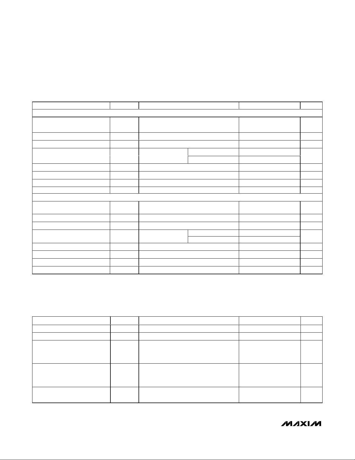
AC ELECTRICAL CHARACTERISTICS—OUTA AND OUTB (continued)
(Typical Application Circuit, VCC= +2.7V to +3.3V, R1= R2= R3= 0Ω, TA= -40°C to +85°C, unless otherwise noted. Typical values
are at V
CC
= 3.3V, CSETL = CSETH = VCC, TA= +25°C, unless otherwise noted.) (Note 1)
AC ELECTRICAL CHARACTERISTICS—OUTD
(Typical Application Circuit, VCC= +2.7V to +3.3V, R1= R2= R3= 0Ω, TA= -40°C to +85°C, unless otherwise noted. Typical values
are at V
CC
= 3.3V, CSETL = CSETH = VCC, TA= +25°C, unless otherwise noted.) (Note 1)
RSSI MODE—2.17GHz
RF Input Power Range (Note 2)
±3dB Dynamic Range TA = -20°C to +85°C (Note 3) 64 dB
Range Center -25 dBm
Temperature Sensitivity
Slope (Note 4) 17.8 mV/dB
Typical Slope Variation TA = -20°C to +85°C -8 µV/°C
Intercept (Note 5) -81 dBm
Typical Intercept Variation TA = -20°C to +85°C 0.03 dBm/°C
RSSI MODE—2.5GHz
RF Input Power Range (Note 2)
±3dB Dynamic Range TA = -20°C to +85°C (Note 3) 52 dB
Range Center -23 dBm
Temperature Sensitivity
Slope (Note 4) 17.8 mV/dB
Typical Slope Variation TA = -20°C to +85°C -8 µV/°C
Intercept (Note 5) -80 dBm
Typical Intercept Variation TA = -20°C to +85°C 0.03 dBm/°C
PARAMETER SYMBOL CONDITIONS MIN TYP MAX UNITS
-52 to
+12
P
RFINA
-25dBm
P
RFINA
-23dBm
= P
= P
RFINB
RFINB
TA = +25°C to +85°C +0.0135
=
= +25°C to -20°C -0.0135
T
A
TA = +25°C to +85°C +0.0167
=
= +25°C to -20°C -0.0167
T
A
-45 to
+7
dB/°C
dB/°C
dBm
dBm
OUTD Center Point P
Small-Signal Envelope Bandwidth No external capacitor on pins FV1 and FV2 22 MHz
Small-Signal Settling Time
Large-Signal Settling Time
Small-Signal Rise and Fall Time
PARAMETER SYMBOL CONDITIONS MIN TYP MAX UNITS
= P
RFINA
Any 8dB change on the inputs,
no external capacitor on FV1 and FV2,
settling accuracy is ±0.5dB
Any 30dB change on the inputs, no external
capacitor on pins FV1 and FV2, settling
accuracy is ±0.5dB
Any 8dB step, no external capacitor on pins
FV1 and FV2
RFINB
1V
150 ns
300 ns
15 ns
Page 5
MAX2016
LF-to-2.5GHz Dual Logarithmic Detector/
Controller for Power, Gain, and VSWR Measurements
_______________________________________________________________________________________ 5
AC ELECTRICAL CHARACTERISTICS—OUTD (continued)
(Typical Application Circuit, VCC= +2.7V to +3.3V, R1= R2= R3= 0Ω, TA= -40°C to +85°C, unless otherwise noted. Typical values
are at V
CC
= 3.3V, CSETL = CSETH = VCC, TA= +25°C, unless otherwise noted.) (Note 1)
Note 1: The MAX2016 is tested at T
A
= +25°C and is guaranteed by design for TA= -40°C to +85°C.
Note 2: Typical minimum and maximum range of the detector at the stated frequency.
Note 3: Dynamic range refers to the range over which the error remains within the ±3dB range.
Note 4: The slope is the variation of the output voltage per change in input power. It is calculated by fitting a root-mean-square
straight line to the data indicated by the RF input power range.
Note 5: The intercept is an extrapolated value that corresponds to the output power for which the output voltage is zero. It is calcu-
lated by fitting a root-mean-square straight line to the data.
Large-Signal Rise and Fall Time
±1dB Dynamic Range
Slope fRF = 0.1GHz to 2.5GHz (A-B) -25 mV/dB
OUTD Voltage Deviation
±1dB Dynamic Range over
Temperature Relative to Best-Fit
Curve at +25°C
Gain Measurement Balance
Channel Isolation
PARAMETER SYMBOL CONDITIONS MIN TYP MAX UNITS
Any 30dB step, no external capacitor on
pins FV1 and FV2
0.1GHz P
0.9GHz P
1.9GHz P
2.17GHz P
2.5GHz P
P
= P
RFINA
-20°C to +85°C
P
is swept ;
RFINA
= -20°C to
T
A
+85°C
= P
P
RFINB
1.9GHz
0.9GHz 90
1.9GHz 65
2.5GHz 55
= -30dBm, TA =
RFINB
= -50dBm to -5dBm, fRF =
RFINB
= -32dBm 80
RFINB
= -30dBm 75
RFINB
= -27dBm 60
RFINB
= -25dBm 55
RFINB
= -23dBm 50
RFINB
0.1GHz, P
-32dBm
0.9GHz, P
-30dBm
1.9GHz, P
-27dBm
2.17GHz, P
-25dBm
2.5GHz, P
-23dBm
RFINB
RFINB
RFINB
RFINB
RFINB
=
=
=
=
=
35 ns
±0.25 dB
80
70
55
50
45
0.2 dB
dB
dB
dB
Page 6
MAX2016
LF-to-2.5GHz Dual Logarithmic Detector/
Controller for Power, Gain, and VSWR Measurements
6 _______________________________________________________________________________________
Typical Operating Characteristics
(MAX2016 EV kit, VCC= 3.3V, R1= R2= R3= 0Ω, CSETL = CSETH = VCC, TA= +25°C, unless otherwise noted.)
DIFFERENTIAL OUTPUT VOLTAGE
vs. A/B DIFFERENCE
MAX2016 toc01
MAGNITUDE RATIO (dB)
V
OUTD
(V)
3010-10-30
0.5
1.0
1.5
2.0
2.5
0
-50 50
fIN = 100MHz
P
RFINB
= -32dBm P
RFINA
IS SWEPT
TA = -20°C,
+25°C, +85°C
DIFFERENTIAL OUTPUT-VOLTAGE ERROR
vs. A/B DIFFERENCE
MAX2016 toc02
MAGNITUDE RATIO (dB)
ERROR (dB)
3010-10-30
-2
-1
0
1
2
3
-3
-50 50
fIN = 100MHz
P
RFINB
= -32dBm
NORMALIZED TO DATA
AT +25°C
TA = -20°C
TA = +85°C
DIFFERENTIAL OUTPUT VOLTAGE
vs. A/B DIFFERENCE
MAX2016 toc03
MAGNITUDE RATIO (dB)
V
OUTD
(V)
3010-10-30
0.5
1.0
1.5
2.0
2.5
0
-50 50
fIN = 900MHz
P
RFINB
= -30dBm P
RFINA
IS SWEPT
TA = -20°C,
+25°C, +85°C
DIFFERENTIAL OUTPUT-VOLTAGE ERROR
vs. A/B DIFFERENCE
MAX2016 toc04
MAGNITUDE RATIO (dB)
ERROR (dB)
3010-10-30
-2
-1
0
1
2
3
-3
-50 50
fIN = 900MHz
P
RFINB
= -30dBm
NORMALIZED TO DATA
AT +25°C
TA = -20°C
TA = +85°C
DIFFERENTIAL OUTPUT VOLTAGE
vs. A/B DIFFERENCE
MAX2016 toc05
MAGNITUDE RATIO (dB)
V
OUTD
(V)
200-20
0.5
1.0
1.5
2.0
2.5
0
-40 40
fIN = 1900MHz
P
RFINB
= -27dBm
P
RFINA
IS SWEPT
TA = -20°C
TA = +25°C
TA = +85°C
DIFFERENTIAL OUTPUT-VOLTAGE ERROR
vs. A/B DIFFERENCE
MAX2016 toc06
MAGNITUDE RATIO (dB)
ERROR (dB)
200-20
-2
-1
0
1
2
3
-3
-40 40
fIN = 1900MHz
P
RFINB
= -27dBm
NORMALIZED TO DATA
AT +25°C
TA = -20°C
TA = +85°C
Page 7

MAX2016
LF-to-2.5GHz Dual Logarithmic Detector/
Controller for Power, Gain, and VSWR Measurements
_______________________________________________________________________________________ 7
Typical Operating Characteristics (continued)
(MAX2016 EV kit, VCC= 3.3V, R1= R2= R3= 0Ω, CSETL = CSETH = VCC, TA= +25°C, unless otherwise noted.)
(V)
OUTD
V
(V)
OUTD
V
DIFFERENTIAL OUTPUT VOLTAGE
vs. A/B DIFFERENCE
2.5
fIN = 2170MHz
= -25dBm P
P
RFINB
2.0
1.5
TA = +25°C
1.0
0.5
0
RFINA
TA = -20°C
TA = +85°C
MAGNITUDE RATIO (dB)
DIFFERENTIAL OUTPUT VOLTAGE
vs. A/B DIFFERENCE
2.5
fIN = 2500MHz
= -23dBm P
P
RFINB
2.0
1.5
TA = +85°C
1.0
0.5
RFINA
TA = -20°C
TA = +25°C
IS SWEPT
MAX2016 toc07
15-5-25-45 35
IS SWEPT
MAX2016 toc09
DIFFERENTIAL OUTPUT-VOLTAGE ERROR
vs. A/B DIFFERENCE
3
fIN = 2170MHz
= -25dBm
P
2
1
0
ERROR (dB)
-1
-2
-3
RFINB
NORMALIZED TO DATA
AT +25°C
TA = -20°C
TA = +85°C
-40 40
MAGNITUDE RATIO (dB)
DIFFERENTIAL OUTPUT-VOLTAGE ERROR
vs. A/B DIFFERENCE
3
fIN = 2500MHz
= -23dBm
P
2
1
0
ERROR (dB)
-1
-2
RFINB
NORMALIZED TO DATA
AT +25°C
TA = -20°C
TA = +85°C
200-20
MAX2016 toc08
MAX2016 toc10
0
MAGNITUDE RATIO (dB)
200-20-40 40
DIFFERENTIAL OUTPUT-VOLTAGE BALANCE
1.15
fIN = 1900MHz
1.10
1.05
(V)
1.00
OUTD
V
0.95
0.90
0.85
-60 0
TA = +25°C
TA = +85°C
TA = +25°C
TA = -20°C
TA = +85°C
TA = +25°C
TA = -20°C
P
RFINA
TA = +85°C
P
RFINA
P
P
= P
RFINA
(dBm)
= P
RFINA
RFINB
RFINB
-15-30-45
TA = -20°C
+ 5dB
= P
RFINB
- 5dB
MAX2016 toc11
-3
-40 40
MAGNITUDE RATIO (dB)
200-20
S11 MAGNITUDE
-10
-15
-20
-25
TA = +85°C
-30
-35
-40
MAGNITUDE (dB)
-45
-50
-55
-60
03.0
TA = +25°C
FREQUENCY (GHz)
TA = -20°C
2.52.01.51.00.5
MAX2016 toc12
Page 8
MAX2016
LF-to-2.5GHz Dual Logarithmic Detector/
Controller for Power, Gain, and VSWR Measurements
8 _______________________________________________________________________________________
Typical Operating Characteristics (continued)
(MAX2016 EV kit, VCC= 3.3V, R1= R2= R3= 0Ω, CSETL = CSETH = VCC, TA= +25°C, unless otherwise noted.)
V
OUTA
vs. P
RFINA
MAX2016 toc17
P
RFINA
(dBm)
V
OUTA
(V)
-5-25-45
0.5
1.0
1.5
2.0
2.5
0
-65 15
fIN = 1900MHz
TA = -20°C
TA = +25°C
TA = +85°C
V
OUTA
ERROR vs. P
RFINA
MAX2016 toc18
P
RFINA
(dBm)
ERROR (dB)
-5-25-45
-2
-1
0
1
2
3
-3
-65 15
fIN = 1900MHz
NORMALIZED TO DATA
AT +25°C
TA = -20°C
TA = +85°C
V
OUTA
vs. P
RFINA
MAX2016 toc13
P
RFINA
(dBm)
V
OUTA
(V)
0-20-40-60
0.5
1.0
1.5
2.0
2.5
0
-80 20
fIN = 100MHz
TA = -20°C
TA = +25°C
TA = +85°C
V
OUTA
ERROR vs. P
RFINA
MAX2016 toc14
P
RFINA
(dBm)
ERROR (dB)
0-20-40-60
-2
-1
0
1
2
3
-3
-80 20
fIN = 100MHz
NORMALIZED TO DATA
AT +25°C
TA = -20°C
TA = +85°C
V
OUTA
vs. P
RFINA
MAX2016 toc15
P
RFINA
(dBm)
V
OUTA
(V)
0-20-40-60
0.5
1.0
1.5
2.0
2.5
0
-80 20
fIN = 900MHz
TA = -20°C
TA = +25°C
TA = +85°C
V
OUTA
ERROR vs. P
RFINA
MAX2016 toc16
P
RFINA
(dBm)
ERROR (dB)
0-15-30-45-60
-2
-1
0
1
2
3
-3
-75 15
fIN = 900MHz
NORMALIZED TO DATA
AT +25°C
TA = -20°C
TA = +85°C
Page 9

MAX2016
LF-to-2.5GHz Dual Logarithmic Detector/
Controller for Power, Gain, and VSWR Measurements
_______________________________________________________________________________________ 9
Typical Operating Characteristics (continued)
(MAX2016 EV kit, VCC= 3.3V, R1= R2= R3= 0Ω, CSETL = CSETH = VCC, TA= +25°C, unless otherwise noted.)
V
OUTA
vs. P
RFINA
MAX2016 toc19
P
RFINA
(dBm)
V
OUTA
(V)
0-15-30-45
0.5
1.0
1.5
2.0
2.5
0
-60 15
fIN = 2170MHz
TA = -20°C
TA = +25°C
TA = +85°C
V
OUTA
ERROR vs. P
RFINA
MAX2016 toc20
P
RFINA
(dBm)
ERROR (dB)
0-15-30-45
-2
-1
0
1
2
3
-3
-60 15
fIN = 2170MHz
NORMALIZED TO DATA
AT +25°C
TA = -20°C
TA = +85°C
MAX2016 toc21
0-15-30-45
0.5
1.0
1.5
2.0
2.5
0
-60 15
V
OUTA
vs. P
RFINA
P
RFINA
(dBm)
V
OUTA
(V)
fIN = 2500MHz
TA = -20°C
TA = +25°C
TA = +85°C
-2
-1
0
1
2
3
-3
MAX2016 toc22
0-15-30-45-60 15
V
OUTA
ERROR vs. P
RFINA
P
RFINA
(dBm)
ERROR (dB)
fIN = 2500MHz
NORMALIZED TO DATA
AT +25°C
TA = -20°C
TA = +85°C
Page 10

MAX2016
LF-to-2.5GHz Dual Logarithmic Detector/
Controller for Power, Gain, and VSWR Measurements
10 ______________________________________________________________________________________
Detailed Description
The MAX2016 dual logarithmic amplifier is designed for
a multitude of applications including dual-channel RF
power measurements, AGC control, gain/loss detection,
and VSWR monitoring. This device measures RF signals
ranging from low frequency to 2.5GHz, and operates
from a single 2.7V to 5.25V (using series resistor, R6)
power supply. As with its single-channel counterpart
(MAX2015), the MAX2016 provides unparalleled performance with a high 80dB dynamic range at 100MHz and
exceptional accuracy over the extended temperature
and supply voltage ranges.
The MAX2016 uses a pair of logarithmic amplifiers to
detect and compare the power levels of two RF input
signals. The device subtracts one power level from the
other to provide a DC output voltage that is proportional
to the power difference (gain). The MAX2016 can also
measure the return loss/VSWR of an RF signal by monitoring the incident and reflected power levels associated with any given load.
A window detector is easily implemented by using the
on-chip comparators, OR gate, and 2V reference. This
combination of circuitry provides an automatic indication of when the measured gain is outside a programmable range. Alarm monitoring can thus be implemented for detecting high-VSWR states (such as open
or shorted loads).
RF Inputs (RFINA and RFINB)
The MAX2016 has two differential RF inputs. The input
to detector A (RFINA) uses the two input ports RFINA+
and RFINA-, and the input to detector B (RFINB) uses
the two input ports RFINB+ and RFINB-.
Pin Description
PIN NAME FUNCTION
1, 28 FA1, FA2
2, 9, 12, 20 V
3, 4 RFINA+, RFINA- Differential RF Inputs for Detector A. Requires external DC-blocking capacitors.
5, 17 GND Ground. Connect to the PCB ground plane.
6 COUTH High-Comparator Output
7 CSETH Threshold Input on High Comparator
8 COR Comparator OR Logic Output. Output of COUTH ORed with COUTL.
10 SETD Set-Point Input for Gain Detector
11 OUTD
13, 14 FV2, FV1 Video-Filter Capacitor Inputs for OUTD
15 CSETL Threshold Set Input on Low Comparator
16 COUTL Low-Comparator Output
18, 19 RFINB-, RFINB+ Differential RF Inputs for Detector B. Requires external DC-blocking capacitors.
21, 22 FB1, FB2
23 OUTB
24 SETB Set-Point Input for Detector B
25 REF 2V Reference Output
26 SETA Set-Point Input for Detector A
27 OUTA
EP GND Exposed Paddle. EP must connect to the PCB ground plane.
CC
External Capacitor Input. Connecting a capacitor between FA1 and FA2 sets the highpass cutoff
frequency corner for detector A (see the Input Highpass Filter section).
Supply Voltage. Bypass with capacitors as specified in the Typical Application Circuit. Place
capacitors as close to each V
DC Output Voltage Representing P
proportional to the difference of the input RF powers on RFINA and RFINB.
External Capacitor Input. Connecting a capacitor between FB1 and FB2 sets the highpass cutoff
frequency corner for detector B (see the Input Highpass Filter section).
Detector B Output. This output provides a voltage proportional to the log of the input power on
differential inputs RFINB+ and RFINB- (RFINB).
Detector A Output. This output provides a voltage proportional to the log of the input power on
differential inputs RFINA+ and RFINA- (RFINA).
as possible (see the Power-Supply Connections section).
CC
RFINA
- P
. This output provides a DC voltage
RFINB
Page 11

MAX2016
LF-to-2.5GHz Dual Logarithmic Detector/
Controller for Power, Gain, and VSWR Measurements
______________________________________________________________________________________ 11
The differential RF inputs allow for the measurement of
broadband signals ranging from low frequency to
2.5GHz. For single-ended signals, RFINA- and RFINBare AC-coupled to ground. The RF inputs are internally
biased and need to be AC-coupled. Using 680pF
capacitors, as shown in the Typical Application Circuit,
results in a 10MHz highpass corner frequency. An
internal 50Ω resistor between RFINA+ and RFINA- (as
well as RFINB+ and RFINB-) produces a good low-frequency to 3.0GHz match.
SETA, SETB, and SETD Inputs
The SET_ inputs are used for loop control when the
device is in controller mode. Likewise, these same
SET_ inputs are used to set the slope of the output signal (mV/dB) when the MAX2016 is in detector mode.
The center node of the internal resistor-divider is fed to
the negative input of the power detector’s internal output op amp.
Reference
The MAX2016 has an on-chip 2V voltage reference.
The internal reference output is connected to REF. The
output can be used as a reference voltage source for
the comparators or other components and can source
up to 2mA.
OUTA and OUTB
Each OUT_ is a DC voltage proportional to the RF input
power level. The change of OUT_ with respect to the
power input is approximately 18mV/dB (R1= R2= 0Ω).
The input power level can be determined by the following
equation:
where P
INT
is the extrapolated intercept point of where
the output voltage intersects the horizontal axis.
OUTD
OUTD is a DC voltage proportional to the difference of
the input RF power levels. The change of the OUTD
with respect to the power difference is -25mV/dB (R3 =
0Ω). The difference of the input power levels (gain) can
be determined by the following equation:
where V
CENTER
is the output voltage, typically 1V, when
P
RFINA
= P
RFINB
.
Applications Information
Monitoring VSWR and Return Loss
The MAX2016 can be used to measure the VSWR of an
RF signal, which is useful for detecting the presence or
absence of a properly loaded termination, such as an
antenna (see Figure 1). The transmitted wave from the
power amplifier is coupled to RFINA and to the antenna. The reflected wave from the antenna is connected
to RFINB through a circulator. When the antenna is
missing or damaged, a mismatch in the nominal load
PP
VV
SLOPE
RFINA RFINB
OUTD CENTER
−
=
−()
P
V
SLOPE
P
RFIN
OUT
INT_
_
=+
Figure 1. VSWR Monitoring Configuation
TRANSMITTER
V
REF
LOGARITHMIC
RFINA
DETECTOR
LOGARITHMIC
RFINB
DETECTOR
COUPLER
CIRCULATOR
ATTENUATOR
MAX2016
20kΩ
CSETL
COUTL
OUTD
SETD
GND
COUTL
OUTD
Page 12

MAX2016
LF-to-2.5GHz Dual Logarithmic Detector/
Controller for Power, Gain, and VSWR Measurements
12 ______________________________________________________________________________________
impedance results, leading to an increase in reflected
power and subsequent change in the transmission
line’s VSWR. This increase in reflected power is manifested by an increase in the voltage at OUTD. An alarm
condition can be set by using the low comparator output (COUTL) as shown in Figure 1. The comparator
automatically senses the change in VSWR, yielding a
logic 0 as it compares OUTD to a low DC voltage at
CSETL. CSETL, in turn, is set by using the internal reference voltage and an external resistor-divider network.
For accurate measurement of signals carrying significant amplitude modulation, limit the bandwidth of the
difference amplifier to be less than the lowest modulation frequency. This will minimize the ripple in the
OUTD waveform. This is particularly appropriate if the
system-level time delay between the two sense points
is significant with respect to the period of modulation.
Figure 1 illustrates a simple level detector. For windowdetector implementation, see the Comparator/Window
Detector section.
Measuring VSWR and Return Loss
In Figure 2, the two logarithmic amplifiers measure the
incident and the reflected power levels to produce two
proportional output voltages at OUTA and OUTB. Since
OUTD is a DC voltage proportional to the difference of
OUTA and OUTB, return loss (RL) and VSWR can be
easily calculated within a microprocessor using the
following relationships:
where return loss (RL) is expressed in decibels,
V
CENTER
is the output voltage (typically 1V) when
P
RFINA
= P
RFINB
, and SLOPE is typically equal to
-25mV/dB (for R3 = 0Ω).
VSWR can similarly be calculated through the following
relationship:
Figure 2. Measuring Return Loss and VSWR of a Given Load
LOGARITHMIC
RFINA
RFINB
DETECTOR
LOGARITHMIC
DETECTOR
RL P P
=− =
RFINA RFINB
VV
()
−
OUTD CENTER
SLOPE
RL
⎛⎝⎞
−
⎠
20
+
RL
⎛⎝⎞
−
⎠
20
−
μ
P
OUTD
SETD
VSWR
=
ADC
110
110
MAX2016
IN
4-PORT DIRECTIONAL
COUPLER
LOAD
20k
Ω
GND
Page 13

MAX2016
LF-to-2.5GHz Dual Logarithmic Detector/
Controller for Power, Gain, and VSWR Measurements
______________________________________________________________________________________ 13
Measuring Gain
The MAX2016 can be used to measure the gain of an
RF block (or combination of blocks) through the implementation outlined in Figure 3. As shown, a coupled
signal from the input of the block is fed into RFINA,
while the coupled output is connected to RFINB. The
DC output voltage at OUTD is proportional to the power
difference (i.e., gain).
The gain of a complete receiver or transmitter lineup
can likewise be measured since the MAX2016 accepts
RF signals that range from low frequency to 2.5GHz;
see Figure 4. The MAX2016 accurately measures the
gain, regardless of the different frequencies present
within superheterodyne architectures.
For accurate measurement of signals carrying significant amplitude modulation, limit the bandwidth of the
difference amplifier to be less than the lowest modulation frequency. This will minimize the ripple in the
OUTD waveform. This is particularly appropriate if the
system-level time delay between the two sense points
is significant with respect to the period of modulation.
Figure 3. Gain Measurement Configuration
Figure 4. Conversion Gain Measurement Configuration
Ω
MAX2016
20k
SETD
LOGARITHMIC
COUPLER
IN
RFINA
RFINB
RF BLOCK
COUPLER
OUT
DETECTOR
LOGARITHMIC
DETECTOR
COUPLER
RFINA
f
RF
LOGARITHMIC
DETECTOR
MAX2016
OUTD
GND
LNA
20k
OUTD
MIXER
LO
LOGARITHMIC
DETECTOR
Ω
RFINB
OUTD
SETD
f
IF
COUPLER
OUT
Page 14
MAX2016
LF-to-2.5GHz Dual Logarithmic Detector/
Controller for Power, Gain, and VSWR Measurements
14 ______________________________________________________________________________________
Measuring Power (RSSI Detector Mode)
In detector mode, the MAX2016 acts like a receive-signal-strength indicator (RSSI), which provides an output
voltage proportional to the input power. This is accomplished by providing a feedback path from OUTA
(OUTB) to SETA (SETB) (R1/R2 = 0Ω; see Figure 5).
By connecting SET_ directly to OUT_, the op-amp gain
is set to 2V/V due to two internal 20kΩ feedback resistors. This provides a detector slope of approximately
18mV/dB with a 0.5V to 1.8V output range.
Gain-Controller Mode
The MAX2016 can be used as a gain controller within
an automatic gain-control (AGC) loop. As shown in
Figure 6, RFINA and RFINB monitor the VGA’s input
and output power levels, respectively. The MAX2016
produces a DC voltage at OUTD that is proportional to
the difference in these two RF input power levels. An
internal op amp compares the DC voltage with a reference voltage at SETD. The op amp increases or
decreases the voltage at OUTD until OUTD equals
SETD. Thus, the MAX2016 adjusts the gain of the VGA
to a level determined by the voltage applied to SETD.
Place the nominal signal levels of RFINA and RFINB
near the middle of their respective dynamic ranges to
accommodate the largest range of gain compensation.
This is nominally -25dBm to -30dBm. If so selected, the
nominal voltage applied to SETD will be approximately
1.0V. Operate the SETD voltage within the range of
0.5V to 1.5V for the greatest accuracy of gain control.
Figure 5. In Detector Mode (RSSI), OUTA/OUTB is a DC
Voltage Proportional to the Input Power
Figure 6. In Gain-Controller Mode, the OUTD Maintains the
Gain of the VGA
IN_
RFIN+A
RFIN-A
GND
DETECTORS
20k
Ω
20k
OUTA
SETA
R1/R2
Ω
OUTA
VGA
VGA INPUT
COUPLER
SET-POINT
DAC
GAIN CONTROL INPUT
OUTDSETD
VGA OUTPUT
COUPLER
MAX2016
DETECTORS
IN_
RFIN+B
RFIN-B
20k
Ω
20k
OUTB
SETB
R1/R2
Ω
OUTB
Ω
20k
RFINA
LOGARITHMIC
DETECTOR
MAX2016
LOGARITHMIC
DETECTOR
RFINB
Page 15

MAX2016
LF-to-2.5GHz Dual Logarithmic Detector/
Controller for Power, Gain, and VSWR Measurements
______________________________________________________________________________________ 15
Power-Controller Mode
The MAX2016 can also be used as a power detector/
controller within an AGC loop. Figure 7 depicts a scenario where the MAX2016 is employed as the AGC circuit. As shown in the figure, the MAX2016 monitors the
output of the PA through a directional coupler. An internal differencing amplifier (Figure 5) compares the
detected signal with a reference voltage determined by
V
SET_
. The differencing amplifier increases or decreases the voltage at OUT_, according to how closely the
detected signal level matches the V
SET_
reference. The
MAX2016 maintains the power of the PA to a level
determined by the voltage applied to SET_.
Since the logarithmic detector responds to any amplitude modulation being carried by the carrier signal, it
may be necessary to insert an external lowpass filter
between the differencing amplifier output
(OUTA/OUTB) and the gain-control element to remove
this modulation signal.
OUTA and OUTB Slope Adjustment
The transfer slope function of OUTA and OUTB can be
increased from its nominal value by varying resistors
R1 and R2 (see the Typical Application Circuit). The
equation controlling the slope is:
OUTD Slope Adjustment
The transfer slope function of OUTD can be increased
from its nominal value by varying resistor R3 (see the
Typical Application Circuit). The equation controlling
the slope is:
Input Highpass Filters
The MAX2016 integrates a programmable highpass filter on each RF input. The lower cutoff frequency of the
MAX2016 can be decreased by increasing the external
capacitor value between FA1 and FA2 or FB1 and FB2.
By default, with no capacitor connecting FA1 and FA2
or FB1 and FB2, the lower cutoff frequency is 20MHz.
Using the following equation determines the lowest
operating frequency:
where R = 2Ω.
Differential Output Video Filter
The bandwidth and response time difference of the output amplifier can be controlled with the external capacitor, C15, connected between FV1 and FV2. With no
external capacitor, the bandwidth is greater than 20MHz.
The following equation determines the bandwidth of the
amplifier difference:
where R = 1.8kΩ.
Use a video bandwidth lower than the anticipated lowest amplitude-modulation frequency range to yield the
greatest accuracy in tracking the average carrier
power for high peak-to-average ratio waveforms.
Figure 7. In Power-Controller Mode, the DC Voltage at OUTA or
OUTB Controls the Gain of the PA, Leading to a Constant
Output Power Level (Note: Only one controller channel is
shown within the figure. Since the MAX2016 is a dual controller/detector, the second channel can be easily implemented
by using the adjacent set of input and output connections.)
POWER AMPLIFIER
TRANSMITTER
LOWPASS
FILTER
GAIN-CONTROL INPUT
OUTA/
OUTB
LOGARITHMIC
DETECTOR
RFINA/
RFINB
COUPLER
SLOPE OUTA OR OUTB
=
⎜
⎝
dB
⎢
⎟
⎠
20
⎢
⎣
⎡
1240
RorR k
()
mV
⎛
⎞
9
⎤
+
⎥
k
⎥
⎦
SLOPE OUTD
⎛
=−
⎜
⎝
mVdBRk
25
⎞
⎟
⎠
320
⎛
⎜
⎝
20
+
⎞
⎟
⎠
k
frequencyRC=
1
2π
SETA/
SET-POINT
DAC
SETB
20kΩ
20kΩ
MAX2016
frequencyRC=
1
2π
Page 16

MAX2016
LF-to-2.5GHz Dual Logarithmic Detector/
Controller for Power, Gain, and VSWR Measurements
16 ______________________________________________________________________________________
Comparators/Window Detectors
The MAX2016 integrates two comparators for use in
monitoring the difference in power levels (gain) of
RFINA and RFINB. The thresholds of the two comparators are set to the voltage applied to the CSETL and
CSETH pins. The output of each comparator can be
monitored independently or from the COR output that
ORs the outputs of the individual comparators. This can
be used for a window-detector function.
These comparators can be used to trigger hardware
interrupts, allowing rapid detection of over-range conditions. These comparators are high-speed devices.
Connect high-value bypass capacitors (0.1µF) between
each comparator threshold input (CSETL and CSETH)
to ground to provide a solid threshold voltage at high
switching speeds.
Some applications may benefit from the use of hysteresis in the comparator response. This can be useful for
prevention of false triggering in the presence of small
noise perturbations in the signal levels, or with signals
with large amplitude modulation. To introduce hysteresis
into the comparator output, connect a feedback resistor
from COUTL to CSTEL. Select the value of this resistor,
in combination with the resistive-divider values used to
set threshold-level CSETL, to set the amount of hysteresis. Set the parallel combination of resistors connected
to CSETL to be less than 10kΩ for best performance.
Figure 8 illustrates the use of these comparators in a
gain-monitoring application. The low comparator has its
threshold (CSETL) set at a low-gain trip point. If the
gain drops below this trip point, the COUTL output
goes from a logic 0 to a logic 1. The high comparator
has its threshold (CSETH) set at a high trip point. If the
gain exceeds this trip point, the COUTH output goes
from logic 0 to logic 1. The window comparator output
(COR) rests a logic 0 if the gain is in the acceptable
range, between CSETL and CSETH. It goes to a logic 1
if the gain is either above or below these limits.
Power-Supply Connection
The MAX2016 is designed to operate from a single
+2.7V to +3.6V supply. To operate under a higher supply voltage range, a resistor must be connected in series
with the power supply and VCCto reduce the voltage
delivered to the chip. For a +4.75V to +5.25V supply,
use a 37.4Ω (±1%) resistor in series with the supply.
Layout Considerations
A properly designed PCB is an essential part of any
RF/microwave circuit. Keep RF signal lines as short as
possible to reduce losses, radiation, and inductance.
For the best performance, route the ground pin traces
directly to the exposed pad under the package. The
PCB exposed pad MUST be connected to the ground
plane of the PCB. It is suggested that multiple vias be
used to connect this pad to the lower level ground
Figure 8. Window Comparators Monitoring Mode. COR goes high if OUTD drops below CSETL or rises above CSETH.
CSETH
MAX2016
COR
LOGARITHMIC
RFINA
RFINB
DETECTOR
LOGARITHMIC
DETECTOR
CSETL
OUTD
Ω
20k
IN
RF BLOCK
COUPLER
OUT
COUPLER
SETD
Page 17

MAX2016
LF-to-2.5GHz Dual Logarithmic Detector/
Controller for Power, Gain, and VSWR Measurements
______________________________________________________________________________________ 17
Functional Diagram
planes. This method provides a good RF/thermal conduction path for the device. Solder the exposed pad on
the bottom of the device package to the PCB. The
MAX2016 Evaluation Kit can be used as a reference for
board layout. Gerber files are available upon request at
www.maxim-ic.com.
Power-Supply Bypassing
Proper voltage-supply bypassing is essential for highfrequency circuit stability. Bypass each V
CC
pin with a
capacitor as close to the pin as possible (Typical
Application Circuit).
Exposed Pad RF/Thermal Considerations
The exposed paddle (EP) of the MAX2016’s 28-pin thin
QFN-EP package provides two functions. One is a low
thermal-resistance path to the die; the second is a lowRF impedance ground connection. The EP MUST be
soldered to a ground plane on the PCB, either directly
or through an array of plated via holes (minimum of four
holes to provide ground integrity).
2, 9, 12, 20
5, 17
V
GND
CC
20k
Ω
20k
Ω
REFSETA OUTA OUTB SETB
2.0V
REF
2423252726
20k
Ω
20k
Ω
3
RFINA+
67
LOG
AMPLIFIERS
EXPOSED
PAD
16 15 11 10
CSETL
Ω
50
RFINA-
4
1
FA1
28
FA2
COR
8
SETDOUTDCSETH COUTH COUTL
LOG
AMPLIFIERS
20k
MAX2016
Ω
Ω
50
RFINB+
RFINB-
FB1
FB2
FV1
FV2
19
18
21
22
14
13
Page 18

MAX2016
LF-to-2.5GHz Dual Logarithmic Detector/
Controller for Power, Gain, and VSWR Measurements
18 ______________________________________________________________________________________
Typical Application Circuit
Chip Information
PROCESS: BiCMOS
Table 1. Component Values Used in the Typical Application Circuit
V
COMPARATORA
RFINA
V
OUTA
V
CC
C3
C4
C1
C2
V
CC
C16
A + B
1
2
3
4
5
6
7
FA1
V
CC
RFINA+
RFINA-
GND
COUTH
CSETH
V
CC
28
FA2
COR8V
27
OUTA
EXPOSED
CC
9
REF
R1
R2
26
25
REF
SETA
MAX2016
PADDLE
SETD10OUTD11V
24
SETB
CC
12
23
OUTB
FV213FV1
14
V
CC
22
FB2
FB1
V
RFINB+
RFINB-
GND
COUTL
CSETL
C15
V
OUTB
V
S
C10
C8
C9
C17
V
CC
C11
RFINB
COMPARATORB
V
CC
C12C5
21
20
CC
19
18
17
16
15
V
CC
R6
C18
C6
NOTE:
COMPARATORS ARE DISABLED
BY CONNECTING CSETL AND CSETH TO V
C7
R3
.
CC
C13
V
C14
OUTD
DESIGNATION VALUE DESCRIPTION
C1, C2, C8, C9 680pF Microwave capacitors (0402)
C3, C6, C10, C13 33pF Microwave capacitors (0402)
C4, C7, C11, C14 0.1µF Microwave capacitors (0603)
C5, C12, C15, C16, C17 Not used Capacitors are optional for frequency compensation, bypass
C18 10µF Tantalum capacitor (C case)
R1, R2, R3 0Ω Resistors (0402)
R6
0Ω Resistor (1206) for VS = 2.7V to 3.6V
37.4Ω ±1% resistor (1206) for V
= 4.75V to 5.25V
S
Page 19

MAX2016
LF-to-2.5GHz Dual Logarithmic Detector/
Controller for Power, Gain, and VSWR Measurements
______________________________________________________________________________________ 19
Package Information
(The package drawing(s) in this data sheet may not reflect the most current specifications. For the latest package outline information,
go to www.maxim-ic.com/packages
.)
QFN THIN.EPS
Page 20

MAX2016
LF-to-2.5GHz Dual Logarithmic Detector/
Controller for Power, Gain, and VSWR Measurements
Maxim cannot assume responsibility for use of any circuitry other than circuitry entirely embodied in a Maxim product. No circuit patent licenses are
implied. Maxim reserves the right to change the circuitry and specifications without notice at any time.
20 ____________________Maxim Integrated Products, 120 San Gabriel Drive, Sunnyvale, CA 94086 408-737-7600
© 2006 Maxim Integrated Products is a registered trademark of Maxim Integrated Products, Inc.
MAX2016MAX2016
Package Information (continued)
(The package drawing(s) in this data sheet may not reflect the most current specifications. For the latest package outline information,
go to www.maxim-ic.com/packages
.)
Revision History
Pages changed at Rev 1: 1, 5, 10–20
 Loading...