

Page 1
General Description
The MAX2015 complete multistage logarithmic amplifier
is designed to accurately convert radio-frequency (RF)
signal power in the 0.1GHz to 3GHz frequency range to
an equivalent DC voltage. The outstanding dynamic
range and precision over temperature of this log amplifier make it particularly useful for a variety of base station and other wireless applications, including
automatic gain control (AGC), transmitter power measurements, and received signal strength indication
(RSSI) for terminal devices.
The MAX2015 can also be operated in a controller
mode where it measures, compares, and controls the
output power of a variable-gain amplifier as part of a
fully integrated AGC loop.
This logarithmic amplifier provides much wider measurement range and superior accuracy compared to
controllers based on diode detectors, while achieving
excellent temperature stability over the full -40°C to
+85°C operating range.
Applications
AGC Measurement and Control
RF Transmitter Power Measurement
RSSI Measurements
Cellular Base Station, WLAN, Microwave Link,
Radar, and other Military Applications
Features
♦ Complete RF Detector/Controller
♦ 0.1GHz to 3GHz Frequency Range
♦ Exceptional Accuracy Over Temperature
♦ High Dynamic Range
♦ 2.7V to 5.25V Supply Voltage Range*
♦ Scaling Stable Over Supply and Temperature
Variations
♦ Controller Mode with Error Output
♦ Shutdown Mode with Typically 1µA of Supply
Current
♦ Available in 8-Pin µMAX
®
and TDFN Packages
MAX2015
0.1GHz to 3GHz, 75dB Logarithmic
Detector/Controller
________________________________________________________________ Maxim Integrated Products 1
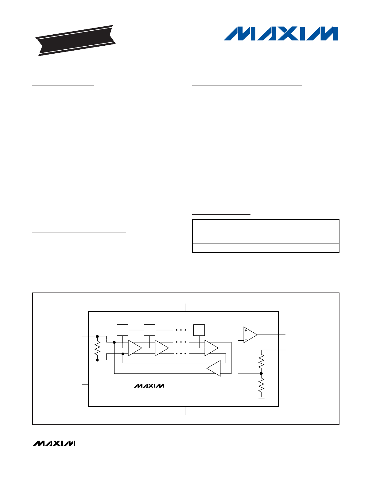
Ordering Information
MAX2015
7dB
Σ
50Ω
20kΩ
SET
OUT
8
7
2
INHI
INLO
3
6
1, 4
PWDN
5
20kΩ
Σ
7dB
Σ
7dB
V
CC
GND
POWER DETECTORS
OFFSET AND COMMON-
MODE AMP
Functional Diagram
19-2998; Rev 2; 2/07
For pricing, delivery, and ordering information, please contact Maxim/Dallas Direct! at
1-888-629-4642, or visit Maxim’s website at www.maxim-ic.com.
EVALUATION KIT
AVAILABLE
Pin Configuration appears at end of data sheet.
PART
TEMP RANGE
PIN-
PKG
CODE
MAX2015EUA
8 µMAX
U8-1
MAX2015EUA-T
8 µMAX
U8-1
*See Power-Supply Connections section.
µMAX is a registered trademark of Maxim Integrated Products, Inc.
T = Tape-and-reel.
+Denotes lead-free and RoHS compliance.
*EP = Exposed paddle.
Ordering Information continued at end of data sheet.
PACKAGE
-40°C to +85°C
-40°C to +85°C
Page 2
MAX2015
0.1GHz to 3GHz, 75dB Logarithmic
Detector/Controller
2 _______________________________________________________________________________________
ABSOLUTE MAXIMUM RATINGS
DC ELECTRICAL CHARACTERISTICS
(MAX2015 typical application circuit (Figure 1), VS= +3.3V, fRF= 100MHz to 3000MHz, R1 = 0Ω, R4 = 0Ω, RL= 10kΩ, TA= -40°C to
+85°C, unless otherwise noted. Typical values are at T
A
= +25°C, unless otherwise noted.) (Note 1)
Stresses beyond those listed under “Absolute Maximum Ratings” may cause permanent damage to the device. These are stress ratings only, and functional
operation of the device at these or any other conditions beyond those indicated in the operational sections of the specifications is not implied. Exposure to
absolute maximum rating conditions for extended periods may affect device reliability.
VCC(Pins, 1, 4) to GND.......................................-0.3V to +5.25V
SET, PWDN to GND....................................-0.3V to (V
CC
+ 0.3V)
Input Power Differential INHI, INLO................................+23dBm
Input Power Single Ended (INHI or INLO grounded).....+19dBm
Continuous Power Dissipation (T
A
= +70°C)
8-Pin µMAX (derate 4.5mW/°C above +70°C) .............362mW
8-Pin TDFN (derate 18.5mW/°C above +70°C) .........1480mW
Operating Temperature Range ...........................-40°C to +85°C
Junction Temperature......................................................+150°C
Storage Temperature Range .............................-65°C to +150°C
Lead Temperature (soldering, 10s) .................................+300°C
PARAMETER
SYMBOL
CONDITIONS MIN TYP MAX UNITS
POWER SUPPLY
R4 = 75Ω ±1%, PWDN must be
connected to GND
4.75 5.25
Supply Voltage V
S
R4 = 0Ω 2.7 3.6
V
TA = +25°C, VS = 5.25V,
R4 = 75Ω
17.3
Supply Current I
CC
TA = +25°C 17.3 20.5
mA
I
CC
TA = -40°C to +85°C 0.05 mA/°C
Shutdown Current I
CC
V
PWDN
= V
CC
1µA
CONTROLLER REFERENCE (SET)
SET Input Voltage Range
V
SET Input Impedance 40 kΩ
DETECTOR OUTPUT (OUT)
Source Current 4mA
Sink Current 450 µA
Minimum Output Voltage
)
0.5 V
Maximum Output Voltage
)
1.8 V
Supply Current Variation with Temp
0.5 to 1.8
V
OUT(MIN
V
OUT(MAX
Page 3
MAX2015
0.1GHz to 3GHz, 75dB Logarithmic
Detector/Controller
_______________________________________________________________________________________ 3
AC ELECTRICAL CHARACTERISTICS
(MAX2015 typical application circuit (Figure 1), VS= +3.3V, fRF= 100MHz to 3000MHz, R1 = 0Ω, R4 = 0Ω, RL= 10kΩ, TA= -40°C to
+85°C, unless otherwise noted. Typical values are at T
A
= +25°C, unless otherwise noted.) (Note 1)
PARAMETER
CONDITIONS MIN TYP MAX
UNITS
RF Input Frequency Range f
RF
GHz
Return Loss S
11
-15 dB
Large-Signal Response Time
P
IN
= no signal to 0dBm,
±0.5dB settling accuracy
150 ns
RSSI MODE—0.1GHz
RF Input Power Range (Note 2)
dBm
±3dB Dynamic Range TA = -40°C to +85°C (Note 3) 70 dB
Range Center -30 dBm
Temp Sensitivity when TA > +25°C
T
A
= +25°C to +85°C,
P
IN
= -25dBm
dB/°C
Temp Sensitivity when TA < +25°C
T
A
= -40°C to +25°C,
P
IN
= -25dBm
dB/°C
Slope (Note 4) 19
mV/dB
Typical Slope Variation TA = -40°C to +85°C -4
µV/°C
Intercept (Note 5) -100 dBm
Typical Intercept Variation TA = -40°C to +85°C 0.03
dBm/°C
RSSI MODE—0.9GHz
RF Input Power Range (Note 2)
dBm
±3dB Dynamic Range TA = -40°C to +85°C (Note 3) 70 dB
Range Center -30 dBm
Temp Sensitivity when TA > +25°C
T
A
= +25°C to +85°C,
P
IN
= -25dBm
dB/°C
Temp Sensitivity when TA < +25°C
T
A
= -40°C to +25°C,
P
IN
= -25dBm
dB/°C
Slope (Note 4) 18.1
mV/dB
Typical Slope Variation TA = -40°C to +85°C -4
µV/°C
Intercept (Note 5) -97 dBm
Typical Intercept Variation TA = -40°C to +85°C 0.02
dBm/°C
RSSI MODE—1.9GHz
RF Input Power Range (Note 2)
dBm
±3dB Dynamic Range TA = -40°C to +85°C (Note 3) 60 dB
Range Center -25 dBm
Temp Sensitivity when TA > +25°C
T
A
= +25°C to +85°C,
P
IN
= -25dBm
dB/°C
Temp Sensitivity when TA < +25°C
T
A
= -40°C to +25°C,
P
IN
= -25dBm
dB/°C
Slope (Note 4) 18
mV/dB
Typical Slope Variation TA = -40°C to +85°C -4.8
µV/°C
SYMBOL
0.1 to 3
-65 to +5
+0.0083
-0.0154
-65 to +5
±0.0083
-0.0154
-55 to +5
±0.0033
-0.0138
Page 4
MAX2015
0.1GHz to 3GHz, 75dB Logarithmic
Detector/Controller
4 _______________________________________________________________________________________
PARAMETER
SYMBOL
CONDITIONS MIN TYP MAX
UNITS
Intercept (Note 5) -83 dBm
Typical Intercept Variation TA = -40°C to +85°C 0.03
dBm/°C
RSSI MODE—2.5GHz
RF Input Power Range (Note 2)
dBm
±3dB Dynamic Range TA = -40°C to +85°C (Note 3) 40 dB
Range Center -25 dBm
Temp Sensitivity when TA > +25°C
T
A
= +25°C to +85°C,
P
IN
= -25dBm
dB/°C
Temp Sensitivity when TA < +25°C
T
A
= -40°C to +25°C,
P
IN
= -25dBm
dB/°C
Slope (Note 4) 16.8
mV/dB
Typical Slope Variation TA = -40°C to +85°C -8
µV/°C
Intercept (Note 5) -81 dBm
Typical Intercept Variation TA = -40°C to +85°C 0.03
dBm/°C
Note 1: The MAX2015 is guaranteed by design for TA= -40°C to +85°C, as specified.
Note 2: Typical minimum and maximum range of the detector at the stated frequency.
Note 3: Dynamic range refers to the range over which the error remains within the stated bounds. The error is calculated at -40°C
and +85°C, relative to the curve at +25°C.
Note 4: The slope is the variation of the output voltage per change in input power. It is calculated by fitting a root-mean-square
(RMS) straight line to the data indicated by RF input power range.
Note 5: The intercept is an extrapolated value that corresponds to the output power for which the output voltage is zero.
It is calculated by fitting an RMS straight line to the data.
AC ELECTRICAL CHARACTERISTICS (continued)
(MAX2015 typical application circuit (Figure 1), VS= +3.3V, fRF= 100MHz to 3000MHz, R1 = 0Ω, R4 = 0Ω, RL= 10kΩ, TA= -40°C to
+85°C, unless otherwise noted. Typical values are at T
A
= +25°C, unless otherwise noted.) (Note 1)
-45 to -5
-0.0083
-0.0083
Page 5

MAX2015
0.1GHz to 3GHz, 75dB Logarithmic
Detector/Controller
_______________________________________________________________________________________ 5
OUTPUT VOLTAGE
vs. INPUT POWER
MAX2015 toc01
INPUT POWER (dBm)
OUTPUT VOLTAGE (V)
0-10-60 -50 -40 -30 -20
0.6
0.8
1.0
1.2
1.4
1.6
1.8
2.0
0.4
-70 10
fIN = 0.1GHz
TA = +85°C
TA = +25°C
TA = -40°C
OUTPUT-VOLTAGE ERROR
vs. INPUT POWER
MAX2015 toc02
INPUT POWER (dBm)
ERROR (dB)
0
-10-20-30-40-50-60
-2
-1
0
1
2
3
-3
-70
fIN = 0.1GHz
NORMALIZED TO DATA AT +25°C
TA = +85°C
TA = +25°C
TA = -40°C
OUTPUT-VOLTAGE ERROR
vs. INPUT POWER
MAX2015 toc03
INPUT POWER (dBm)
ERROR (dB)
0-10-20-30-40-50-60
-2
-1
0
1
2
3
-3
-70 10
VCC = 2.7V
VCC = 3.0V
VCC = 3.3V
VCC = 3.6V
fIN = 0.1GHz, TA = +85°C
NORMALIZED TO DATA AT +25°C
OUTPUT-VOLTAGE ERROR
vs. INPUT POWER
MAX2015 toc04
INPUT POWER (dBm)
ERROR (dB)
0-10-20-30-40-50-60
-2
-1
0
1
2
3
-3
-70 10
VCC = 3.3V
VCC = 3.6V
VCC = 2.7V
VCC = 3.0V
fIN = 0.1GHz, TA = -40°C
NORMALIZED TO DATA AT +25°C
OUTPUT VOLTAGE
vs. INPUT POWER
MAX2015 toc05
INPUT POWER (dBm)
OUTPUT VOLTAGE (V)
0-10-60 -50 -40 -30 -20
0.6
0.8
1.0
1.2
1.4
1.6
1.8
2.0
0.4
-70 10
fIN = 0.9GHz
TA = +85°C
TA = +25°C
TA = -40°C
OUTPUT-VOLTAGE ERROR
vs. INPUT POWER
MAX2015 toc06
INPUT POWER (dBm)
ERROR (dB)
0-10-20-30-40-50-60
-2
-1
0
1
2
3
-3
-70 10
fIN = 0.9GHz
NORMALIZED TO DATA AT +25°C
TA = +85°C
TA = +25°C
TA = -40°C
OUTPUT-VOLTAGE ERROR
vs. INPUT POWER
MAX2015 toc07
INPUT POWER (dBm)
ERROR (dB)
0-10-20-30-40-50-60
-2
-1
0
1
2
3
-3
-70 10
VCC = 3.0V
VCC = 3.3V
VCC = 3.6V
VCC = 2.7V
fIN = 0.9GHz, TA = +85°C
NORMALIZED TO DATA AT +25°C
OUTPUT-VOLTAGE ERROR
vs. INPUT POWER
MAX2015 toc08
INPUT POWER (dBm)
ERROR (dB)
0-10-20-30-40-50-60
-2
-1
0
1
2
3
-3
-70 10
VCC = 3.3V
VCC = 3.6V
VCC = 2.7V
VCC = 3.0V
fIN = 0.9GHz, TA = -40°C
NORMALIZED TO DATA AT +25°C
OUTPUT VOLTAGE
vs. INPUT POWER
MAX2015 toc09
INPUT POWER (dBm)
OUTPUT VOLTAGE (V)
0-10-60 -50 -40 -30 -20
0.6
0.8
1.0
1.2
1.4
1.6
1.8
2.0
0.4
10
fIN = 1.9GHz
TA = +85°C
TA = +25°C
TA = -40°C
Typical Operating Characteristics
(MAX2015 typical application circuit (Figure 1), VS= VCC= 3.3V, PIN= -10dBm, fIN= 100MHz, R1 = 0Ω, R4 = 0Ω, RL= 10kΩ, V
PWDN
=
0V, TA= +25°C, unless otherwise noted.)
Page 6

MAX2015
0.1GHz to 3GHz, 75dB Logarithmic
Detector/Controller
6 _______________________________________________________________________________________
Typical Operating Characteristics (continued)
(MAX2015 typical application circuit (Figure 1), VS= VCC= 3.3V, PIN= -10dBm, fIN= 100MHz, R1 = 0Ω, R4 = 0Ω, RL= 10kΩ, V
PWDN
=
0V, TA= +25°C, unless otherwise noted.)
OUTPUT-VOLTAGE ERROR
vs. INPUT POWER
MAX2015 toc10
INPUT POWER (dBm)
ERROR (dB)
0-10-20-30-40-50
-2
-1
0
1
2
3
-3
-60 10
fIN = 1.9GHz
NORMALIZED TO DATA AT +25°C
TA = +85°C
TA = +25°C
TA = -40°C
OUTPUT-VOLTAGE ERROR
vs. INPUT POWER
MAX2015 toc11
INPUT POWER (dBm)
ERROR (dB)
0-10-20-30-40-50
-2
-1
0
1
2
3
-3
-60 10
fIN = 1.9GHz, TA = +85°C
NORMALIZED TO DATA AT +25°C
VCC = 3.6V
VCC = 3.3V
VCC = 2.7V
VCC = 3.0V
OUTPUT-VOLTAGE ERROR
vs. INPUT POWER
MAX2015 toc12
INPUT POWER (dBm)
ERROR (dB)
0-10-20-30-40-50
-2
-1
0
1
2
3
-3
-60 10
fIN = 1.9GHz, TA = -40°C
NORMALIZED TO DATA AT +25°C
VCC = 2.7V
VCC = 3.0V
VCC = 3.3V
VCC = 3.6V
OUTPUT VOLTAGE
vs. INPUT POWER
MAX2015 toc13
INPUT POWER (dBm)
OUTPUT VOLTAGE (V)
-10-20-30-40
0.6
0.8
1.0
1.2
1.4
0.4
-50 0
fIN = 2.5GHz
TA = +85°C
TA = -40°C
TA = +25°C
OUTPUT-VOLTAGE ERROR
vs. INPUT POWER
MAX2015 toc14
INPUT POWER (dBm)
ERROR (dB)
-10-20-30-40
-2
-1
0
1
2
3
-3
-50 0
fIN = 2.5GHz
NORMALIZED TO DATA AT +25°C
TA = +85°C
TA = +25°C
TA = -40°C
OUTPUT-VOLTAGE ERROR
vs. INPUT POWER
MAX2015 toc15
INPUT POWER (dBm)
ERROR (dB)
-10-20-30-40
-2
-1
0
1
2
3
-3
-50 0
fIN = 2.5GHz, TA = +85°C
NORMALIZED TO DATA AT +25°C
VCC = 3.6V
VCC = 3.3V
VCC = 2.7V
VCC = 3.0V
OUTPUT-VOLTAGE ERROR
vs. INPUT POWER
MAX2015 toc16
INPUT POWER (dBm)
ERROR (dB)
-10-20-30-40
-2
-1
0
1
2
3
-3
-50 0
fIN = 2.5GHz, TA = -40°C
NORMALIZED TO DATA AT +25°C
VCC = 2.7V
VCC = 3.0V
VCC = 3.3V
VCC = 3.6V
-3
-1
-2
1
0
2
3
-50 -30-40 -20 -10 0
OUTPUT-VOLTAGE ERROR
vs. INPUT POWER
MAX2015 toc18
INPUT POWER (dBm)
ERROR (dB)
TA = -40°C
TA = +25°C
TA = +85°C
fIN = 2.68GHz
NORMALIZED TO DATA AT +25°C
0.4
0.8
0.6
1.2
1.0
1.4
1.6
-50 -30-40 -20 -10 0
OUTPUT VOLTAGE vs. INPUT POWER
MAX2015 toc17
INPUT POWER (dBm)
OUTPUT VOLTAGE (V)
TA = -40°C
TA = +25°C
TA = +85°C
TA = -40°C
TA = +25°C
TA = +85°C
fIN = 2.68GHz
Page 7

MAX2015
0.1GHz to 3GHz, 75dB Logarithmic
Detector/Controller
_______________________________________________________________________________________ 7
RF PULSE RESPONSE
MAX2015 toc19
TIME (50ns/div)
RF INPUT VOLTAGE, OUTPUT VOLTAGE (V)
-0.5
0
0.5
1.0
1.5
2.0
2.5
-1.0
fIN = 100MHz
V
OUT
RFIN
(AC-COUPLED)
S11 MAGNITUDE
MAX2015 toc20
FREQUENCY (GHz)
MAGNITUDE (dB)
2.52.01.51.00.5
-22.5
-20.0
-17.5
-15.0
-12.5
-10.0
-25.0
0 3.0
VCC = 2.7V, 3.0V
VCC = 3.3V, 3.6V
S11 MAGNITUDE
MAX2015 toc21
FREQUENCY (GHz)
MAGNITUDE (dB)
2.52.01.51.00.5
-22.5
-20.0
-17.5
-15.0
-12.5
-10.0
-25.0
03.0
TA = -40°C
TA = +25°C
TA = +85°C
Typical Operating Characteristics (continued)
(MAX2015 typical application circuit (Figure 1), VS= VCC= 3.3V, PIN= -10dBm, fIN= 100MHz, R1 = 0Ω, R4 = 0Ω, RL= 10kΩ, V
PWDN
=
0V, TA= +25°C, unless otherwise noted.)
Pin Description
PIN NAME FUNCTION
1, 4 V
CC
Supply Voltage. Bypass with capacitors as specified in the application drawing. Place capacitors as
close to the pin as possible (see the Power-Supply Connections section).
2, 3
Differential RF Inputs
5 PWDN
Power-Down Input. Drive PWDN with a logic-high to power down the IC. PWDN must be connected to
GND for V
S
between 4.75V and 5.25V with R4 = 75Ω.
6 GND Ground. Connect to the PCB ground plane.
7 SET
Set-Point Input. To operate in detector mode, connect SET to OUT. To operate in controller mode,
connect a precision voltage source to control the power level of a power amplifier.
8 OUT
Detector Output. In detector mode, this output provides a voltage proportional to the log of the input
power. In controller mode, this output is connected to a power-control input on a power amplifier (PA).
—EP
Exposed Paddle (TDFN package only). Connect EP to GND using multiple vias, or the EP can also be left
unconnected.
INHI, INLO
Page 8

Detailed Description
The MAX2015 is a successive detection logarithmic
amplifier designed for use in RF power measurement
and AGC applications with a 0.1GHz to 3GHz
frequency range from a single 2.7V to 3.6V power
supply. It is pin compatible with other leading logarithmic amplifiers.
The MAX2015 provides for improved performance with a
high 75dB dynamic range at 100MHz, and exceptional
accuracy over the extended temperature range and supply voltage range.
RF Input
The MAX2015 differential RF input (INHI, INLO) allows
for broadband signals between 100MHz and 3GHz. For
single-ended signals, AC-couple INLO to ground. The
RF inputs are internally biased and need to be AC-coupled using 680pF capacitors as shown in Figure 1 and
Figure 2. An internal 50Ω resistor between INHI and
INLO provides a good 50MHz to 3.0GHz match.
SET Input
The SET input is used for loop control when in controller
mode or to set the slope of the output signal (mV/dB)
when in detector mode. The internal input structure of
SET is two series 20kΩ resistors connected to ground.
The center node of the resistors is fed to the negative
input of the internal output op amp.
Power-Supply Connections
The MAX2015 requires power-supply bypass capacitors
connected close to each VCCpin. At each VCCpin,
connect a 0.1µF capacitor (C4, C6) and a 100pF capacitor (C3, C5) with the 100pF capacitor being closest to
the pin.
For power-supply voltages (VS) between 2.7V and 3.6V,
set R4 = 0Ω (see the typical applications circuits).
For power-supply voltages (VS) between 4.75V and
5.25V, set R4 = 75Ω ±1% (100ppm/°C max) and PWDN
must be connected to GND.
Power-Down Mode
The MAX2015 can be powered down by driving PWDN
with logic high (logic high = VCC). In power-down
mode, the supply current is reduced to a typical value
of 1µA. For normal operation, drive PWDN with a logic
low. It is recommended when using power-down that
an RF signal not be applied before the power-down
signal is low.
Applications Information
Detector (RSSI) Mode
In detector mode, the MAX2015 acts like an RSSI,
which provides an output voltage proportional to the
input power. This is accomplished by providing a feedback path from OUT to SET (R1 = 0Ω; see Figure 1).
By connecting SET directly to OUT, the op amp gain is
set to 2V/V due to two internal 20kΩ feedback resistors.
This provides a detector slope of approximately
18mV/dB with a 0.5V to 1.8V output range.
Controller Mode
The MAX2015 can also be used as a detector/controller
within an AGC loop. Figure 3 depicts one scenario
where the MAX2015 is employed as the controller for a
variable-gain PA. As shown in the figure, the MAX2015
monitors the output of the PA through a directional coupler. An internal integrator (Figure 2) compares the
MAX2015
0.1GHz to 3GHz, 75dB Logarithmic
Detector/Controller
8 _______________________________________________________________________________________
MAX2015
C6C1C5
1
2
OUT
SET
C4 C3
4
V
CC
V
CC
INLO
OUT
20kΩ
20kΩ
INHI
7
8
RFIN
C2
3
DETECTORS
R1
GND
6
PWDN
5
R4
V
S
Figure 1. Detector-Mode (RSSI) Typical Application Circuit
Table 1. Suggested Components of
Typical Applications Circuits
DESIGNATION
VALUE TYPE
C1, C2 680pF 0603 ceramic capacitors
C3, C5 100pF 0603 ceramic capacitors
C4, C6 0.1µF 0603 ceramic capacitors
R1* 0Ω 0603 resistor
R4** 0Ω 0603 resistor
*RSSI mode only.
**V
S
= 2.7V to 3.6V.
Page 9

detected signal with a reference voltage determined by
V
SET
. The integrator, acting like a comparator, increases or decreases the voltage at OUT, according to how
closely the detected signal level matches the V
SET
reference. The MAX2015 adjusts the power of the PA to a
level determined by the voltage applied to SET. With R1 =
0Ω, the controller mode slope is approximately
19mV/dB (RF = 100MHz).
Layout Considerations
As with any RF circuit, the layout of the MAX2015 circuit
affects the device’s performance. Use an abundant number of ground vias to minimize RF coupling. Place the
input capacitors (C1, C2) and the bypass capacitors
(C3–C6) as close to the IC as possible. Connect the
bypass capacitors to the ground plane with multiple vias.
MAX2015
0.1GHz to 3GHz, 75dB Logarithmic
Detector/Controller
_______________________________________________________________________________________ 9
MAX2015
C6
R4
C1
C5
1
2
OUT
SET
V
S
C4 C3
4
V
CC
V
CC
INLO
V
OUT
V
SET
20kΩ
20kΩ
INHI
7
8
RFIN
C2
3
DETECTORS
GND
6
PWDN
5
Figure 2. Controller-Mode Typical Application Circuit
MAX2015
OUT
SET
20kΩ
20kΩ
IN
COUPLER
LOGARITHMIC
DETECTOR
TRANSMITTER
POWER AMPLIFIER
GAIN-CONTROL INPUT
SET-POINT
DAC
Figure 3. System Diagram for Automatic Gain-Control Loop
Page 10
MAX2015
0.1GHz to 3GHz, 75dB Logarithmic
Detector/Controller
10 ______________________________________________________________________________________
Chip Information
TRANSISTOR COUNT: 3157
PROCESS: BiCMOS
Ordering Information (continued)
PART
TEMP RANGE
PIN-
PKG
CODE
MAX2015EUA+
8 µMAX
U8-1
MAX2015EUA+T
8 µMAX
U8-1
MAX2015ETA
T833-2
MAX2015ETA-T
T833-2
MAX2015ETA+
T833-2
MAX2015ETA+T
T833-2
T = Tape-and-reel.
+Denotes lead-free and RoHS compliance.
*EP = Exposed paddle.
1
2
3
4
8
7
6
5
OUT
SET
GND
PWDNV
CC
INLO
INHI
V
CC
MAX2015
µMAX
TOP VIEW
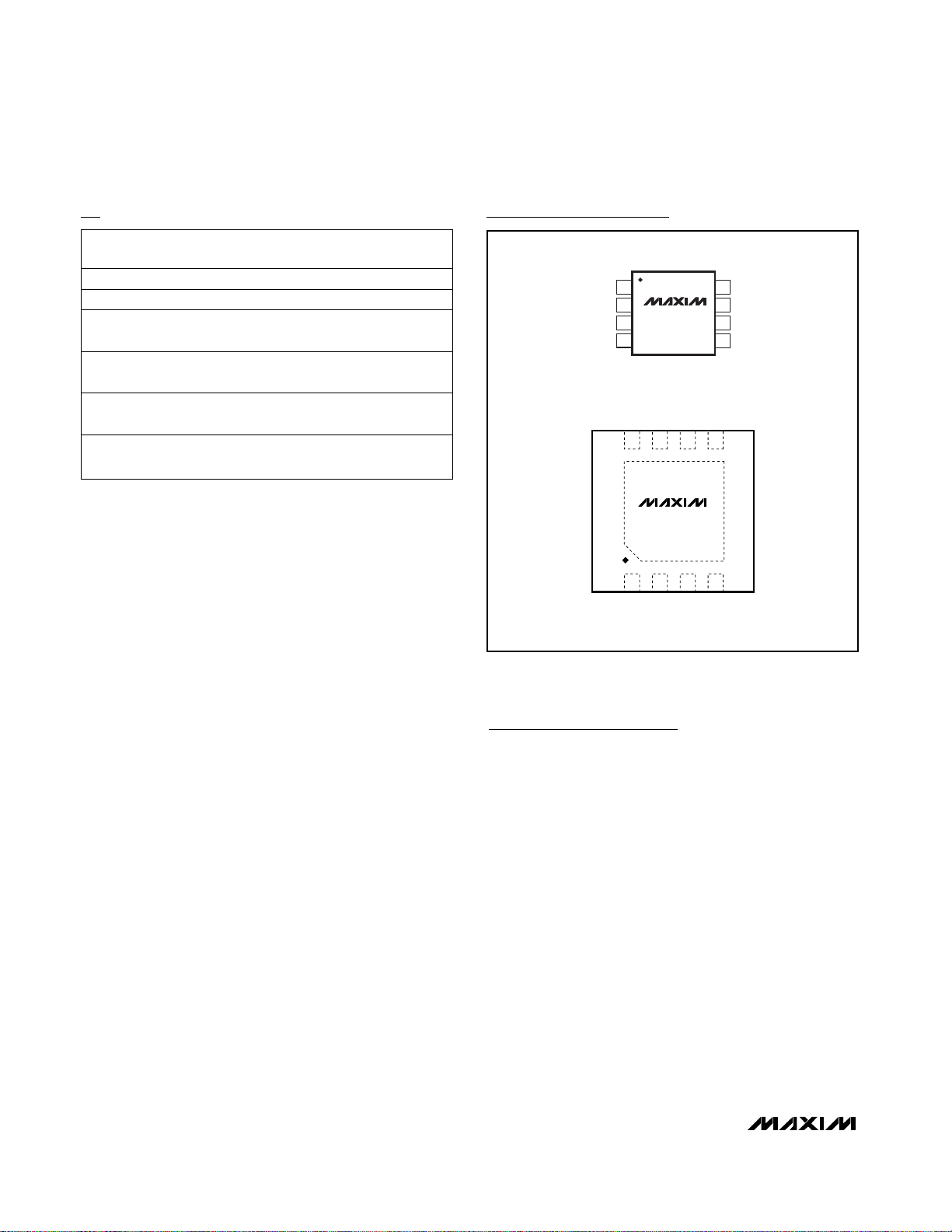
Pin Configuration
134
865
MAX2015
2
7
TDFN
TOP VIEW
OUT SET GND PWDN
V
CC INHI INLOVCC
PACKAGE
-40°C to +85°C
-40°C to +85°C
-40°C to +85°C
-40°C to +85°C
-40°C to +85°C
-40°C to +85°C
8 TDFN-EP*
(3mm x 3mm)
8 TDFN-EP*
(3mm x 3mm)
8 TDFN-EP*
(3mm x 3mm)
8 TDFN-EP*
(3mm x 3mm)
Page 11

MAX2015
0.1GHz to 3GHz, 75dB Logarithmic
Detector/Controller
______________________________________________________________________________________ 11
8LUMAXD.EPS
PACKAGE OUTLINE, 8L uMAX/uSOP
1
1
21-0036
J
REV.DOCUMENT CONTROL NO.APPROVAL
PROPRIETARY INFORMATION
TITLE:
MAX
0.043
0.006
0.014
0.120
0.120
0.198
0.026
0.007
0.037
0.0207 BSC
0.0256 BSC
A2
A1
c
e
b
A
L
FRONT VIEW
SIDE VIEW
E H
0.6±0.1
0.6±0.1
Ø0.50±0.1
1
TOP VIEW
D
8
A2
0.030
BOTTOM VIEW
1
6°
S
b
L
H
E
D
e
c
0°
0.010
0.116
0.116
0.188
0.016
0.005
8
4X S
INCHES
-
A1
A
MIN
0.002
0.950.75
0.5250 BSC
0.25 0.36
2.95 3.05
2.95 3.05
4.78
0.41
0.65 BSC
5.03
0.66
6°0°
0.13 0.18
MAX
MIN
MILLIMETERS
- 1.10
0.05 0.15
α
α
DIM
Package Information
(The package drawing(s) in this data sheet may not reflect the most current specifications. For the latest package outline information,
go to www.maxim-ic.com/packages
.)
Page 12

MAX2015
0.1GHz to 3GHz, 75dB Logarithmic
Detector/Controller
12 ______________________________________________________________________________________
Package Information (continued)
(The package drawing(s) in this data sheet may not reflect the most current specifications. For the latest package outline information,
go to www.maxim-ic.com/packages
.)
6, 8, &10L, DFN THIN.EPS
H
1
2
21-0137
PACKAGE OUTLINE, 6,8,10 & 14L,
TDFN, EXPOSED PAD, 3x3x0.80 mm
Page 13

MAX2015
0.1GHz to 3GHz, 75dB Logarithmic
Detector/Controller
Maxim cannot assume responsibility for use of any circuitry other than circuitry entirely embodied in a Maxim product. No circuit patent licenses are
implied. Maxim reserves the right to change the circuitry and specifications without notice at any time.
Maxim Integrated Products, 120 San Gabriel Drive, Sunnyvale, CA 94086 408-737-7600 ____________________ 13
© 2007 Maxim Integrated Products is a registered trademark of Maxim Integrated Products, Inc.
Package Information (continued)
(The package drawing(s) in this data sheet may not reflect the most current specifications. For the latest package outline information,
go to www.maxim-ic.com/packages
.)
COMMON DIMENSIONS
SYMBOL
MIN. MAX.
A 0.70 0.80
D 2.90 3.10
E 2.90 3.10
A1
0.00 0.05
L 0.20 0.40
PKG. CODE N D2 E2 e JEDEC SPEC b [(N/2)-1] x e
PACKAGE VARIATIONS
0.25 MIN.k
A2 0.20 REF.
2.30±0.101.50±0.106T633-1 0.95 BSC MO229 / WEEA 1.90 REF0.40±0.05
1.95 REF0.30±0.050.65 BSC2.30±0.108T833-1
2.00 REF0.25±0.050.50 BSC2.30±0.1010T1033-1
2.40 REF0.20±0.05- - - - 0.40 BSC1.70±0.10 2.30±0.1014T1433-1
1.50±0.10
1.50±0.10
MO229 / WEEC
MO229 / WEED-3
0.40 BSC - - - - 0.20±0.05 2.40 REFT1433-2 14 2.30±0.101.70±0.10
T633-2 6 1.50±0.10 2.30±0.10
0.95 BSC MO229 / WEEA
0.40±0.05 1.90 REF
T833-2 8 1.50±0.10 2.30±0.10 0.65 BSC MO229 / WEEC 0.30±0.05 1.95 REF
T833-3 8 1.50±0.10 2.30±0.10 0.65 BSC MO229 / WEEC 0.30±0.05 1.95 REF
-DRAWING NOT TO SCALE-
H
2
2
21-0137
PACKAGE OUTLINE, 6,8,10 & 14L,
TDFN, EXPOSED PAD, 3x3x0.80 mm
2.30±0.10
MO229 / WEED-3
2.00 REF0.25±0.05
0.50 BSC
1.50±0.1010T1033-2
Revision History
Pages changed at Rev 2: 1–10, 12, 13
 Loading...