

Page 1
General Description
The MAX2009 adjustable RF predistorter is designed to
improve power amplifier (PA) adjacent-channel power
rejection (ACPR) by introducing gain and phase expansion in a PA chain to compensate for the PA’s gain and
phase compression. With its +23dBm maximum input
power level and wide adjustable range, the MAX2009
can provide up to 12dB of ACPR improvement for
power amplifiers operating in the 1200MHz to 2500MHz
frequency band. Lower frequencies of operation can be
achieved with this IC’s counterpart, the MAX2010.
The MAX2009 is unique in that it provides up to 7dB of
gain expansion and 24° of phase expansion as the
input power is increased. The amount of expansion is
configurable through two independent sets of control:
one set adjusts the gain expansion breakpoint
and slope, while the second set controls the same
parameters for phase. With these settings in place, the
linearization circuit can be run in either a static set-andforget mode, or a more sophisticated closed-loop
implementation can be employed with real-time software-controlled distortion correction. Hybrid correction
modes are also possible using simple lookup tables to
compensate for factors such as PA temperature drift
or PA loading.
The MAX2009 comes in a 28-pin thin QFN exposed
pad (EP) package (5mm x 5mm) and is specified for
the extended (-40°C to +85°C) temperature range.
Applications
WCDMA/UMTS, cdma2000, DCS1800, and
PCS1900 Base Stations
Feed-Forward PA Architectures
Digital Baseband Predistortion Architectures
Military Applications
WLAN Applications
Features
♦ Up to 12dB ACPR Improvement*
♦ Independent Gain and Phase Expansion Controls
♦ Gain Expansion Up to 7dB
♦ Phase Expansion Up to 24°
♦ 1200MHz to 2500MHz Frequency Range
♦ Exceptional Gain and Phase Flatness
♦ Group Delay <1.3ns (Gain and Phase Sections
Combined)
♦ ±0.04ns Group Delay Ripple Over a 100MHz Band
♦ Capable of Handling Input Drives Up to +23dBm
♦ On-Chip Temperature Variation Compensation
♦ Single +5V Supply
♦ Low Power Consumption: 75mW (typ)
♦ Fully Integrated into Small 28-Pin Thin QFN
Package
*Performance dependent on amplifier, bias, and modulation.
MAX2009
1200MHz to 2500MHz Adjustable
RF Predistorter
________________________________________________________________ Maxim Integrated Products 1
28 27 26 25 24 23 22
7
6
5
4
3
2
1
15
16
17
18
19
20
21
8 9 10 11 12 13 14
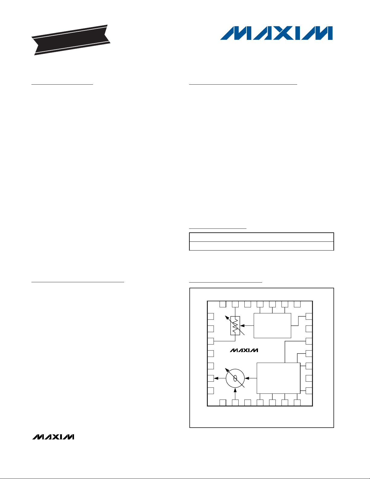
MAX2009
GAIN
CONTROL
PHASE
CONTROL
GND*
GND*
ING
GND*
GND*
OUTP
GND*
V
CCG
GND*
PBRAW
PBEXP
PBIN
GND*
V
CCP
GND*
INP
GND*
PFS1
PFS2
PDCS1
PDCS2
GND*
OUTG
GND*
GCS
GFS
GBP
GND*
*INTERNALLY CONNECTED TO EXPOSED GROUND PADDLE.
Functional Diagram/
Pin Configuration
Ordering Information
19-2929; Rev 0; 8/03
*EP = Exposed paddle.
EVALUATION KIT
AVAILABLE
PART TEMP RANGE PIN-PACKAGE
MAX2009ETI-T -40°C to +85°C
28 Thin QFN-EP*
For pricing, delivery, and ordering information, please contact Maxim Direct at 1-888-629-4642,
or visit Maxim's website at www.maxim-ic.com.
Page 2
MAX2009
1200MHz to 2500MHz Adjustable
RF Predistorter
2 _______________________________________________________________________________________
ABSOLUTE MAXIMUM RATINGS
DC ELECTRICAL CHARACTERISTICS
(MAX2009 EV kit; V
CCG
= V
CCP
= +4.75V to +5.25V; no RF signal applied; INP, ING, OUTP, OUTG are AC-coupled and terminated to
50Ω; V
PF_S1
= open; PBEXP shorted to PBRAW; V
PDCS1
= V
PDCS2
= 0.8V; V
PBIN
= V
GBP
= V
GCS
= GND; V
GFS
= V
CCG
; TA= -40°C to
+85°C. Typical values are at V
CCG
= V
CCP
= +5.0V, TA= +25°C, unless otherwise noted.)
Stresses beyond those listed under “Absolute Maximum Ratings” may cause permanent damage to the device. These are stress ratings only, and functional
operation of the device at these or any other conditions beyond those indicated in the operational sections of the specifications is not implied. Exposure to
absolute maximum rating conditions for extended periods may affect device reliability.
V
CCG
, V
CCP
to GND ..............................................-0.3V to +5.5V
ING, OUTG, GCS, GFS, GBP to GND......-0.3V to (V
CCG
+ 0.3V)
INP, OUTP, PFS_, PDCS_, PBRAW,
PBEXP, PBIN to GND ............................-0.3V to (V
CCP
+ 0.3V)
Input (ING, INP, OUTP, OUTG) Level ............................+23dBm
PBEXP Output Current ........................................................±1mA
Continuous Power Dissipation (T
A
= +70°C)
28-Pin Thin QFN-EP
(derate 21mW/°C above +70°C)...............................1667mW
Operating Temperature Range ...........................-40°C to +85°C
Junction Temperature......................................................+150°C
Storage Temperature Range .............................-65°C to +150°C
Lead Temperature (soldering 10s) ..................................+300°C
PARAMETER CONDITIONS
MIN
TYP
MAX
UNITS
Supply Voltage V
CCG
, V
CCP
V
V
CCP
5.8 7
Supply Current
V
CCG
10
mA
PBIN, PBRAW 0
Analog Input Voltage Range
GBP, GFS, GCS 0
V
V
GFS
= V
GCS
= V
PBRAW
= 0V -2 +2
V
GBP
= 0 to +5V
Analog Input Current
V
PBIN
= 0 to +5V
µA
Logic-Input High Voltage PDCS1, PDCS2 (Note 1) 2.0 V
Logic-Input Low Voltage PDCS1, PDCS2 (Note 1) 0.8 V
Logic Input Current -2 +2 µA
4.75 5.25
-100 +170
-100 +220
12.1
V
CCP
V
CCG
Page 3
MAX2009
1200MHz to 2500MHz Adjustable
RF Predistorter
_______________________________________________________________________________________ 3
AC ELECTRICAL CHARACTERISTICS
(MAX2009 EV kit, V
CCG
= V
CCP
= +4.75V to +5.25V, 50Ω environment, PIN= -20dBm, fIN= 1200MHz to 2500MHz, V
GCS
= +1.0V,
V
GFS
= +5.0V, V
GBP
= +1.2V, V
PBIN
= V
PDCS1
= V
PDCS2
= 0V, V
PF_S1
= +5V, V
PBRAW
= V
PBEXP
, TA= -40°C to +85°C. Typical values
are at f
IN
= 2140MHz, V
CCG
= V
CCP
= +5V, TA= +25°C, unless otherwise noted.) (Notes 1, 2)
PARAMETER CONDITIONS
UNITS
Operating Frequency Range
MHz
VSWR ING, INP, OUTG, OUTP
PHASE CONTROL SECTION
Nominal Gain
dB
Gain Variation Over Temperature
TA = -40°C to +85°C
dB
Gain Flatness Over a 100MHz band
dB
Phase-Expansion Breakpoint
Maximum
V
PBIN
= +5V 23
dBm
Phase-Expansion Breakpoint
Minimum
V
PBIN
= 0V 3.7
dBm
Phase-Expansion Breakpoint
Variation Over Temperature
T
A
= -40°C to +85°C
dB
V
PF_S1
= +5V, V
PDCS1
= V
PDCS2
= 0V,
P
IN
= -20 dBm to +23 dBm
V
PDCS1
= 5V, V
PDCS2
= 0V, V
PF_S1
= +1.5V
V
PDCS1
= 0V, V
PDCS2
= 5V, V
PF_S1
= +1.5V 9.2
Phase Expansion
V
PF_S1
= 0V, V
PDCS1
= V
PDCS2
= +5V,
P
IN
= -20dBm to +23dBm
7.6
Degrees
Phase-Expansion Slope
Maximum
P
IN
= +15dBm 1.2
Degrees
/dB
Phase-Expansion Slope Minimum
V
PF_S1
= 0V, V
PDCS1
= V
PDCS2
= +5V,
P
IN
= +15dBm
0.4
Degrees
/dB
Phase Slope Variation Over
Temperature
P
IN
= +15dBm, TA = -40°C to +85°C
Degrees
/dB
Phase Ripple Over a 100MHz band, deviation from linear phase
Degrees
Noise Figure 7.5 dB
Absolute Group Delay Interconnects de-embedded 0.7 ns
Group Delay Ripple Over a 100MHz band
ns
Parasitic Gain Expansion PIN = -20dBm to +23dBm 0.9 dB
MIN TYP MAX
1200 2500
1.3:1
-7.5
-1.4
±0.1
±1.3
23.7
14.2
-0.1
±0.15
±0.03
Page 4
MAX2009
1200MHz to 2500MHz Adjustable
RF Predistorter
4 _______________________________________________________________________________________
Note 1: Guaranteed by design and characterization.
Note 2: All limits reflect losses and characteristics of external components shown in the Typical Application Circuit, unless otherwise
noted.
AC ELECTRICAL CHARACTERISTICS (continued)
(MAX2009 EV kit, V
CCG
= V
CCP
= +4.75V to +5.25V, 50Ω environment, PIN= -20dBm, fIN= 1200MHz to 2500MHz, V
GCS
= +1.0V,
V
GFS
= +5.0V, V
GBP
= +1.2V, V
PBIN
= V
PDCS1
= V
PDCS2
= 0V, V
PF_S1
= +5V, V
PBRAW
= V
PBEXP
, TA= -40°C to +85°C. Typical values
are at f
IN
= 2140MHz, V
CCG
= V
CCP
= +5V, TA= +25°C, unless otherwise noted.) (Notes 1, 2)
PARAMETER CONDITIONS
GAIN CONTROL SECTION
-16
V
GCS
= 0V, V
GFS
= +5V -23
Nominal Gain
V
GCS
= +5V, V
GFS
= 0V
dB
Gain Variation Over Temperature
TA = -40°C to +85°C-1dB
Gain Flatness Over a 100MHz band
dB
Gain-Expansion Breakpoint
Maximum
V
GBP
= +5V 23
Gain-Expansion Breakpoint
Minimum
V
GBP
= +0.5V -3
Gain-Expansion Breakpoint
Variation Over Temperature
T
A
= -40°C to +85°C
dB
V
GFS
= +5V, PIN = -20dBm to +23dBm 6.6
Gain Expansion
V
GFS
= 0V, PIN = -20dBm to +23dBm 3.6
dB
V
GFS
= +5V, PIN = +15dBm 0.5
Gain-Expansion Slope
V
GFS
= +0V, PIN = +15dBm
Gain Slope Variation Over
Temperature
P
IN
= +15dBm, TA = -40°C to +85°C
Noise Figure 16 dB
Absolute Group Delay Interconnects de-embedded
ns
Group Delay Ripple Over a 100MHz band
ns
Phase Ripple Over a 100MHz band, deviation from linear phase
Parasitic Phase Expansion PIN = -20dBm to +23dBm 5
MIN TYP MAX UNITS
-8.5
±0.3
-0.3
0.26
-0.04 dB/dB
0.61
±0.01
±0.07 Degrees
dBm
dBm
dB/dB
Degrees
Page 5
MAX2009
1200MHz to 2500MHz Adjustable
RF Predistorter
_______________________________________________________________________________________ 5
5.3
5.6
5.5
5.4
5.7
5.8
5.9
6.0
6.1
6.2
6.3
4.75 4.954.85 5.05 5.15 5.25
SUPPLY CURRENT
vs. SUPPLY VOLTAGE
MAX2009TOC01
SUPPLY VOLTAGE (V)
SUPPLY CURRENT (mA)
TA = +85°C
TA = +25°C
TA = -40°C
SMALL-SIGNAL INPUT RETURN LOSS
vs. FREQUENCY
MAX2009TOC02
40
35
25
30
10
5
15
20
0
INPUT RETURN LOSS (dB)
1.1 1.5 1.71.3
1.9
2.1 2.3 2.5
FREQUENCY (GHz)
A = V
PDCS1
= V
PDCS2
= V
PF_S1
= 0V
B = V
PDCS1
= V
PDCS2
= 0V, V
PF_S1
= 5V
C = V
PDCS1
= V
PDCS2
= 5V, V
PF_S1
= 0V
D = V
PDCS1
= V
PDCS2
= V
PF_S1
= 5V
B
D
C
A
SMALL-SIGNAL OUTPUT RETURN LOSS
vs. FREQUENCY
MAX2009TOC03
40
35
25
30
10
5
15
20
0
OUTPUT RETURN LOSS (dB)
1.1 1.5 1.71.3
1.9
2.1 2.3 2.5
FREQUENCY (GHz)
A = V
PDCS1
= V
PDCS2
= V
PF_S1
= 0V
B = V
PDCS1
= V
PDCS2
= 0V, V
PF_S1
= 5V
C = V
PDCS1
= V
PDCS2
= 5V, V
PF_S1
= 0V
D = V
PDCS1
= V
PDCS2
= V
PF_S1
= 5V
B
C
A
D
LARGE-SIGNAL INPUT RETURN LOSS
vs. FREQUENCY
MAX2009TOC04
40
35
25
30
10
5
15
20
0
INPUT RETURN LOSS (dB)
1.1 1.5 1.71.3
1.9
2.1 2.3 2.5
FREQUENCY (GHz)
A = V
PDCS1
= V
PDCS2
= V
PF_S1
= 0V
B = V
PDCS1
= V
PDCS2
= 0V, V
PF_S1
= 5V
C = V
PDCS1
= V
PDCS2
= 5V, V
PF_S1
= 0V
D = V
PDCS1
= V
PDCS2
= V
PF_S1
= 5V
C
D
B
A
PIN = +15dBm
LARGE-SIGNAL OUTPUT RETURN LOSS
vs. FREQUENCY
MAX2009TOC05
40
35
25
30
10
5
15
20
0
OUTPUT RETURN LOSS (dB)
1.1 1.5 1.71.3
1.9
2.1 2.3 2.5
FREQUENCY (GHz)
A = V
PDCS1
= V
PDCS2
= V
PF_S1
= 0V
B = V
PDCS1
= V
PDCS2
= 0V, V
PF_S1
= 5V
C = V
PDCS1
= V
PDCS2
= 5V, V
PF_S1
= 0V
D = V
PDCS1
= V
PDCS2
= V
PF_S1
= 5V
C
D
B
A
PIN = +15dBm
-10.0
-8.5
-9.0
-9.5
-7.5
-8.0
-5.5
-6.0
-6.5
-7.0
-5.0
1.1 1.3 1.5 1.7 1.9 2.1 2.3 2.5
SMALL-SIGNAL GAIN
vs. FREQUENCY
MAX2009TOC06
FREQUENCY (GHz)
GAIN (dB)
TA = +85°C
TA = +25°C
TA = -40°C
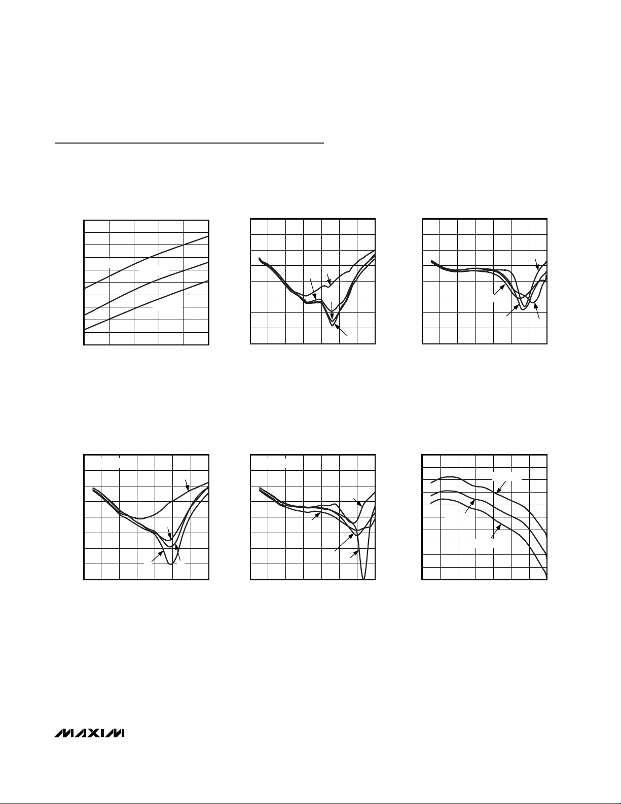
Typical Operating Characteristics
Phase Control Section
(MAX2009 EV kit, V
CCP
= +5.0V, PIN= -20dBm, V
PBIN
= 0V, V
PF_S1
= +5.0V, V
PDCS1
= V
PDCS2
= 0V, fIN= 2140MHz, TA= +25°C,
unless otherwise noted.)
Page 6
MAX2009
1200MHz to 2500MHz Adjustable
RF Predistorter
6 _______________________________________________________________________________________
-10.0
-8.5
-9.0
-9.5
-7.5
-8.0
-5.5
-6.0
-6.5
-7.0
-5.0
1.1 1.3 1.5 1.7 1.9 2.1 2.3 2.5
SMALL-SIGNAL GAIN
vs. FREQUENCY
MAX2009TOC07
FREQUENCY (GHz)
GAIN (dB)
V
CCP
= 4.75V, 5.0V, 5.25V
-8.0
-7.5
-6.5
-7.0
-6.0
-5.5
SMALL-SIGNAL GAIN
vs. COARSE SLOPE
MAX2009TOC08
COARSE SLOPE (V)
GAIN (dB)
PDCS1 = 0,
PDCS2 = 5
PDCS1 = 5,
PDCS2 = 5
PDCS1 = 5,
PDCS2 = 0
PDCS1 = 0,
PDCS2 = 0
V
PF_S1
= 1.5V
V
PF_S1
= 0V
V
PF_S1
= 5V
-8.0
-7.5
-6.5
-7.0
-6.0
-5.5
SMALL-SIGNAL GAIN
vs. COARSE SLOPE
MAX2009TOC09
COARSE SLOPE (V)
GAIN (dB)
TA = -40°C
TA = +25°C
TA = +85°C
PDCS1 = 0,
PDCS2 = 5
PDCS1 = 5,
PDCS2 = 5
PDCS1 = 5,
PDCS2 = 0
PDCS1 = 0,
PDCS2 = 0
GROUP DELAY
vs. FREQUENCY
MAX2009TOC10
0.50
0.60
0.55
0.75
0.80
0.70
0.65
0.85
DELAY (ns)
1.1 1.5 1.71.3
1.9
2.1 2.3 2.5
FREQUENCY (GHz)
A = V
PDCS1
= V
PDCS2
= V
PF_S1
= 0V
B = V
PDCS1
= V
PDCS2
= 0V, V
PF_S1
= 5V
C = V
PDCS1
= V
PDCS2
= 5V, V
PF_S1
= 0V
D = V
PDCS1
= V
PDCS2
= V
PF_S1
= 5V
D
C
A
B
INTERCONNECTS DE-EMBEDDED
NOISE FIGURE vs. FREQUENCY
MAX2009TOC11
5.0
6.5
5.5
6.0
8.0
8.5
9.0
7.5
7.0
9.5
NOISE FIGURE (dB)
1.5 1.7 1.9
2.1
2.3 2.5
FREQUENCY (GHz)
A = V
PDCS1
= V
PDCS2
= V
PF_S1
= 0V
B = V
PDCS1
= V
PDCS2
= 0V, V
PF_S1
= 5V
C = V
PDCS1
= V
PDCS2
= 5V, V
PF_S1
= 0V
D = V
PDCS1
= V
PDCS2
= V
PF_S1
= 5V
D
C
A
B
5.70
5.80
5.75
5.90
5.85
5.95
6.00
SUPPLY CURRENT vs. INPUT POWER
MAX2009TOC12
INPUT POWER (dBm)
SUPPLY CURRENT (mA)
08124162024
A = V
PBIN
= 0V
B = V
PBIN
= 0.5V
C = V
PBIN
= 1.0V
D
E
C
A
B
D = V
PBIN
= 1.5V
E = V
PBIN
= 3.0V
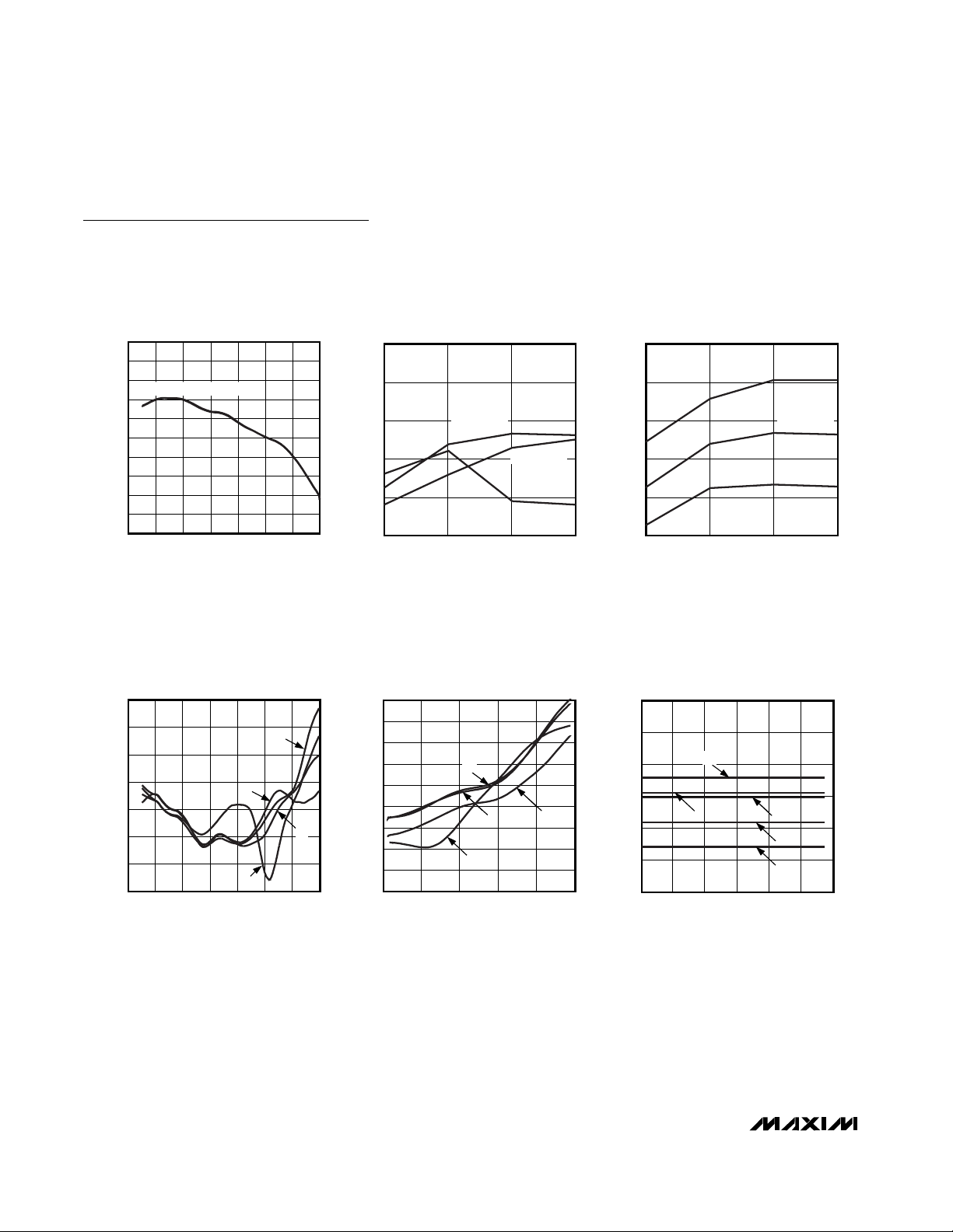
Typical Operating Characteristics (continued)
Phase Control Section (continued)
(MAX2009 EV kit, V
CCP
= +5.0V, PIN= -20dBm, V
PBIN
= 0V, V
PF_S1
= +5.0V, V
PDCS1
= V
PDCS2
= 0V, fIN= 2140MHz, TA= +25°C,
unless otherwise noted.)
Page 7
MAX2009
1200MHz to 2500MHz Adjustable
RF Predistorter
_______________________________________________________________________________________ 7
-7.8
-7.4
-7.6
-6.6
-7.0
-6.2
-6.8
-7.2
-6.4
-6.0
GAIN EXPANSION vs. INPUT POWER
MAX2009TOC13
INPUT POWER (dBm)
GAIN (dB)
-7 3 8-2 13 18 23
A = V
PBIN
= 0V
B = V
PBIN
= 0.5V
C = V
PBIN
= 1.0V
D
E
F
A
B
D = V
PBIN
= 1.5V
E = V
PBIN
= 2.0V
F = V
PBIN
= 2.5V
C
150
190
PHASE EXPANSION vs. INPUT POWER
MAX2009TOC14
INPUT POWER (dBm)
PHASE (DEGREES)
180
160
170
-7 3 8-2 13 18 23
A = V
PBIN
= 0V
B = V
PBIN
= 0.5V
C = V
PBIN
= 1.0V
D
E
F
A
B
D = V
PBIN
= 1.5V
E = V
PBIN
= 2.0V
F = V
PBIN
= 2.5V
C
-7.8
-7.4
-7.6
-6.6
-7.0
-6.2
-6.8
-7.2
-6.4
-6.0
GAIN EXPANSION vs. INPUT POWER
MAX2009TOC15
INPUT POWER (dBm)
GAIN (dB)
-7 3 8-2 13 18 23
A = V
PDCS1
= V
PDCS2
= 0V
B = V
PDCS1
= 5V, V
PDCS2
= 0V
D
A
B
C
C = V
PDCS1
= 0V, V
PDCS2
= 5V
D = V
PDCS1
= V
PDCS2
= 5V
-7.8
-7.4
-7.6
-6.6
-7.0
-6.2
-6.8
-7.2
-6.4
-6.0
GAIN EXPANSION vs. INPUT POWER
MAX2009TOC16
INPUT POWER (dBm)
GAIN (dB)
-7 3 8-2 13 18 23
A = V
PF_S1
= 0V
B = V
PF_S1
= 0.5V
C = V
PF_S1
= 1.0V
D = V
PF_S1
= 1.5V
E
A
B
E = V
PF_S1
= 2.0V
F = V
PF_S1
= 5.0V
V
PDCS1
= 5.0V
C
D
F
150
190
PHASE EXPANSION vs. INPUT POWER
MAX2009TOC17
INPUT POWER (dBm)
PHASE (DEGREES)
180
160
170
-7 3 8-2 13 18 23
A = V
PF_S1
= 0V
B = V
PF_S1
= 0.5V
C = V
PF_S1
= 1.0V
D
E
F
A
B
D = V
PF_S1
= 1.5V
E = V
PF_S1
= 2.0V
F = V
PF_S1
= 5.0V
V
PDCS1
= 5.0V
C
150
190
PHASE EXPANSION vs. INPUT POWER
MAX2009TOC18
INPUT POWER (dBm)
PHASE (DEGREES)
180
160
170
-7 3 8-2 13 18 23
A = V
PDCS1
= V
PDCS2
= 0V
B = V
PDCS1
= 5V, V
PDCS2
= 0V
A
D
C
C = V
PDCS1
= 0V, V
PDCS2
= 5V
D = V
PDCS1
= V
PDCS2
= 5V
B
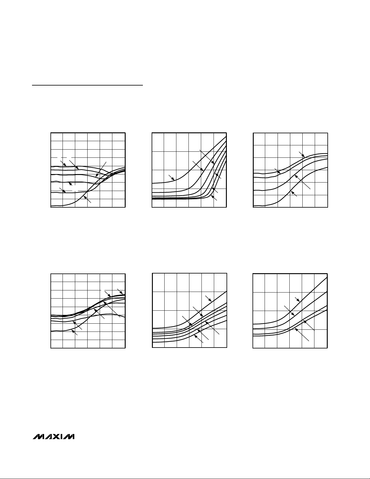
Typical Operating Characteristics (continued)
Phase Control Section (continued)
(MAX2009 EV kit, V
CCP
= +5.0V, PIN= -20dBm, V
PBIN
= 0V, V
PF_S1
= +5.0V, V
PDCS1
= V
PDCS2
= 0V, fIN= 2140MHz, TA= +25°C,
unless otherwise noted.)
Page 8
MAX2009
1200MHz to 2500MHz Adjustable
RF Predistorter
8 _______________________________________________________________________________________
-7.8
-6.8
-7.3
-5.8
-6.3
-5.3
GAIN EXPANSION vs. INPUT POWER
MAX2009TOC19
INPUT POWER (dBm)
GAIN (dB)
-7 3 8-2 13 18 23
V
PDCS1
= 5.0, V
PF_S1
= 1.5V
T
A
= -40°C
T
A
= +25°C
T
A
= +85°C
150
160
165
155
175
170
180
PHASE EXPANSION vs. INPUT POWER
INPUT POWER (dBm)
PHASE (DEGREES)
-7 3 8-2 13 18 23
V
PDCS1
= 5.0, V
PF_S1
= 1.5V
T
A
= -40°C
T
A
= +25°C
T
A
= +85°C
MAX2009TOC20
8.0
8.4
8.2
8.8
8.6
9.2
9.0
9.4
4.75 4.954.85 5.05 5.15 5.25
SUPPLY CURRENT vs. SUPPLY VOLTAGE
MAX2009TOC21
SUPPLY VOLTAGE (V)
SUPPLY CURRENT (mA)
TA = +85°C
T
A
= +25°C
T
A
= -40°C
40
30
35
20
25
10
5
15
0
1.1 1.7 1.91.51.3 2.1 2.3 2.5
SMALL-SIGNAL INPUT RETURN LOSS
vs. FREQUENCY
MAX2009TOC22
FREQUENCY (GHz)
INPUT RETURN LOSS (dB)
A = V
GCS
= 0V, V
GFS
= 0V
B = V
GCS
= 0V, V
GFS
= 5V
C = V
GCS
= 5V, V
GFS
= 0V
D = V
GCS
= 5V, V
GFS
= 5V
A
B
D
C
40
30
35
20
25
10
5
15
0
1.1 1.7 1.91.51.3 2.1 2.3 2.5
SMALL-SIGNAL OUTPUT RETURN LOSS
vs. FREQUENCY
MAX2009TOC23
FREQUENCY (GHz)
OUTPUT RETURN LOSS (dB)
A = V
GCS
= 0V, V
GFS
= 0V
B = V
GCS
= 0V, V
GFS
= 5V
C = V
GCS
= 5V, V
GFS
= 0V
D = V
GCS
= 5V, V
GFS
= 5V
B
A
D
C
Typical Operating Characteristics
Gain Control Section
(MAX2009 EV kit, V
CCG
= +5.0V, PIN= -20dBm, V
GBP
= +1.2V, V
GFS
= +5.0V, V
GCS
= +1.0V, fIN= 2140MHz, TA= +25°C, unless
otherwise noted.)
Typical Operating Characteristics (continued)
Phase Control Section (continued)
(MAX2009 EV kit, V
CCP
= +5.0V, PIN= -20dBm, V
PBIN
= 0V, V
PF_S1
= +5.0V, V
PDCS1
= V
PDCS2
= 0V, fIN= 2140MHz, TA= +25°C,
unless otherwise noted.)
Page 9

MAX2009
1200MHz to 2500MHz Adjustable
RF Predistorter
_______________________________________________________________________________________ 9
40
30
35
20
25
10
5
15
0
1.1 1.7 1.91.51.3 2.1 2.3 2.5
LARGE-SIGNAL OUTPUT RETURN LOSS
vs. FREQUENCY
MAX2009TOC25
FREQUENCY (GHz)
OUTPUT RETURN LOSS (dB)
A = V
GCS
= 0V, V
GFS
= 0V
B = V
GCS
= 0V, V
GFS
= 5V
C = V
GCS
= 5V, V
GFS
= 0V
D = V
GCS
= 5V, V
GFS
= 5V
B
A
D
C
PIN = +15dBm
-20
-18
-19
-16
-17
-14
-13
-15
-12
1.1 1.7 1.91.51.3 2.1 2.3 2.5
SMALL-SIGNAL GAIN vs. FREQUENCY
MAX2009TOC26
FREQUENCY (GHz)
GAIN (dB)
TA = -40°C
T
A
= +85°C
T
A
= +25°C
-20
-18
-19
-16
-17
-14
-13
-15
-12
1.1 1.7 1.91.51.3 2.1 2.3 2.5
SMALL-SIGNAL GAIN vs. FREQUENCY
MAX2009TOC27
FREQUENCY (GHz)
GAIN (dB)
V
CCG
= 4.75V, 5.0V, 5.25V
-25
-21
-23
-17
-19
-13
-9
-11
-15
-7
034215
SMALL-SIGNAL GAIN vs. V
GCS
MAX2009TOC28
V
GCS
(V)
GAIN (dB)
V
GFS
= 0V, 1.5V, 5.0V
-25
-21
-23
-17
-19
-13
-9
-11
-15
-7
034215
SMALL-SIGNAL GAIN vs. V
GCS
MAX2009TOC29
V
GCS
(V)
GAIN (dB)
TA = +85°C
TA = -40°C
T
A
= +25°C
40
30
35
20
25
10
5
15
0
1.1 1.7 1.91.51.3 2.1 2.3 2.5
LARGE-SIGNAL INPUT RETURN LOSS
vs. FREQUENCY
MAX2009TOC24
FREQUENCY (GHz)
INPUT RETURN LOSS (dB)
A = V
GCS
= 0V, V
GFS
= 0V
B = V
GCS
= 0V, V
GFS
= 5V
C = V
GCS
= 5V, V
GFS
= 0V
D = V
GCS
= 5V, V
GFS
= 5V
B
A
D
C
PIN = +15dBm
Typical Operating Characteristics (continued)
Gain Control Section (continued)
(MAX2009 EV kit, V
CCG
= +5.0V, PIN= -20dBm, V
GBP
= +1.2V, V
GFS
= +5.0V, V
GCS
= +1.0V, fIN= 2140MHz, TA= +25°C, unless
otherwise noted.)
Page 10

MAX2009
1200MHz to 2500MHz Adjustable
RF Predistorter
10 ______________________________________________________________________________________
NOISE FIGURE vs. FREQUENCY
MAX2009TOC31
6
8
12
10
18
22
20
24
16
14
26
NOISE FIGURE (dB)
1.5 1.7
1.9
2.1 2.3 2.5
FREQUENCY (GHz)
A = V
GCS
= 0V, V
GFS
= 0V
B = V
GCS
= 0V, V
GFS
= 5V
C = V
GCS
= 1.5V, V
GFS
= 5V
B
D
E
C
A
D = V
GCS
= 5V, V
GFS
= 0V
E = V
GCS
= 5V, V
GFS
= 5V
SUPPLY CURRENT vs. INPUT POWER
MAX2009TOC32
5
10
20
25
15
30
SUPPLY CURRENT (mA)
04812 2016 24
INPUT POWER (dBm)
A = V
GBP
= 0V
B = V
GBP
= 0.5V
C = V
GBP
= 1.0V
B
E
D
C
A
D = V
GBP
= 1.5V
E = V
GBP
= 3.0V
GAIN EXPANSION vs. INPUT POWER
MAX2009TOC33
-23
-21
-13
-9
-17
-15
-11
-19
-7
GAIN (dB)
-7 -2
3
81813 23
INPUT POWER (dBm)
A = V
GBP
= 0V
B = V
GBP
= 0.5V
C = V
GBP
= 1.0V
D = V
GBP
= 1.5V
B
C
D
A
E = V
GBP
= 2.0V
F = V
GBP
= 2.5V
G = V
GBP
= 3.5V
H = V
GBP
= 5.0V
G
F
E
H
PHASE EXPANSION vs. INPUT POWER
MAX2009TOC34
130
140
160
180
150
170
190
PHASE (DEGREES)
-7 -2
3
81813 23
INPUT POWER (dBm)
A = V
GBP
= 0V
B = V
GBP
= 0.5V
C = V
GBP
= 1.0V
D = V
GBP
= 1.5V
B
C
D
A
E = V
GBP
= 2.0V
F = V
GBP
= 2.5V
G = V
GBP
= 3.5V
H = V
GBP
= 5.0V
G
FE
H
Typical Operating Characteristics (continued)
Gain Control Section (continued)
(MAX2009 EV kit, V
CCG
= +5.0V, PIN= -20dBm, V
GBP
= +1.2V, V
GFS
= +5.0V, V
GCS
= +1.0V, fIN= 2140MHz, TA= +25°C, unless
otherwise noted.)
0.45
0.55
0.50
0.65
0.60
0.70
0.75
1.1 1.7 1.91.51.3 2.1 2.3 2.5
GROUP DELAY vs. FREQUENCY
MAX2009TOC30
FREQUENCY (GHz)
DELAY (ns)
A = V
GCS
= 0V, V
GFS
= 0V
B = V
GCS
= 0V, V
GFS
= 5V
INTERCONNECTS DE-EMBEDDED
C = V
GCS
= 5V, V
GFS
= 0V
D = V
GCS
= 5V, V
GFS
= 5V
B
A
C
D
Page 11
MAX2009
1200MHz to 2500MHz Adjustable
RF Predistorter
______________________________________________________________________________________ 11
PHASE EXPANSION vs. INPUT POWER
MAX2009TOC37
130
160
180
140
150
170
190
PHASE (DEGREES)
-7 -2
3
81813 23
INPUT POWER (dBm)
A = V
GCS
= 0V
B = V
GCS
= 0.5V
C = V
GCS
= 1.0V
E
F
C
D
A, B
D = V
GCS
= 1.5V
E = V
GCS
= 2.0V
F = V
GCS
= 2.5V
PHASE EXPANSION vs. INPUT POWER
MAX2009TOC38
130
160
180
140
150
170
190
PHASE (DEGREES)
-7 -2
3
81813 23
INPUT POWER (dBm)
A = V
GFS
= 0V
B = V
GFS
= 0.5V
C = V
GFS
= 1.0V
E
F
C
D
A, B
D = V
GFS
= 1.5V
E = V
GFS
= 2.0V
F = V
GFS
= 5.0V
GAIN EXPANSION vs. INPUT POWER
MAX2009TOC39
-17
-16
-15
-14
-11
-9
-13
-12
-10
-8
GAIN (dB)
-7 -2
3
81813 23
INPUT POWER (dBm)
TA = -40°C
T
A
= +25°C
T
A
= +85°C
PHASE EXPANSION vs. INPUT POWER
MAX2009TOC40
140
148
156
144
142
146
152
150
158
154
160
PHASE (DEGREES)
-7 -2
3
81813 23
INPUT POWER (dBm)
TA = -40°C
T
A
= +25°C
T
A
= +85°C
GAIN EXPANSION vs. INPUT POWER
MAX2009TOC35
-23
-21
-13
-9
-17
-15
-11
-19
-7
GAIN (dB)
-7 -2
3
81813 23
INPUT POWER (dBm)
A = V
GFS
= 0V
B = V
GFS
= 0.5V
C = V
GFS
= 1.0V
E
F
C
D
A, B
D = V
GFS
= 1.5V
E = V
GFS
= 2.0V
F = V
GFS
= 5.0V
GAIN EXPANSION vs. INPUT POWER
MAX2009TOC36
-23
-21
-13
-9
-17
-15
-11
-19
-7
GAIN (dB)
-7 -2
3
81813 23
INPUT POWER (dBm)
A = V
GCS
= 0V
B = V
GCS
= 0.5V
C = V
GCS
= 1.0V
F
E
C
D
A, B
D = V
GCS
= 1.5V
E = V
GCS
= 2.0V
F = V
GCS
= 2.5V
Typical Operating Characteristics (continued)
Gain Control Section (continued)
(MAX2009 EV kit, V
CCG
= +5.0V, PIN= -20dBm, V
GBP
= +1.2V, V
GFS
= +5.0V, V
GCS
= +1.0V, fIN= 2140MHz, TA= +25°C, unless
otherwise noted.)
Page 12

MAX2009
1200MHz to 2500MHz Adjustable
RF Predistorter
12 ______________________________________________________________________________________
Detailed Description
The MAX2009 adjustable predistorter can provide up to
12dB of ACPR improvement for high-power amplifiers by
introducing gain and phase expansion to compensate
for the PA’s gain and phase compression. The MAX2009
enables real-time software-controlled distortion correction, as well as set-and-forget tuning through the adjustment of the expansion starting point (breakpoint) and the
rate of expansion (slope). The gain and phase break-
points can be set over a 20dB input power range. The
phase expansion slope is variable from 0.3°/dB to
2.0°/dB and can be adjusted for a maximum of 24° of
phase expansion. The gain expansion slope is variable
from 0.1dB/dB to 0.6dB/dB and can be adjusted for a
maximum of 7dB gain expansion.
The following sections describe the tuning methodology
best implemented with a class A amplifier. Other classes
of operation may require significantly different settings.
Pin Description
PIN NAME FUNCTION
1, 2, 4, 5, 7,
8, 10, 16, 20,
22, 26, 28
GND Ground. Internally connected to the exposed paddle.
3 ING
RF Gain Input. Connect ING to a coupling capacitor if it is not connected to OUTP. ING is
interchangeable with OUTG.
6 OUTP
RF Phase Output. Connect OUTP to a coupling capacitor if it is not connected to INP. OUTP is
interchangeable with INP.
9 INP RF Phase Input. Connect INP to a coupling capacitor. This pin is interchangeable with OUTP.
11 PFS1 Fine Phase-Slope Control Input 1. See the Typical Application Circuit.
12 PFS2 Fine Phase-Slope Control Input 2. See the Typical Application Circuit.
13 PDCS1 Digital Coarse Phase-Slope Control Range Input 1. Set to logical zero for the steepest slope.
14 PDCS2 Digital Coarse Phase-Slope Control Range Input 2. Set to logical zero for the steepest slope.
15 V
CCP
Phase-Control Supply Voltage. Bypass with a 0.01µF capacitor to ground as close to the device as
possible. Phase section can operate without V
CCG
.
17 PBIN Phase Breakpoint Control Input
18 PBEXP Phase Expansion Output. Connect PBEXP to PBRAW to use PBIN as the breakpoint control voltage.
19 PBRAW Uncompensated Phase Breakpoint Input
21 V
CCG
Gain-Control Supply Voltage. Bypass with a 0.01µF capacitor to ground as close to the device as
possible. Gain section can operate without V
CCP
.
23 GBP Gain Breakpoint Control Input
24 GFS Fine Gain-Slope Control Input
25 GCS Coarse Gain-Slope Control Input
27 OUTG RF Gain Output. Connect OUTG to a coupling capacitor. OUTG is interchangeable with ING.
EP GND Exposed Ground Paddle. Solder EP to the ground plane.
Page 13

MAX2009
1200MHz to 2500MHz Adjustable
RF Predistorter
______________________________________________________________________________________ 13
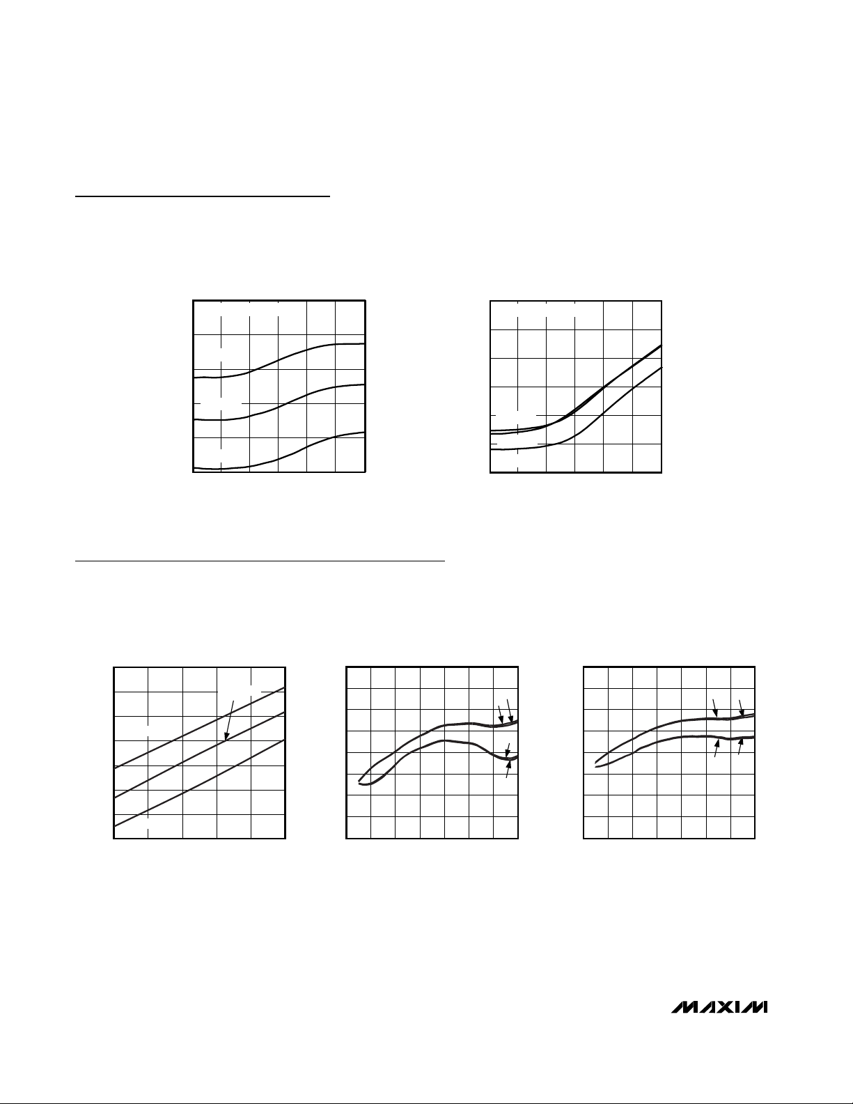
Phase Expansion Circuitry
Figure 1 shows a typical PA’s phase behavior with
respect to input power. For input powers less than the
breakpoint level, the phase remains relatively constant.
As the input power becomes greater than the breakpoint level, the phase begins to compress and deteriorate the power amplifier’s linearity. To compensate for
this AM-PM distortion, the MAX2009 provides phase
expansion, which occurs at the same breakpoint level
but with the opposite slope. The overall result is a flat
phase response.
Phase Expansion Breakpoint
The phase expansion breakpoint is typically controlled
by a digital-to-analog converter (DAC) connected
through the PBIN pin. The PBIN input voltage range of
0V to VCCcorresponds to a breakpoint input power
range of 3.7dBm to 23dBm. To achieve optimal performance, the phase expansion breakpoint of the
MAX2009 must be set to equal the phase compression
breakpoint of the PA.
Phase Expansion Slope
The phase expansion slope of the MAX2009 must also
be adjusted to equal the opposite slope of the PA’s
phase compression curve. The phase expansion slope
of the MAX2009 is controlled by the PFS1, PFS2, PDCS1,
and PDCS2 pins. With pins PFS1 and PFS2, AC-coupled
and connected to a variable capacitor or varactor diode,
the PFS1 and PFS2 pins perform the task of fine tuning
the phase expansion slope. Since off-chip varactor
diodes are recommended for this function, they must
be closely matched and identically biased. A minimum
effective capacitance of 2pF to 6pF is required to
achieve the full phase slope range as specified in the
Electrical Characteristics tables.
As shown in Figure 2, the varactors connected to PFS1
and PFS2 are in series with three internal capacitors on
each pin. By connecting and disconnecting these internal capacitors, a larger change in phase expansion
slope can be achieved through the logic levels presented at the PDCS1 and PDCS2 pins. The phase expansion slope is at its maximum when both V
PDCS1
and
V
PDCS2
equal 0V. The phase tuning has a minimal
effect on the small-signal gain.
Gain Expansion Circuitry
In addition to phase compression, the PA also suffers
from gain compression (AM-AM) distortion, as shown in
Figure 3. The PA gain curve remains flat for input powers below the breakpoint level, and begins to compress
at a given rate (slope) for input powers greater than the
breakpoint level. To compensate for such gain compression, the MAX2009 generates a gain expansion,
which occurs at the same breakpoint level with the
opposite slope. The overall result is a flat gain response
at the PA output.
COMBINED PHASE (DEGREES)
IMPROVED
PHASE DISTORTION
MAX2009 PHASE (DEGREES)
MAX2009
PHASE EXPANSION
PA PHASE (DEGREES)
BREAKPOINT
PA PHASE
COMPRESSION
SLOPE
P
IN
(dBm) P
IN
(dBm) P
IN
(dBm)
Figure 1. PA Phase Compression Canceled by MAX2009 Phase Expansion
Page 14

MAX2009
1200MHz to 2500MHz Adjustable
RF Predistorter
14 ______________________________________________________________________________________
MAX2009
PF_S1
PFS1
PFS2
PDCS1
PDCS2
PHASE-CONTROL
CIRCUITRY
SWITCH
CONTROL
2
Figure 2. Simplified Phase Slope Internal Circuitry
BREAKPOINT
SLOPE
P
IN
(dBm) P
IN
(dBm) P
IN
(dBm)
PA GAIN (dB)
MAX2009 GAIN (dB)
COMBINED GAIN (dB)
PA GAIN
COMPRESSION
MAX2009
GAIN EXPANSION
IMPROVED
GAIN DISTORTION
Figure 3. PA Gain Compression Canceled by MAX2009 Gain Expansion
Page 15

MAX2009
1200MHz to 2500MHz Adjustable
RF Predistorter
______________________________________________________________________________________ 15
Gain Expansion Breakpoint
The gain expansion breakpoint is usually controlled by a
DAC connected through the GBP pin. The GBP input
voltage range of 0.5V to 5V corresponds to a breakpoint
input power range of 3dBm to 23dBm. To achieve the
optimal performance, the gain expansion breakpoint of
the MAX2009 must be set to equal the gain compression point of the PA. The GBP control has a minimal
effect on the small-signal gain when operated from 0.5V
to 5V.
Gain Expansion Slope
In addition to properly setting the breakpoint, the gain
expansion slope of the MAX2009 must also be adjusted
to compensate for the PA’s gain compression. The
slope should be set using the following equation:
where:
MAX2009_SLOPE = MAX2009 gain section’s slope in
dB/dB.
PA_SLOPE = PA’s gain slope in dB/dB, a negative
number for compressive behavior.
To modify the gain expansion slope, two adjustments
must be made to the biases applied on pins GCS and
GFS. Both GCS and GFS have an input voltage range of
0V to VCC, corresponding to a slope of approximately
0.1dB/dB to 0.6dB/dB. The slope is set to maximum
when V
GCS
= 0V and V
GFS
= +5V, and the slope is at its
minimum when V
GCS
= +5V and V
GFS
= 0V.
Unlike the GBP pin, modifying the gain expansion slope
bias on the GCS pin causes a change in the part’s insertion loss and noise figure. For example, a smaller slope
caused by GCS results in a better insertion loss and
lower noise figure. The GFS does not affect the insertion
loss. It can provide up to -30% or +30% total slope variation around the nominal slope set by GCS.
Large amounts of GCS bias adjustment can also lead to
an undesired (or residual) phase expansion/compression behavior. There exists an optimal bias voltage that
minimizes this parasitic behavior (typically GCS = 1.0V).
Control voltages higher than the optimal result in parasitic phase expansion, lower control voltages result in
phase compression. GFS does not contribute to the
phase behavior and is preferred for slope control.
Applications Information
The following section describes the tuning methodology
best implemented with a class A amplifier. Other classes
of operation may require significantly different settings.
Gain and Phase Expansion Optimization
The best approach to improve the ACPR of a PA is to
first optimize the AM-PM response of the phase section. For most high-frequency LDMOS amplifiers,
improving the AM-PM response provides the bulk of the
ACPR improvement. Figure 4 shows a typical configuration of the phase tuning circuit. A power sweep on a
network analyzer allows quick real-time tuning of the
AM-PM response. First, tune PBIN to achieve the phase
expansion starting point (breakpoint) at the same point
where the PA’s phase compression begins. Next, use
control pins PF_S1, PDCS1, and PDCS2 to obtain the
optimal AM-PM response. The typical values for these
pins are shown in Figure 4.
To further improve the ACPR, connect the phase output to the gain input through a preamplifier. The preamplifier is used to compensate for the high insertion
loss of the gain section. Figure 5 shows a typical application circuit of the MAX2009 with the phase section
cascaded to the gain section for further ACPR optimization. Similar to tuning the phase section, first tune
the gain expansion breakpoint through the GBP pin
and adjust for the desired gain expansion with pins
GCS and GFS. To minimize the effect of GCS on the
parasitic phase response, minimize the control voltage
to around 1V. Some retuning of the AM-PM response
may be necessary.
Layout Considerations
A properly designed PC board is an essential part of
any high-frequency circuit. To minimize external components, the PC board can be designed to incorporate
small values of inductance and capacitance to optimize
the input and output VSWR (refer to the MAX2009). The
phase section’s PFS1 and PFS2 pins are sensitive to
external parasitics. Minimize trace lengths and keep
varactor diodes close to the pins. Remove the ground
plane underneath the traces can further help reduce
the parasitic capacitance. For best performance, route
the ground pin traces directly to the grounded EP
underneath the package. Solder the EP on the bottom
of the device package evenly to the board ground
plane to provide a heat transfer path along with signal
grounding.
MAX SLOPE
PA SLOPE
PA SLOPE
20091_
_
_
=
−
+
Page 16
MAX2009
1200MHz to 2500MHz Adjustable
RF Predistorter
16 ______________________________________________________________________________________
Power-Supply Bypassing
Bypass each VCCpin with a 0.01µF capacitor.
Exposed Pad RF
The exposed paddle (EP) of the MAX2009’s 28-pin thin
QFN-EP package provides a low inductance path to
ground. It is important that the EP be soldered to the
ground plane on the PC board, either directly or
through an array of plated via holes.
MAX2009
GAIN
CONTROL
PHASE
CONTROL
POWER
AMPLIFIER
P
OUT
= 7dBm
63
27
OUTP ING
OUTG
P
IN
= 14dBm
PREAMPLIFIER
23GBP
24GFS
GCSPDCS2PDCS1PBIN
141317 25
INP
PFS1
PFS2
PBEXP
PBRAW
9
11
12
18
19
V
PF_S1
= 1.5V
V
PBIN
= 0.8V
V
PDCS1
= 0V
V
PDCS2
= 5V
Figure 4. AM-PM Response Tuning Circuit
Table 1. Suggested Components of
Typical Application Circuit
DESIGNATION
VALUE TYPE
C1, C6, C8, C10
0402 ceramic capacitors
C2, C3
0402 ceramic capacitors
C4, C5
0603 ceramic capacitors
C7, C9
0402 ceramic capacitors
R1, R2 1kΩ ±5% 0402 resistors
VR1, VR2
Skyworks
SMV1232-079
Hyperabrupt varactor
diodes
8.2pF ±0.25pF
1.5pF ±0.1pF
0.01µF ±10%
0.5pF ±0.1pF
Page 17
MAX2009
1200MHz to 2500MHz Adjustable
RF Predistorter
______________________________________________________________________________________ 17
MAX2009
GAIN
CONTROL
PHASE
CONTROL
PREAMPLIFIER
63
27
OUTP ING
OUTG
P
IN
= 14dBm
PREAMPLIFIER
23GBP
24GFS
GCSPDCS2PDCS1PBIN
141317 25
INP
PFS1
PFS2
PBEXP
PBRAW
9
11
12
18
19
V
PF_S1
= 1.5V
V
PBIN
= 0.8V
V
PDCS1
= 0V
V
PDCS2
= 5V
V
GBP
= 1V
V
GFS
= 1.5V
V
GCS
= 1V
POWER
AMPLIFIER
GAIN = 7dB
Figure 5. MAX2009 Phase and Gain Optimization Circuit
Page 18
MAX2009
1200MHz to 2500MHz Adjustable
RF Predistorter
18 ______________________________________________________________________________________
Typical Application Circuit
28 27 26 25 24 23 22
7
6
5
4
3
2
1
15
16
17
18
19
20
21
8 9 10 11 12 13 14
MAX2009
GAIN
CONTROL
PHASE
CONTROL
GND*
GND*
ING
GND*
GND*
OUTP
GND*
V
CCG
GND*
PBRAW
PBEXP
PBIN
GND*
V
CCP
GND*
INP
GND*
PFS1
PFS2
PDCS1
PDCS2
GND*
OUTG
GND*
GCS
GFS
GBP
GND*
W = 10 mils**
L = 160 mils
C9
C8
C10
PREAMPLIFER
OPTIONAL MATCH COMPENSATION*
C5
C4
CONTROL
UNIT
VR2
R1
R2
C3C2
VR1
C1
PREAMPLIFER
W = 10 mils**
L = 160 mils
C7
C6
POWER
AMPLIFER
*INTERNALLY CONNECTED TO EXPOSED GROUND PADDLE.
**FR4 0.015in THICK DIELECTRIC.
Chip Information
TRANSISTOR COUNT:
Bipolar: 160
CMOS: 240
PROCESS: BiCMOS
Page 19

MAX2009
1200MHz to 2500MHz Adjustable
RF Predistorter
Maxim cannot assume responsibility for use of any circuitry other than circuitry entirely embodied in a Maxim product. No circuit patent licenses are
implied. Maxim reserves the right to change the circuitry and specifications without notice at any time.
Maxim Integrated Products, 120 San Gabriel Drive, Sunnyvale, CA 94086 408-737-7600 ____________________ 19
© 2003 Maxim Integrated Products is a registered trademark of Maxim Integrated Products.
Package Information
(The package drawing(s) in this data sheet may not reflect the most current specifications. For the latest package outline information
go to www.maxim-ic.com/packages
.)
QFN THIN.EPS
 Loading...