

General Description
The MAX19997A dual downconversion mixer is a versatile, highly integrated diversity downconverter that provides high linearity and low noise figure for a multitude of
1800MHz to 2900MHz base-station applications. The
MAX19997A fully supports both low- and high-side LO
injection architectures for the 2300MHz to 2900MHz
WiMAX™, LTE, WCS, and MMDS bands, providing
8.7dB gain, +24dBm input IP3, and 10.3dB NF in the
low-side configuration, and 8.7dB gain, +24dBm input
IP3, and 10.4dB NF in the high-side configuration. Highside LO injection architectures can be further extended
down to 1800MHz with the addition of one tuning element (a shunt inductor) on each RF port.
The device integrates baluns in the RF and LO ports,
an LO buffer, two double-balanced mixers, and a pair
of differential IF output amplifiers. The MAX19997A
requires a typical LO drive of 0dBm and a supply current guaranteed below 420mA to achieve the targeted
linearity performance.
The MAX19997A is available in a compact 6mm x 6mm,
36-pin thin QFN lead-free package with an exposed
pad. Electrical performance is guaranteed over the
extended temperature range, from TC= -40°C to +85°C.
Applications
2.3GHz WCS Base Stations
2.5GHz WiMAX and LTE Base Stations
2.7GHz MMDS Base Stations
UMTS/WCDMA and cdma2000
®
3G Base
Stations
PCS1900 and EDGE Base Stations
PHS/PAS Base Stations
Fixed Broadband Wireless Access
Wireless Local Loop
Private Mobile Radios
Military Systems
Features
o 1800MHz to 2900MHz RF Frequency Range
o 1950MHz to 3400MHz LO Frequency Range
o 50MHz to 550MHz IF Frequency Range
o Supports Both Low-Side and High-Side LO
Injection
o 8.7dB Conversion Gain
o +24dBm Input IP3
o 10.3dB Noise Figure
o +11.3dBm Input 1dB Compression Point
o 70dBc Typical 2 x 2 Spurious Rejection at
PRF= -10dBm
o Dual Channels Ideal for Diversity Receiver
Applications
o Integrated LO Buffer
o Integrated LO and RF Baluns for Single-Ended
Inputs
o Low -3dBm to +3dBm LO Drive
o Pin Compatible with the MAX19999 3000MHz to
4000MHz Mixer
o Pin Similar to the MAX9995/MAX9995A and
MAX19995/MAX19995A 1700MHz to 2200MHz
Mixers and the MAX9985/MAX9985A and
MAX19985/MAX19985A 700MHz to 1000MHz
Mixers
o 42dB Channel-to-Channel Isolation
o Single +5.0V or +3.3V Supply
o External Current-Setting Resistors Provide Option
for Operating Device in Reduced-Power/ReducedPerformance Mode
MAX19997A
Dual, SiGe High-Linearity, 1800MHz to 2900MHz
Downconversion Mixer with LO Buffer
________________________________________________________________
Maxim Integrated Products
1
Ordering Information
19-4288; Rev 3; 8/11
For pricing, delivery, and ordering information, please contact Maxim Direct at 1-888-629-4642,
or visit Maxim’s website at www.maxim-ic.com.
PART TEMP RANGE PIN-PACKAGE
MAX19997AETX+ -40°C to +85°C
36 Thin QFN-EP*
MAX19997AETX+T
-40°C to +85°C
36 Thin QFN-EP*
+
Denotes a lead(Pb)-free/RoHS-compliant package.
*EP = Exposed pad.
T = Tape and reel.
Pin Configuration/Functional Block Diagram appears at
end of data sheet.
WiMAX is a trademark of WiMAX Forum.
cdma2000 is a registered trademark of Telecommunications
Industry Association.
MAX19997A
Dual, SiGe High-Linearity, 1800MHz to 2900MHz
Downconversion Mixer with LO Buffer
2 _______________________________________________________________________________________
ABSOLUTE MAXIMUM RATINGS
+5.0V SUPPLY DC ELECTRICAL CHARACTERISTICS
(
Typical Application Circuit
optimized for the standard RF band (see Table 1), no input RF or LO signals applied, VCC= +4.75V to
+5.25V, T
C
= -40°C to +85°C. Typical values are at VCC= +5.0V, TC= +25°C, unless otherwise noted. R1, R4 = 750Ω, R2, R5 = 698Ω.)
Stresses beyond those listed under “Absolute Maximum Ratings” may cause permanent damage to the device. These are stress ratings only, and functional
operation of the device at these or any other conditions beyond those indicated in the operational sections of the specifications is not implied. Exposure to
absolute maximum rating conditions for extended periods may affect device reliability.
VCCto GND...........................................................-0.3V to +5.5V
RF_, LO to GND.....................................................-0.3V to +0.3V
IFM_, IFD_, IFM_SET, IFD_SET, LO_ADJ_M,
LO_ADJ_D to GND.................................-0.3V to (V
CC
+ 0.3V)
RF_, LO Input Power ......................................................+15dBm
RF_, LO Current (RF_ and LO is DC
shorted to GND through balun)................................... ...50mA
Continuous Power Dissipation (Note 1) ..............................8.7W
Operating Case Temperature Range
(Note 4) ...................................................T
C
= -40°C to +85°C
Junction Temperature......................................................+150°C
Storage Temperature Range .............................-65°C to +150°C
Lead Temperature (soldering, 10s) .................................+300°C
Soldering Temperature (reflow) .......................................+260°C
Note 1: Based on junction temperature TJ= TC+ (θJCx VCCx ICC). This formula can be used when the temperature of the exposed
pad is known while the device is soldered down to a PCB. See the
Applications Information
section for details. The junction
temperature must not exceed +150°C.
Note 2: Junction temperature T
J
= TA+ (θJAx VCCx ICC). This formula can be used when the ambient temperature of the PCB is
known. The junction temperature must not exceed +150°C.
Note 3: Package thermal resistances were obtained using the method described in JEDEC specification JESD51-7, using a four-
layer board. For detailed information on package thermal considerations, refer to www.maxim-ic.com/thermal-tutorial
.
Note 4: T
C
is the temperature on the exposed pad of the package. TAis the ambient temperature of the device and PCB.
PACKAGE THERMAL CHARACTERISTICS
Junction-to-Ambient Thermal Resistance (θJA)
(Notes 2, 3)...................................................................38°C/W
Junction-to-Case Thermal Resistance (θJC)
(Notes 1, 3)..................................................................7.4°C/W
Supply Voltage V
Total Supply Current I
VCC (Pin 4) Supply Current
(Main and Diversity Paths)
VCC (Pin 10) Supply Current
(Diversity Path)
VCC (Pin 16) Supply Current
(Diversity Path)
VCC (Pin 21) Supply Current
(Main and Diversity Paths)
VCC (Pin 30) Supply Current
(Main Path)
VCC (Pin 36) Supply Current
(Main Path)
IFM Bias Supply Current (Main
Path)
IFD Bias Supply Current
(Diversity Path)
PARAMETER SYMBOL CONDITIONS MIN TYP MAX UNITS
CC
CC
VCC = 5.0V 388 420
VCC = 5.25V 390.4
= 5.25V 2.5 mA
V
CC
V
= 5.25V 8.9 mA
CC
V
= 5.25V 109.3 mA
CC
V
= 5.25V 28.3 mA
CC
V
= 5.25V 109.3 mA
CC
V
= 5.25V 8.9 mA
CC
Total bias feeding IFM- and IFM+ through
R3, L1 and L2; V
Total bias feeding IFD+ and IFD- through
R6, L3 and L4; V
= 5.25V
CC
= 5.25V
CC
4.75 5.25 V
mA
61.6 mA
61.6 mA
MAX19997A
Dual, SiGe High-Linearity, 1800MHz to 2900MHz
Downconversion Mixer with LO Buffer
_______________________________________________________________________________________ 3
+3.3V SUPPLY DC ELECTRICAL CHARACTERISTICS
(
Typical Application Circuit
optimized for the standard RF band (see Table 1), no input RF or LO signals applied, VCC= +3.0V to
+3.6V, T
C
= -40°C to +85°C. Typical values are at VCC= +3.3V, TC= +25°C, unless otherwise noted. R1, R4 = 1.1kΩ, R2, R5 = 845Ω.)
RECOMMENDED AC OPERATING CONDITIONS
+5.0V SUPPLY, HIGH-SIDE LO INJECTION AC ELECTRICAL CHARACTERISTICS
(
Typical Application Circuit
optimized for the standard RF band (see Table 1),VCC= +4.75V to +5.25V, RF and LO ports are driven
from 50Ω sources, P
LO
= -3dBm to +3dBm, PRF= -5dBm, fRF= 2300MHz to 2900MHz, fLO= 2650MHz to 3250MHz, fIF= 350MHz,
f
RF
< fLO, TC= -40°C to +85°C. Typical values are at VCC= +5.0V, PRF= -5dBm, PLO= 0dBm, fRF= 2600MHz, fLO= 2950MHz,
f
IF
= 350MHz, TC= +25°C, unless otherwise noted.) (Note 7)
Supply Voltage V
Supply Current I
PARAMETER SYMBOL CONDITIONS MIN TYP MAX UNITS
CC
CC
Total supply current, VCC = +3.3V 279 310 mA
PARAMETER SYMBOL CONDITIONS MIN TYP MAX UNITS
RF Frequency Without External
Tuning
RF Frequency with External
Tuning
LO Frequency f
IF Frequency f
f
RF
f
RF
LO
(Note 5) 2400 2900 MHz
S ee Tab l e 2 for an outl i ne of tuni ng el em ents
op ti m i zed for 1950M H z op er ati on;
op ti m i zati on at other fr eq uenci es w i thi n the
1800M H z to 2400M H z r ang e can b e
achi eved w i th different component values;
contact the factory for details
(Notes 5, 6) 1950 3400 MHz
Using Mini-Circuits TC4-1W-17 4:1
transformer as defined in the Typical
Application Circuit, IF matching
components affect the IF frequency range
(Notes 5, 6)
IF
Using alternative Mini-Circuits TC4-1W-7A
4:1 transformer, IF matching components
affect the IF frequency range (Notes 5, 6)
3.0 3.3 3.6 V
1800 2400 MHz
100 550
MHz
50 250
LO Drive Level P
LO
-3 +3 dBm
PARAMETER SYMBOL CONDITIONS MIN TYP MAX UNITS
Conversion Gain G
Conversion Gain Flatness
Gain Variation Over Temperature TC
fRF = 2400MHz to 2900MHz,
C
T
= +25°C (Notes 8, 9, 10)
C
fRF = 2305MHz to 2360MHz 0.15
fRF = 2500MHz to 2570MHz 0.15
fRF = 2570MHz to 2620MHz 0.1
fRF = 2500MHz to 2690MHz 0.15
= 2700MHz to 2900MHz 0.15
f
RF
fRF = 2300MHz to 2900MHz,
CG
= -40°C to +85°C
T
C
8.1 8.7 9.3 dB
-0.01 dB/°C
dB
MAX19997A
Dual, SiGe High-Linearity, 1800MHz to 2900MHz
Downconversion Mixer with LO Buffer
4 _______________________________________________________________________________________
+5.0V SUPPLY, HIGH-SIDE LO INJECTION AC ELECTRICAL CHARACTERISTICS
(continued)
(
Typical Application Circuit
optimized for the standard RF band (see Table 1),VCC= +4.75V to +5.25V, RF and LO ports are driven
from 50Ω sources, P
LO
= -3dBm to +3dBm, PRF= -5dBm, fRF= 2300MHz to 2900MHz, fLO= 2650MHz to 3250MHz, fIF= 350MHz,
f
RF
< fLO, TC= -40°C to +85°C. Typical values are at VCC= +5.0V, PRF= -5dBm, PLO= 0dBm, fRF= 2600MHz, fLO= 2950MHz,
fIF= 350MHz, TC= +25°C, unless otherwise noted.) (Note 7)
PARAMETER SYMBOL CONDITIONS MIN TYP MAX UNITS
Input Compression Point IP
Third-Order Input Intercept Point IIP3
1dB
(Notes 8, 9, 11) 9.6 11.3 dBm
f
- f
RF1
(Notes 8, 9)
f
RF
P
RF
(Notes 8, 9)
= 1MHz, PRF = -5dBm per tone
RF2
= 2600MHz, f
= -5dBm per tone, TC = +25°C
RF1
- f
= 1MHz,
RF2
22.0 24
22.5 24
dBm
Thi r d - O r d er Inp ut Inter cep t P oi nt
V ar i ati on Over Tem p er atur e
Noise Figure NF
Noise Figure Temperature
Coefficient
Noise Figure Under Blocking
Conditions
2LO - 2RF Spur 2 x 2
3LO - 3RF Spur 3 x 3
RF Input Return Loss
LO Input Return Loss
IF Output Impedance Z
TC
NF
SSB
NF
IF
f
- f
RF1
S i ng l e si d eb and , no b l ocker s p r esent
f
RF
Single sideband, no blockers present,
f
R F
(Note 6, 8, 10)
Single sideband, no blockers present,
T
C
f
BLOCKER
f
RF
B
0dBm, V
fRF = 2600MHz, fLO = 2950MHz,
P
RF
(Note 8)
f
RF
P
RF
(Notes 8, 9)
fRF = 2600MHz, fLO = 2950MHz,
P
RF
T
C
f
RF
P
RF
T
C
LO on and IF terminated into a matched
impedance
RF and IF terminated into a matched
impedance
Nominal differential impedance at the IC’s
IF outputs
= 1MHz, TC = -40°C to +85°C ±0.3 dBm
RF2
= 2400M H z to 2900M H z ( N otes 6, 8, 10)
= 2400M H z to 2900M H z , TC = +25°C
= -40°C to +85°C
= 2412MHz, P
= 2600MHz, fLO = 2950MHz, PLO =
= + 5.0V , TC = + 25°C ( Notes 8, 12)
C C
= -10dBm, f
= 2600MHz, fLO = 2950MHz,
= -5dBm, f
= -10dBm, f
= +25°C (Note 8)
= 2600MHz, fLO = 2950MHz,
= -5dBm, f
= +25°C (Notes 8, 9)
SPUR
SPUR
SPUR
SPUR
BLOCKER
= fLO - 175MHz
= fLO - 175MHz
= fLO - 116.67MHz,
= fLO - 116.67MHz,
10.4 12.5
dB
10.4 11.4
0.018 dB/°C
= 8dBm,
22.5 25 dB
62 69
dBc
57 64
73 84
dBc
63 74
14 dB
13 dB
200 Ω
MAX19997A
Dual, SiGe High-Linearity, 1800MHz to 2900MHz
Downconversion Mixer with LO Buffer
_______________________________________________________________________________________ 5
+5.0V SUPPLY, HIGH-SIDE LO INJECTION AC ELECTRICAL CHARACTERISTICS
(continued)
(
Typical Application Circuit
optimized for the standard RF band (see Table 1),VCC= +4.75V to +5.25V, RF and LO ports are driven
from 50Ω sources, P
LO
= -3dBm to +3dBm, PRF= -5dBm, fRF= 2300MHz to 2900MHz, fLO= 2650MHz to 3250MHz, fIF= 350MHz,
f
RF
< fLO, TC= -40°C to +85°C. Typical values are at VCC= +5.0V, PRF= -5dBm, PLO= 0dBm, fRF= 2600MHz, fLO= 2950MHz,
fIF= 350MHz, TC= +25°C, unless otherwise noted.) (Note 7)
+5.0V SUPPLY, LOW-SIDE LO INJECTION AC ELECTRICAL CHARACTERISTICS
(
Typical Application Circuit
optimized for the standard RF band (see Table 1), VCC= +4.75V to +5.25V, RF and LO ports are driven
from 50Ω sources, P
LO
= -3dBm to +3dBm, PRF= -5dBm, fRF= 2300MHz to 2900MHz, fLO= 1950MHz to 2550MHz, fIF= 350MHz,
fRF> fLO, TC= -40°C to +85°C. Typical values are at VCC= +5.0V, PRF= -5dBm, PLO= 0dBm, fRF= 2600MHz, fLO= 2250MHz,
fIF= 350MHz, TC= +25°C, unless otherwise noted.) (Note 7)
PARAMETER SYMBOL CONDITIONS MIN TYP MAX UNITS
IF Output Return Loss
RF-to-IF Isolation 25 dB
LO Leakage at RF Port (Notes 8, 9) -28 dBm
2LO Leakage at RF Port -33 dBm
LO Leakage at IF Port -18.5 dBm
Channel Isolation
RF terminated into 50Ω, LO driven by 50Ω
source, IF transformed to 50Ω using
external components shown in the Typical
Application Circuit
RFMAIN (RFDIV) converted power
measured at IFDIV (IFMAIN) relative to
IFMAIN (IFDIV), all unused ports terminated
to 50Ω
38.5 43 dB
21 dB
PARAMETER SYMBOL CONDITIONS MIN TYP MAX UNITS
Conversion Gain G
Conversion Gain Flatness
Gain Variation Over Temperature TC
Input Compression Point IP
Third-Order Input Intercept Point IIP3
Thi r d - O r d er Inp ut Inter cep t P oi nt
V ar i ati on Over Tem p er atur e
1dB
fRF = 2400MHz to 2900MHz,
C
T
= +25°C (Notes 8, 9, 10)
C
fRF = 2305MHz to 2360MHz 0.2
fRF = 2500MHz to 2570MHz 0.15
fRF = 2570MHz to 2620MHz 0.2
fRF = 2500MHz to 2690MHz 0.25
= 2700MHz to 2900MHz 0.25
f
RF
fRF = 2300MHz to 2900MHz, TC = -40°C to
CG
+85°C
(Notes 6, 8, 11) 9.6 11.3 dBm
f
- f
RF1
(Notes 8, 9)
f
RF
P
RF
(Notes 8, 9)
f
RF1
= 1MHz, PRF = -5dBm per tone
RF2
= 2600MHz, f
= -5dBm per tone, TC = +25°C
- f
= 1MHz, TC = -40°C to +85°C ±0.3 dBm
RF2
RF1
- f
= 1MHz,
RF2
8.1 8.7 9.3 dB
-0.01 dB/°C
21.6 23 dBm
22 23.8 dBm
dB
MAX19997A
Dual, SiGe High-Linearity, 1800MHz to 2900MHz
Downconversion Mixer with LO Buffer
6 _______________________________________________________________________________________
+5.0V SUPPLY, LOW-SIDE LO INJECTION AC ELECTRICAL CHARACTERISTICS
(continued)
(
Typical Application Circuit
optimized for the standard RF band (see Table 1), VCC= +4.75V to +5.25V, RF and LO ports are driven
from 50Ω sources, P
LO
= -3dBm to +3dBm, PRF= -5dBm, fRF= 2300MHz to 2900MHz, fLO= 1950MHz to 2550MHz, fIF= 350MHz,
fRF> fLO, TC= -40°C to +85°C. Typical values are at VCC= +5.0V, PRF= -5dBm, PLO= 0dBm, fRF= 2600MHz, fLO= 2250MHz,
f
IF
= 350MHz, TC= +25°C, unless otherwise noted.) (Note 7)
PARAMETER SYMBOL CONDITIONS MIN TYP MAX UNITS
Noise Figure NF
Single sideband, no blockers present
f
= 2400MHz to 2900MHz (Notes 6, 8)
RF
SSB
Single sideband, no blockers present,
f
= 2400MHz to 2900MHz, TC = +25°C
RF
(Notes 6, 8)
10.3 13.0
10.3 11.3
dB
Noise Figure Temperature
Coefficient
Noise Figure Under Blocking
Conditions
2RF - 2LO Spur 2 x 2
3RF - 3LO Spur 3 x 3
RF Input Return Loss
LO Input Return Loss
IF Output Impedance Z
TC
NF
NF
IF
Single sideband, no blockers present,
= -40°C to +85°C
T
C
f
BLOCKER
f
RF
B
P
LO
(Notes 6, 8, 12)
fRF = 2600MHz, fLO = 2250MHz,
P
RF
T
C
f
RF
P
RF
T
C
fRF = 2600MHz, fLO = 2250MHz,
P
RF
T
C
f
RF
P
RF
T
C
LO on and IF terminated into a matched
impedance
RF and IF terminated into a matched
impedance
Nominal differential impedance at the IC’s
IF outputs
= 2793MHz, P
= 2600MHz, f
= 0dBm, V
= -10dBm, f
= +25°C (Note 8)
= 2600MHz, fLO = 2250MHz,
= -5dBm, f
= +25°C (Notes 8, 9)
= -10dBm, f
= +25°C (Note 8)
= 2600MHz, f
= -5dBm, f
= +25°C (Notes 8, 9)
C C
SPUR
SPUR
SPUR
SPUR
BLOCKER
= 2250MHz,
LO
= + 5.0V , TC = +25°C
= fLO + 175MHz,
= fLO + 175MHz,
= f
LO
= 2250MHz,
LO
+ 116.67MHz,
= f
LO
= 8dBm,
+ 116.67MHz,
0.018 dB/°C
22 25 dB
62 67
dBc
57 62
78 83
dBc
68 73
16 dB
11.5 dB
200 Ω
RF terminated into 50Ω, LO driven by 50Ω
IF Output Return Loss
source, IF transformed to 50Ω using
external components shown in the Typical
Application Circuit
20 dB
MAX19997A
Dual, SiGe High-Linearity, 1800MHz to 2900MHz
Downconversion Mixer with LO Buffer
_______________________________________________________________________________________ 7
+3.3V SUPPLY, LOW-SIDE LO INJECTION AC ELECTRICAL CHARACTERISTICS
(
Typical Application Circuit
optimized for the standard RF band (see Table 1). Typical values are at VCC= +3.3V, PRF= -5dBm,
P
LO
= 0dBm, fRF= 2600MHz, fLO= 2250MHz, fIF= 350MHz, TC= +25°C, unless otherwise noted.) (Note 7)
+5.0V SUPPLY, LOW-SIDE LO INJECTION AC ELECTRICAL CHARACTERISTICS
(continued)
(
Typical Application Circuit
optimized for the standard RF band (see Table 1), VCC= +4.75V to +5.25V, RF and LO ports are driven
from 50Ω sources, P
LO
= -3dBm to +3dBm, PRF= -5dBm, fRF= 2300MHz to 2900MHz, fLO= 1950MHz to 2550MHz, fIF= 350MHz,
fRF> fLO, TC= -40°C to +85°C. Typical values are at VCC= +5.0V, PRF= -5dBm, PLO= 0dBm, fRF= 2600MHz, fLO= 2250MHz,
f
IF
= 350MHz, TC= +25°C, unless otherwise noted.) (Note 7)
PARAMETER SYMBOL CONDITIONS MIN TYP MAX UNITS
RF-to-IF Isolation 23.5 dB
LO Leakage at RF Port (Notes 8, 9) -31 -24 dBm
2LO Leakage at RF Port -27 dBm
LO Leakage at IF Port -9.6 dBm
Channel Isolation
RFMAIN (RFDIV) converted power
measured at IFDIV (IFMAIN) relative to
IFMAIN (IFDIV), all unused ports terminated
to 50Ω (Notes 8, 9)
38.5 42 dB
PARAMETER SYMBOL CONDITIONS MIN TYP MAX UNITS
Conversion Gain G
Conversion Gain Flatness
Gain Variation Over Temperature TC
Input Compression Point IP
Thi r d - O r d er Inp ut Inter cep t P oi nt IIP3 f
Third-Order Input Intercept
Variation Over Temperature
Noise Figure NF
Noise Figure Temperature
Coefficient
(Note 9) 8.5 dB
C
fRF = 2305MHz to 2360MHz 0.2
fRF = 2500MHz to 2570MHz 0.15
fRF = 2570MHz to 2620MHz 0.15
fRF = 2500MHz to 2690MHz 0.25
= 2700MHz to 2900MHz 0.15
f
RF
TC
CG
1dB
SSB
NF
fRF = 2300MHz to 2900MHz,
T
= -40°C to +85°C
C
- f
RF1
f
RF1
Single sideband, no blockers present 9.7 dB
Single sideband, no blockers present,
T
C
= 1MHz, PRF = -5dBm per tone 19.7 dBm
RF2
- f
= 1MHz, TC = -40°C to +85°C ±0.5 dBm
RF2
= -40°C to +85°C
-0.01 dB/°C
7.7 dBm
0.018 dB/°C
dB
MAX19997A
Dual, SiGe High-Linearity, 1800MHz to 2900MHz
Downconversion Mixer with LO Buffer
8 _______________________________________________________________________________________
+3.3V SUPPLY, LOW-SIDE LO INJECTION AC ELECTRICAL CHARACTERISTICS
(continued)
(
Typical Application Circuit
optimized for the standard RF band (see Table 1). Typical values are at VCC= +3.3V, PRF= -5dBm,
P
LO
= 0dBm, fRF= 2600MHz, fLO= 2250MHz, fIF= 350MHz, TC= +25°C, unless otherwise noted.) (Note 7)
Note 5: Operation outside this range is possible, but with degraded performance of some parameters. See the
Typical Operating
Characteristics
.
Note 6: Not production tested.
Note 7: All limits reflect losses of external components, including a 0.8dB loss at f
IF
= 350MHz due to the 4:1 impedance trans-
former. Output measurements taken at the IF outputs of
Typical Application Circuit
.
Note 8: Guaranteed by design and characterization.
Note 9: 100% production tested for functional performance.
Note 10: RF frequencies below 2400MHz require external RF tuning similar to components listed in Table 2.
Note 11: Maximum reliable continuous input power applied to the RF or IF port of this device is +12dBm from a 50Ω source.
Note 12: Measured with external LO source noise filtered so the noise floor is -174dBm/Hz. This specification reflects the effects of
all SNR degradations in the mixer, including the LO noise as defined in Application Note 2021:
Specifications and
Measurement of Local Oscillator Noise in Integrated Circuit Base Station Mixers
.
PARAMETER SYMBOL CONDITIONS MIN TYP MAX UNITS
2RF - 2LO Spur 2 x 2
3RF - 3LO Spur 3 x 3
RF Input Return Loss
LO Input Return Loss
IF Output Impedance Z
IF Output Return Loss
RF-to-IF Isolation 25 dB
LO Leakage at RF Port -36 dBm
2LO Leakage at RF Port -31 dBm
LO Leakage at IF Port -13.5 dBm
Channel Isolation
PRF = -10dBm, f
= -5dBm, f
P
RF
PRF = -10dBm, f
= -5dBm, f
P
RF
LO on and IF terminated into a matched
impedance
RF and IF terminated into a matched
impedance
Nominal differential impedance at the IC’s
IF
IF outputs
RF terminated into 50Ω, LO driven by 50Ω
source, IF transformed to 50Ω using
external components shown in the Typical
Application Circuit
RFMAIN (RFDIV) converted power
measured at IFDIV (IFMAIN) relative to
IFMAIN (IFDIV), all unused ports terminated
to 50Ω
= fLO + 175MHz 74
SPUR
= f
SPUR
SPUR
SPUR
+ 175MHz 69
LO
= fLO + 116.67MHz 74
= fLO + 116.67MHz 64
16 dB
11 dB
200 Ω
26 dB
42 dB
dBc
dBc
MAX19997A
Dual, SiGe High-Linearity, 1800MHz to 2900MHz
Downconversion Mixer with LO Buffer
_______________________________________________________________________________________
9
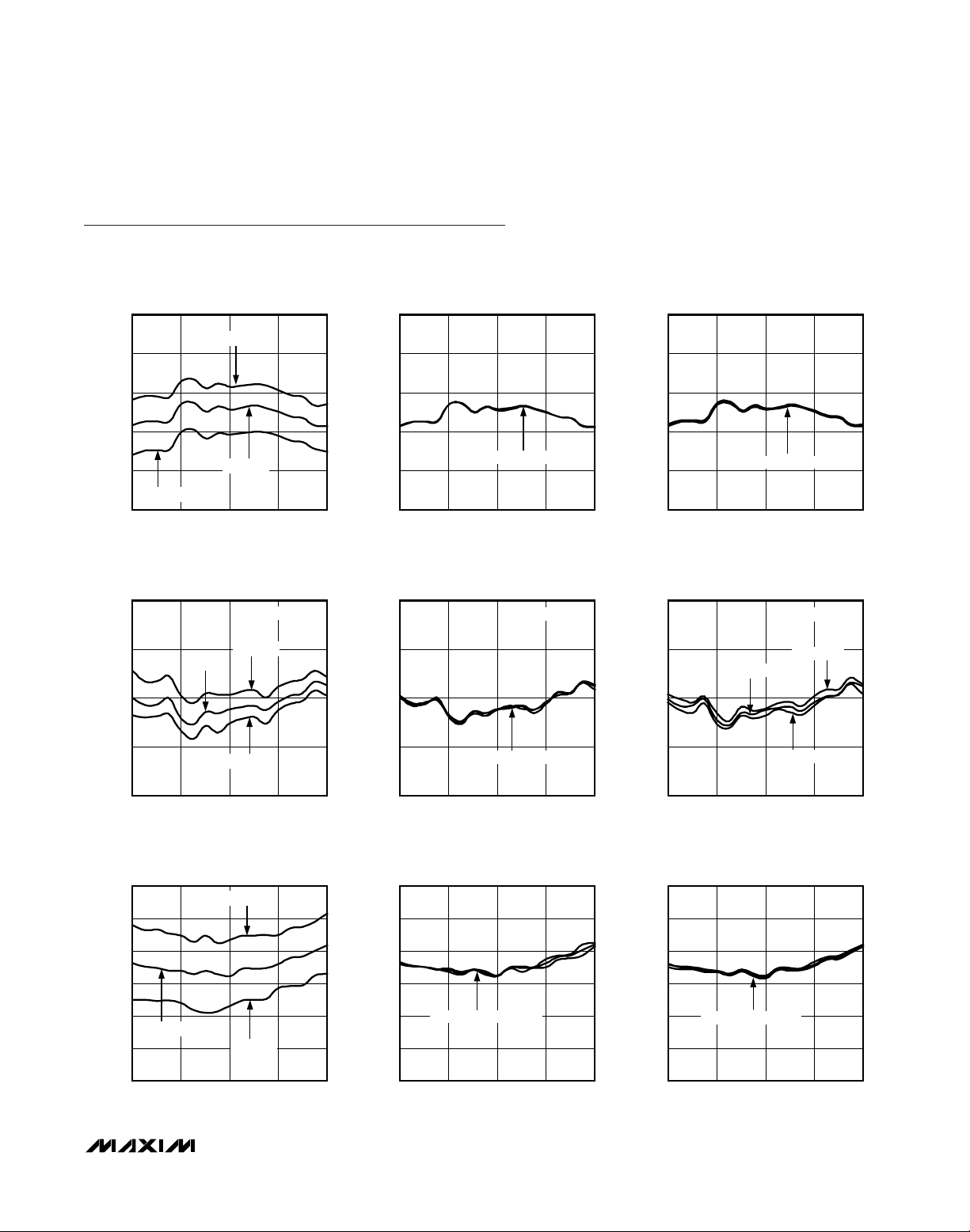
Typical Operating Characteristics
(
Typical Application Circuit
, standard RF band (see Table 1), VCC= +5.0V, LO is high-side injected for a 350MHz IF, PLO= 0dBm,
P
RF
= -5dBm, TC= +25°C, unless otherwise noted.)
CONVERSION GAIN vs. RF FREQUENCY
(LO > RF, STANDARD RF BAND)
MAX19997A toc01
RF FREQUENCY (MHz)
CONVERSION GAIN (dB)
280026002400
7
8
9
10
11
6
2200 3000
TC = -30°C
TC = +25°C
TC = +85°C
CONVERSION GAIN vs. RF FREQUENCY
(LO > RF, STANDARD RF BAND)
MAX19997A toc02
RF FREQUENCY (MHz)
CONVERSION GAIN (dB)
280026002400
7
8
9
10
11
6
2200 3000
PLO = -3dBm, 0dBm, +3dBm
CONVERSION GAIN vs. RF FREQUENCY
(LO > RF, STANDARD RF BAND)
MAX19997A toc03
RF FREQUENCY (MHz)
CONVERSION GAIN (dB)
280026002400
7
8
9
10
11
6
2200 3000
VCC = 4.75V, 5.0V, 5.25V
INPUT IP3 vs. RF FREQUENCY
(LO > RF, STANDARD RF BAND)
MAX19997A toc04
INPUT IP3 (dBm)
23
24
25
26
22
RF FREQUENCY (MHz)
2800260024002200 3000
TC = -30°C
PRF = -5dBm/TONE
TC = +25°C
TC = +85°C
INPUT IP3 vs. RF FREQUENCY
(LO > RF, STANDARD RF BAND)
MAX19997A toc05
INPUT IP3 (dBm)
23
24
25
26
22
RF FREQUENCY (MHz)
2800260024002200 3000
PRF = -5dBm/TONE
PLO = -3dBm, 0dBm, +3dBm
INPUT IP3 vs. RF FREQUENCY
(LO > RF, STANDARD RF BAND)
MAX19997A toc06
INPUT IP3 (dBm)
23
24
25
26
22
RF FREQUENCY (MHz)
2800260024002200 3000
PRF = -5dBm/TONE
VCC = 5.25V
VCC = 5.0V
VCC = 4.75V
NOISE FIGURE vs. RF FREQUENCY
(LO > RF, STANDARD RF BAND)
MAX19997A toc07
NOISE FIGURE (dB)
8
9
10
11
12
13
7
RF FREQUENCY (MHz)
2800260024002200 3000
TC = -30°C
TC = +25°C
TC = +85°C
NOISE FIGURE vs. RF FREQUENCY
(LO > RF, STANDARD RF BAND)
MAX19997A toc08
NOISE FIGURE (dB)
8
9
10
11
12
13
7
RF FREQUENCY (MHz)
2800260024002200 3000
PLO = -3dBm, 0dBm, +3dBm
NOISE FIGURE vs. RF FREQUENCY
(LO > RF, STANDARD RF BAND)
MAX19997A toc09
NOISE FIGURE (dB)
8
9
10
11
12
13
7
RF FREQUENCY (MHz)
2800260024002200 3000
VCC = 4.75V, 5.0V, 5.25V
MAX19997A
Dual, SiGe High-Linearity, 1800MHz to 2900MHz
Downconversion Mixer with LO Buffer
10 ______________________________________________________________________________________
Typical Operating Characteristics (continued)
(
Typical Application Circuit
, standard RF band (see Table 1), VCC= +5.0V, LO is high-side injected for a 350MHz IF, PLO= 0dBm,
P
RF
= -5dBm, TC= +25°C, unless otherwise noted.)
2LO - 2RF RESPONSE vs. RF FREQUENCY
(LO > RF, STANDARD RF BAND)
MAX19997A toc10
2LO - 2RF RESPONSE (dBc)
60
70
80
50
RF FREQUENCY (MHz)
2800260024002200 3000
TC = -30°C
PRF = -5dBm
TC = +25°C
TC = +85°C
2LO - 2RF RESPONSE vs. RF FREQUENCY
(LO > RF, STANDARD RF BAND)
MAX19997A toc11
2LO - 2RF RESPONSE (dBc)
60
70
80
50
RF FREQUENCY (MHz)
2800260024002200 3000
PLO = +3dBm
PRF = -5dBm
PLO = 0dBm
PLO = -3dBm
2LO - 2RF RESPONSE vs. RF FREQUENCY
(LO > RF, STANDARD RF BAND)
MAX19997A toc12
2LO - 2RF RESPONSE (dBc)
60
70
80
50
RF FREQUENCY (MHz)
2800260024002200 3000
VCC = 4.75V, 5.0V, 5.25V
PRF = -5dBm
3LO - 3RF RESPONSE vs. RF FREQUENCY
(LO > RF, STANDARD RF BAND)
MAX19997A toc13
3LO - 3RF RESPONSE (dBc)
65
75
85
95
55
RF FREQUENCY (MHz)
2800260024002200 3000
TC = -30°C
TC = +25°C, +85°C
PRF = -5dBm
3LO - 3RF RESPONSE vs. RF FREQUENCY
(LO > RF, STANDARD RF BAND)
MAX19997A toc14
3LO - 3RF RESPONSE (dBc)
65
75
85
95
55
RF FREQUENCY (MHz)
2800260024002200 3000
PLO = -3dBm, 0dBm, +3dBm
PRF = -5dBm
3LO - 3RF RESPONSE vs. RF FREQUENCY
(LO > RF, STANDARD RF BAND)
MAX19997A toc15
3LO - 3RF RESPONSE (dBc)
65
75
85
95
55
RF FREQUENCY (MHz)
2800260024002200 3000
VCC = 4.75V, 5.0V, 5.25V
PRF = -5dBm
INPUT P
1dB
vs. RF FREQUENCY
(LO > RF, STANDARD RF BAND)
MAX19997A toc16
INPUT P
1dB
(dBm)
10
11
12
13
9
RF FREQUENCY (MHz)
2800260024002200 3000
TC = -30°C
TC = +25°C
TC = +85°C
INPUT P
1dB
vs. RF FREQUENCY
(LO > RF, STANDARD RF BAND)
MAX19997A toc17
INPUT P
1dB
(dBm)
10
11
12
13
9
RF FREQUENCY (MHz)
2800260024002200 3000
PLO = -3dBm, 0dBm, +3dBm
INPUT P
1dB
vs. RF FREQUENCY
(LO > RF, STANDARD RF BAND)
MAX19997A toc18
INPUT P
1dB
(dBm)
10
11
12
13
9
RF FREQUENCY (MHz)
2800260024002200 3000
VCC = 4.75V
VCC = 5.25V
VCC = 5.0V
MAX19997A
Dual, SiGe High-Linearity, 1800MHz to 2900MHz
Downconversion Mixer with LO Buffer
______________________________________________________________________________________
11
Typical Operating Characteristics (continued)
(
Typical Application Circuit
, standard RF band (see Table 1), VCC= +5.0V, LO is high-side injected for a 350MHz IF, PLO= 0dBm,
P
RF
= -5dBm, TC= +25°C, unless otherwise noted.)
CHANNEL ISOLATION vs. RF FREQUENCY
(LO > RF, STANDARD RF BAND)
MAX19997A toc19
CHANNEL ISOLATION (dB)
35
40
45
50
55
60
30
RF FREQUENCY (MHz)
2800260024002200 3000
TC = -30°C, +25°C, +85°C
CHANNEL ISOLATION vs. RF FREQUENCY
(LO > RF, STANDARD RF BAND)
MAX19997A toc20
CHANNEL ISOLATION (dB)
35
40
45
50
55
60
30
RF FREQUENCY (MHz)
2800260024002200 3000
PLO = -3dBm, 0dBm, +3dBm
CHANNEL ISOLATION vs. RF FREQUENCY
(LO > RF, STANDARD RF BAND)
MAX19997A toc21
CHANNEL ISOLATION (dB)
35
40
45
50
55
60
30
RF FREQUENCY (MHz)
2800260024002200 3000
VCC = 4.75V, 5.0V, 5.25V
LO LEAKAGE AT IF PORT vs. LO FREQUENCY
(LO > RF, STANDARD RF BAND)
MAX19997A toc22
LO LEAKAGE AT IF PORT (dBm)
-30
-20
-10
0
-40
LO FREQUENCY (MHz)
3150295027502550 3350
TC = -30°C
TC = +25°C, +85°C
LO LEAKAGE AT IF PORT vs. LO FREQUENCY
(LO > RF, STANDARD RF BAND)
MAX19997A toc23
LO LEAKAGE AT IF PORT (dBm)
-30
-20
-10
0
-40
LO FREQUENCY (MHz)
3150295027502550 3350
PLO = -3dBm, 0dBm, +3dBm
LO LEAKAGE AT IF PORT vs. LO FREQUENCY
(LO > RF, STANDARD RF BAND)
MAX19997A toc24
LO LEAKAGE AT IF PORT (dBm)
-30
-20
-10
0
-40
LO FREQUENCY (MHz)
3150295027502550 3350
VCC = 4.75V, 5.0V, 5.25V
RF-TO-IF ISOLATION vs. RF FREQUENCY
(LO > RF, STANDARD RF BAND)
MAX19997A toc25
RF-TO-IF ISOLATION (dB)
20
30
40
10
RF FREQUENCY (MHz)
2800260024002200 3000
TC = -30°C
TC = +25°C
TC = +85°C
RF-TO-IF ISOLATION vs. RF FREQUENCY
(LO > RF, STANDARD RF BAND)
MAX19997A toc26
RF-TO-IF ISOLATION (dB)
20
30
40
10
RF FREQUENCY (MHz)
2800260024002200 3000
PLO = -3dBm, 0dBm, +3dBm
RF-TO-IF ISOLATION vs. RF FREQUENCY
(LO > RF, STANDARD RF BAND)
MAX19997A toc27
RF-TO-IF ISOLATION (dB)
20
30
40
10
RF FREQUENCY (MHz)
2800260024002200 3000
VCC = 4.75V, 5.0V, 5.25V

MAX19997A
Dual, SiGe High-Linearity, 1800MHz to 2900MHz
Downconversion Mixer with LO Buffer
12 ______________________________________________________________________________________
Typical Operating Characteristics (continued)
(
Typical Application Circuit
, standard RF band (see Table 1), VCC= +5.0V, LO is high-side injected for a 350MHz IF, PLO= 0dBm,
P
RF
= -5dBm, TC= +25°C, unless otherwise noted.)
LO LEAKAGE AT RF PORT vs. LO FREQUENCY
(LO > RF, STANDARD RF BAND)
MAX19997A toc28
LO FREQUENCY (MHz)
LO LEAKAGE AT RF PORT (dBm)
3180296027402520
-40
-30
-20
-10
-50
2300 3400
TC = -30°C, +25°C, +85°C
LO LEAKAGE AT RF PORT vs. LO FREQUENCY
(LO > RF, STANDARD RF BAND)
MAX19997A toc29
LO FREQUENCY (MHz)
LO LEAKAGE AT RF PORT (dBm)
3180296027402520
-40
-30
-20
-10
-50
2300 3400
P
LO
= -3dBm, 0dBm, +3dBm
LO LEAKAGE AT RF PORT vs. LO FREQUENCY
(LO > RF, STANDARD RF BAND)
MAX19997A toc30
LO FREQUENCY (MHz)
LO LEAKAGE AT RF PORT (dBm)
3180296027402520
-40
-30
-20
-10
-50
2300 3400
VCC = 4.75V, 5.0V, 5.25V
2LO LEAKAGE AT RF PORT vs. LO FREQUENCY
(LO > RF, STANDARD RF BAND)
MAX19997A toc31
LO FREQUENCY (MHz)
2LO LEAKAGE AT RF PORT (dBm)
3180296027402520
-40
-30
-20
-10
-50
2300 3400
TC = -30°C, +25°C, +85°C
2LO LEAKAGE AT RF PORT vs. LO FREQUENCY
(LO > RF, STANDARD RF BAND)
MAX19997A toc32
LO FREQUENCY (MHz)
2LO LEAKAGE AT RF PORT (dBm)
3180296027402520
-40
-30
-20
-10
-50
2300 3400
P
LO
= -3dBm, 0dBm, +3dBm
2LO LEAKAGE AT RF PORT vs. LO FREQUENCY
(LO > RF, STANDARD RF BAND)
MAX19997A toc33
LO FREQUENCY (MHz)
2LO LEAKAGE AT RF PORT (dBm)
3180296027402520
-40
-30
-20
-10
-50
2300 3400
VCC = 4.75V, 5.0V, 5.25V

MAX19997A
Dual, SiGe High-Linearity, 1800MHz to 2900MHz
Downconversion Mixer with LO Buffer
______________________________________________________________________________________
13
Typical Operating Characteristics (continued)
(
Typical Application Circuit
, standard RF band (see Table 1), VCC= +5.0V, LO is high-side injected for a 350MHz IF, PLO= 0dBm,
P
RF
= -5dBm, TC= +25°C, unless otherwise noted.)
LO PORT RETURN LOSS vs. LO FREQUENCY
(LO > RF, STANDARD RF BAND)
MAX19997A toc37
LO FREQUENCY (MHz)
LO PORT RETURN LOSS (dB)
31502900265024002150
20
15
10
5
0
25
1900 3400
PLO = +3dBm
PLO = 0dBm
PLO = -3dBm
SUPPLY CURRENT vs. TEMPERATURE (TC)
(LO > RF, STANDARD RF BAND)
MAX19997A toc38
TEMPERATURE (°C)
SUPPLY CURRENT (mA)
6545255-15
360
370
380
390
400
350
-35 85
VCC = 5.25V
VCC = 5.0V
VCC = 4.75V
RF PORT RETURN LOSS vs. RF FREQUENCY
(LO > RF, STANDARD RF BAND)
MAX19997A toc34
RF PORT RETURN LOSS (dB)
25
20
15
10
5
0
30
RF FREQUENCY (MHz)
2800260024002200 3000
PLO = -3dBm, 0dBm, +3dBm
fIF = 350MHz
IF PORT RETURN LOSS vs. IF FREQUENCY
(LO > RF, STANDARD RF BAND)
MAX19997A toc35
IF FREQUENCY (MHz)
IF PORT RETURN LOSS (dB)
410320230140
25
20
15
10
5
0
30
50 500
VCC = 4.75V, 5.0V, 5.25V
fLO = 2600MHz
IF PORT RETURN LOSS vs. IF FREQUENCY
(LO > RF, STANDARD RF BAND)
MAX19997A toc36
IF FREQUENCY (MHz)
IF PORT RETURN LOSS (dB)
410320230140
25
20
15
10
5
0
30
50 500
fLO = 2600MHz
fLO = 2950MHz
fLO = 2350MHz

MAX19997A
Dual, SiGe High-Linearity, 1800MHz to 2900MHz
Downconversion Mixer with LO Buffer
14 ______________________________________________________________________________________
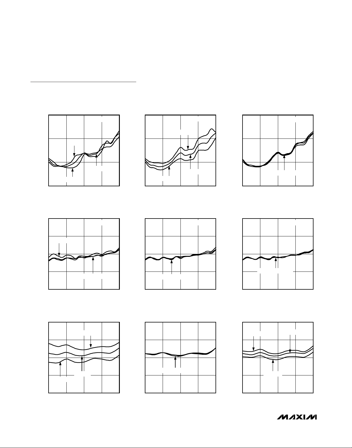
Typical Operating Characteristics (continued)
(
Typical Application Circuit
, extended RF band (see Table 2), VCC= +5.0V, LO is high-side injected for a 350MHz IF, PLO= 0dBm,
P
RF
= -5dBm, TC= +25°C, unless otherwise noted.)
INPUT IP3 vs. RF FREQUENCY
(LO > RF, EXTENDED RF BAND)
MAX19997A toc42
RF FREQUENCY (MHz)
INPUT IP3 (dBm)
2200210020001900
23
24
25
26
22
1800 2300
TC = -30°C
PRF = -5dBm/TONE
TC = +25°C
TC = +85°C
INPUT IP3 vs. RF FREQUENCY
(LO > RF, EXTENDED RF BAND)
MAX19997A toc43
RF FREQUENCY (MHz)
INPUT IP3 (dBm)
2200210020001900
23
24
25
26
22
1800 2300
PRF = -5dBm/TONE
PLO = -3dBm, 0dBm, +3dBm
INPUT IP3 vs. RF FREQUENCY
(LO > RF, EXTENDED RF BAND)
MAX19997A toc44
RF FREQUENCY (MHz)
INPUT IP3 (dBm)
2200210020001900
23
24
25
26
22
1800 2300
PRF = -5dBm/TONE
VCC = 4.75V
VCC = 5.25V
VCC = 5.0V
CONVERSION GAIN vs. RF FREQUENCY
(LO > RF, EXTENDED RF BAND)
11
10
9
8
CONVERSION GAIN (dB)
7
6
TC = +85°C
1800 2300
RF FREQUENCY (MHz)
TC = -30°C
TC = +25°C
CONVERSION GAIN vs. RF FREQUENCY
(LO > RF, EXTENDED RF BAND)
11
10
MAX19997A toc39
9
8
CONVERSION GAIN (dB)
7
6
2200210020001900
1800 2300
PLO = -3dBm, 0dBm, +3dBm
2200210020001900
RF FREQUENCY (MHz)
MAX19997A toc40
CONVERSION GAIN vs. RF FREQUENCY
(LO > RF, EXTENDED RF BAND)
11
10
9
8
CONVERSION GAIN (dB)
7
6
1800 2300
VCC = 4.75V, 5.0V, 5.25V
RF FREQUENCY (MHz)
MAX19997A toc41
2200210020001900
NOISE FIGURE vs. RF FREQUENCY
(LO > RF, EXTENDED RF BAND)
13
12
11
10
NOISE FIGURE (dB)
9
TC = +25°C
8
7
1800 2300
TC = +85°C
TC = -30°C
RF FREQUENCY (MHz)
NOISE FIGURE vs. RF FREQUENCY
(LO > RF, EXTENDED RF BAND)
13
12
MAX19997A toc45
11
10
NOISE FIGURE (dB)
9
8
2200210020001900
7
1800 2300
PLO = -3dBm, 0dBm, +3dBm
2200210020001900
RF FREQUENCY (MHz)
MAX19997A toc46
NOISE FIGURE vs. RF FREQUENCY
(LO > RF, EXTENDED RF BAND)
13
12
11
10
NOISE FIGURE (dB)
9
8
7
1800 2300
VCC = 4.75V, 5.0V, 5.25V
RF FREQUENCY (MHz)
MAX19997A toc47
2200210020001900

MAX19997A
Dual, SiGe High-Linearity, 1800MHz to 2900MHz
Downconversion Mixer with LO Buffer
______________________________________________________________________________________
15
Typical Operating Characteristics (continued)
(
Typical Application Circuit
, extended RF band (see Table 2), VCC= +5.0V, LO is high-side injected for a 350MHz IF, PLO= 0dBm,
P
RF
= -5dBm, TC= +25°C, unless otherwise noted.)
2LO - 2RF RESPONSE vs. RF FREQUENCY
(LO > RF, EXTENDED RF BAND)
70
TC = +85°C
60
50
2LO - 2RF RESPONSE (dBc)
40
TC = -30°C
1800 2300
RF FREQUENCY (MHz)
PRF = -5dBm
TC = +25°C
2200210020001900
3LO - 3RF RESPONSE vs. RF FREQUENCY
(LO > RF, EXTENDED RF BAND)
95
85
TC = -30°C
PRF = -5dBm
2LO - 2RF RESPONSE vs. RF FREQUENCY
70
MAX19997A toc48
60
50
2LO - 2RF RESPONSE (dBc)
40
1800 2300
3LO - 3RF RESPONSE vs. RF FREQUENCY
95
MAX19997A toc51
85
(LO > RF, EXTENDED RF BAND)
PRF = -5dBm
MAX19997A toc49
PLO = -3dBm, 0dBm, +3dBm
2200210020001900
RF FREQUENCY (MHz)
(LO > RF, EXTENDED RF BAND)
PRF = -5dBm
MAX19997A toc52
2LO - 2RF RESPONSE vs. RF FREQUENCY
(LO > RF, EXTENDED RF BAND)
70
60
50
2LO - 2RF RESPONSE (dBc)
40
1800 2300
VCC = 4.75V, 5.0V, 5.25V
RF FREQUENCY (MHz)
3LO - 3RF RESPONSE vs. RF FREQUENCY
(LO > RF, EXTENDED RF BAND)
95
85
PRF = -5dBm
MAX19997A toc50
2200210020001900
PRF = -5dBm
MAX19997A toc53
75
3LO - 3RF RESPONSE (dBc)
65
TC = +25°C, +85°C
55
1800 2300
RF FREQUENCY (MHz)
INPUT P
vs. RF FREQUENCY
1dB
(LO > RF, EXTENDED RF BAND)
13
12
(dBm)
1dB
11
INPUT P
10
9
1800 2300
TC = +85°C
TC = -30°C
RF FREQUENCY (MHz)
TC = +25°C
75
3LO - 3RF RESPONSE (dBc)
65
2200210020001900
55
1800 2300
PLO = -3dBm, 0dBm, +3dBm
RF FREQUENCY (MHz)
INPUT P
vs. RF FREQUENCY
1dB
2200210020001900
(LO > RF, EXTENDED RF BAND)
13
MAX19997A toc54
12
(dBm)
1dB
11
INPUT P
10
2200210020001900
9
1800 2300
PLO = -3dBm, 0dBm, +3dBm
2200210020001900
RF FREQUENCY (MHz)
75
3LO - 3RF RESPONSE (dBc)
65
55
1800 2300
13
MAX19997A toc55
12
(dBm)
1dB
11
INPUT P
10
9
1800 2300
VCC = 4.75V, 5.0V, 5.25V
RF FREQUENCY (MHz)
INPUT P
vs. RF FREQUENCY
1dB
(LO > RF, EXTENDED RF BAND)
VCC = 5.0V
VCC = 4.75V
RF FREQUENCY (MHz)
VCC = 5.25V
2200210020001900
MAX19997A toc56
2200210020001900

MAX19997A
Dual, SiGe High-Linearity, 1800MHz to 2900MHz
Downconversion Mixer with LO Buffer
16 ______________________________________________________________________________________
Typical Operating Characteristics (continued)
(
Typical Application Circuit
, extended RF band (see Table 2), VCC= +5.0V, LO is high-side injected for a 350MHz IF, PLO= 0dBm,
P
RF
= -5dBm, TC= +25°C, unless otherwise noted.)
LO LEAKAGE AT IF PORT vs. LO FREQUENCY
(LO > RF, EXTENDED RF BAND)
MAX19997A toc61
LO FREQUENCY (MHz)
LO LEAKAGE AT IF PORT (dBm)
2550245023502250
-20
-10
0
-30
2150 2650
PLO = -3dBm, 0dBm, +3dBm
CHANNEL ISOLATION vs. RF FREQUENCY
(LO > RF, EXTENDED RF BAND)
60
55
50
45
40
CHANNEL ISOLATION (dB)
35
30
1800 2300
TC = -30°C, +25°C, +85°C
RF FREQUENCY (MHz)
LO LEAKAGE AT IF PORT vs. LO FREQUENCY
(LO > RF, EXTENDED RF BAND)
0
-10
-20
LO LEAKAGE AT IF PORT (dBm)
TC = -30°C, +25°C, +85°C
CHANNEL ISOLATION vs. RF FREQUENCY
(LO > RF, EXTENDED RF BAND)
60
55
MAX19997A toc57
50
45
40
CHANNEL ISOLATION (dB)
35
30
2200210020001900
1800 2300
PLO = -3dBm, 0dBm, +3dBm
2200210020001900
RF FREQUENCY (MHz)
MAX19997A toc58
CHANNEL ISOLATION vs. RF FREQUENCY
(LO > RF, EXTENDED RF BAND)
60
55
50
45
40
CHANNEL ISOLATION (dB)
35
30
1800 2300
VCC = 4.75V, 5.0V, 5.25V
RF FREQUENCY (MHz)
MAX19997A toc59
2200210020001900
LO LEAKAGE AT IF PORT vs. LO FREQUENCY
(LO > RF, EXTENDED RF BAND)
0
MAX19997A toc60
-10
-20
LO LEAKAGE AT IF PORT (dBm)
VCC = 4.75V, 5.0V, 5.25V
MAX19997A toc62
-30
2150 2650
LO FREQUENCY (MHz)
RF-TO-IF ISOLATION vs. RF FREQUENCY
(LO > RF, EXTENDED RF BAND)
30
20
RF-TO-IF ISOLATION (dB)
10
TC = +25°C
1800 2300
RF FREQUENCY (MHz)
TC = +85°C
TC = -30°C
2550245023502250
RF-TO-IF ISOLATION vs. RF FREQUENCY
(LO > RF, EXTENDED RF BAND)
30
MAX19997A toc63
20
RF-TO-IF ISOLATION (dB)
2200210020001900
10
1800 2300
PLO = -3dBm, 0dBm, +3dBm
2200210020001900
RF FREQUENCY (MHz)
-30
2150 2650
30
MAX19997A toc64
20
RF-TO-IF ISOLATION (dB)
10
1800 2300
2550245023502250
LO FREQUENCY (MHz)
RF-TO-IF ISOLATION vs. RF FREQUENCY
(LO > RF, EXTENDED RF BAND)
VCC = 4.75V, 5.0V, 5.25V
2200210020001900
RF FREQUENCY (MHz)
MAX19997A toc65

MAX19997A
Dual, SiGe High-Linearity, 1800MHz to 2900MHz
Downconversion Mixer with LO Buffer
______________________________________________________________________________________
17
Typical Operating Characteristics (continued)
(
Typical Application Circuit
, extended RF band (see Table 2), VCC= +5.0V, LO is high-side injected for a 350MHz IF, PLO= 0dBm,
P
RF
= -5dBm, TC= +25°C, unless otherwise noted.)
LO LEAKAGE AT RF PORT vs. LO FREQUENCY
(LO > RF, EXTENDED RF BAND)
MAX19997A toc66
LO LEAKAGE AT RF PORT (dBm)
3180296027402520
-30
-40
-20
-10
-50
2300
3400
LO FREQUENCY (MHz)
TC = -30°C, +25°C, +85°C
Y
Y
Y
2LO LEAKAGE AT RF PORT vs. LO FREQUENC
(LO > RF, EXTENDED RF BAND)
-10
-20
TC = -30°C, +25°C, +85°C
LO LEAKAGE AT RF PORT vs. LO FREQUENCY
-10
-20
-30
-40
LO LEAKAGE AT RF PORT (dBm)
-50
2300
2LO LEAKAGE AT RF PORT vs. LO FREQUENC
-10
MAX19997A toc69
-20
(LO > RF, EXTENDED RF BAND)
PLO = -3dBm, 0dBm, +3dBm
3180296027402520
LO FREQUENCY (MHz)
(LO > RF, EXTENDED RF BAND)
PLO = -3dBm, 0dBm, +3dBm
MAX19997A toc67
3400
MAX19997A toc70
LO LEAKAGE AT RF PORT vs. LO FREQUENCY
(LO > RF, EXTENDED RF BAND)
-10
-20
-30
-40
LO LEAKAGE AT RF PORT (dBm)
-50
2300
VCC = 4.75V, 5.0V, 5.25V
LO FREQUENCY (MHz)
2LO LEAKAGE AT RF PORT vs. LO FREQUENC
(LO > RF, EXTENDED RF BAND)
-10
-20
VCC = 4.75V, 5.0V, 5.25V
MAX19997A toc68
3180296027402520
3400
MAX19997A toc71
-30
-40
2LO LEAKAGE AT RF PORT (dBm)
-50
2300 3400
LO FREQUENCY (MHz)
-30
-40
2LO LEAKAGE AT RF PORT (dBm)
3180296027402520
-50
2300
LO FREQUENCY (MHz)
3180296027402520
3400
-30
-40
2LO LEAKAGE AT RF PORT (dBm)
-50
2300
LO FREQUENCY (MHz)
3180296027402520
3400

MAX19997A
Dual, SiGe High-Linearity, 1800MHz to 2900MHz
Downconversion Mixer with LO Buffer
18 ______________________________________________________________________________________
Typical Operating Characteristics (continued)
(
Typical Application Circuit
, extended RF band (see Table 2), VCC= +5.0V, LO is high-side injected for a 350MHz IF, PLO= 0dBm,
P
RF
= -5dBm, TC= +25°C, unless otherwise noted.)
IF PORT RETURN LOSS vs. IF FREQUENCY
(LO > RF, EXTENDED RF BAND)
MAX19997A toc73
IF PORT RETURN LOSS (dB)
410320230140
15
10
25
20
5
0
30
50 500
IF FREQUENCY (MHz)
fLO = 2600MHz
VCC = 4.75V, 5.0V, 5.25V
RF PORT RETURN LOSS vs. RF FREQUENCY
(LO > RF, EXTENDED RF BAND)
0
5
10
15
20
RF PORT RETURN LOSS (dB)
25
30
1800 2300
PLO = -3dBm, 0dBm, +3dBm
RF FREQUENCY (MHz)
LO PORT RETURN LOSS vs. LO FREQUENCY
0
5
10
15
LO PORT RETURN LOSS (dB)
20
fIF = 350MHz
MAX19997A toc72
2200210020001900
(LO > RF, EXTENDED RF BAND)
PLO = +3dBm
PLO = -3dBm
PLO = 0dBm
MAX19997A toc75
SUPPLY CURRENT (mA)
IF PORT RETURN LOSS vs. IF FREQUENCY
0
5
10
15
20
IF PORT RETURN LOSS (dB)
25
30
50 500
SUPPLY CURRENT vs. TEMPERATURE (TC)
(LO > RF, EXTENDED RF BAND)
400
VCC = 5.25V
390
380
370
VCC = 5.0V
360
VCC = 4.75V
(LO > RF, EXTENDED RF BAND)
MAX19997A toc74
fLO = 2350MHz
fLO = 2600MHz
fLO = 2950MHz
410320230140
IF FREQUENCY (MHz)
MAX19997A toc76
25
1900 3400
LO FREQUENCY (MHz)
350
2900 3150265024002150
-35
TEMPERATURE (°C)
45 65255-15
85

MAX19997A
Dual, SiGe High-Linearity, 1800MHz to 2900MHz
Downconversion Mixer with LO Buffer
______________________________________________________________________________________
19
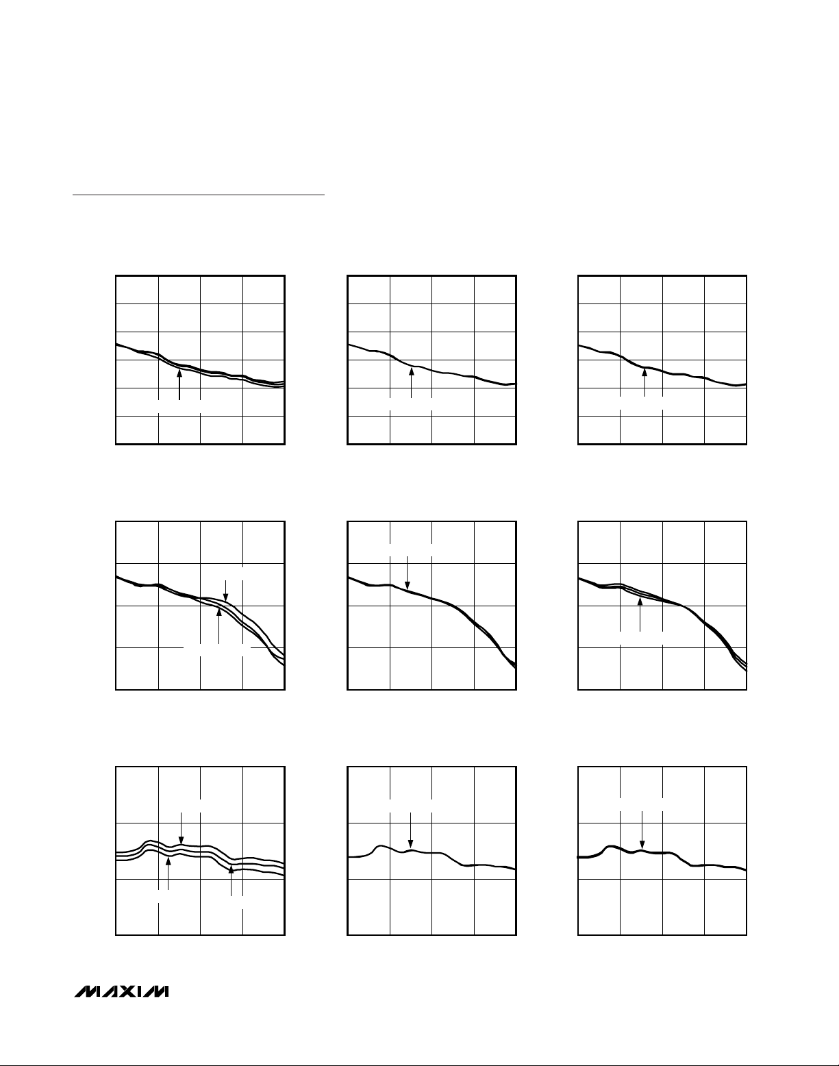
Typical Operating Characteristics (continued)
(
Typical Application Circuit
, standard RF band (see Table 1), VCC= +5.0V, LO is low-side injected for a 350MHz IF, PLO= 0dBm,
P
RF
= -5dBm, TC= +25°C, unless otherwise noted.)
NOISE FIGURE vs. RF FREQUENCY
(RF > LO, STANDARD RF BAND)
MAX19997A toc84
NOISE FIGURE (dB)
280026002400
8
9
10
11
12
13
7
2200 3000
RF FREQUENCY (MHz)
PLO = -3dBm, 0dBm, +3dBm
CONVERSION GAIN vs. RF FREQUENCY
(RF > LO, STANDARD RF BAND)
11
TC = -30°C
10
9
8
CONVERSION GAIN (dB)
7
6
TC = +85°C
2200 3000
RF FREQUENCY (MHz)
TC = +25°C
280026002400
INPUT IP3 vs. RF FREQUENCY
(RF > LO, STANDARD RF BAND)
26
TC = +85°C
25
PRF = -5dBm/TONE
TC = +25°C
11
10
MAX19997A toc77
9
8
CONVERSION GAIN (dB)
7
6
26
MAX19997A toc80
25
CONVERSION GAIN vs. RF FREQUENCY
(RF > LO, STANDARD RF BAND)
PLO = -3dBm, 0dBm, +3dBm
2200 3000
RF FREQUENCY (MHz)
280026002400
INPUT IP3 vs. RF FREQUENCY
(RF > LO, STANDARD RF BAND)
PRF = -5dBm/TONE
PLO = -3dBm, 0dBm, +3dBm
MAX19997A toc78
MAX19997A toc81
CONVERSION GAIN vs. RF FREQUENCY
(RF > LO, STANDARD RF BAND)
11
10
9
8
CONVERSION GAIN (dB)
7
6
2200 3000
VCC = 4.75V, 5.0V, 5.25V
RF FREQUENCY (MHz)
INPUT IP3 vs. RF FREQUENCY
(RF > LO, STANDARD RF BAND)
26
25
PRF = -5dBm/TONE
MAX19997A toc79
280026002400
MAX19997A toc82
24
INPUT IP3 (dBm)
23
22
13
12
11
10
NOISE FIGURE (dB)
9
8
7
TC = -30°C
2200 3000
RF FREQUENCY (MHz)
280026002400
NOISE FIGURE vs. RF FREQUENCY
(RF > LO, STANDARD RF BAND)
TC = +85°C
TC = +25°C
2200 3000
RF FREQUENCY (MHz)
TC = -30°C
280026002400
INPUT IP3 (dBm)
MAX19997A toc83
24
23
22
2200 3000
RF FREQUENCY (MHz)
280026002400
24
INPUT IP3 (dBm)
23
22
VCC = 4.75V, 5.0V, 5.25V
2200 3000
RF FREQUENCY (MHz)
280026002400
NOISE FIGURE vs. RF FREQUENCY
(RF > LO, STANDARD RF BAND)
13
12
11
10
NOISE FIGURE (dB)
9
8
7
2200 3000
VCC = 4.75V, 5.0V, 5.25V
280026002400
RF FREQUENCY (MHz)
MAX19997A toc85

MAX19997A
Dual, SiGe High-Linearity, 1800MHz to 2900MHz
Downconversion Mixer with LO Buffer
20 ______________________________________________________________________________________
Typical Operating Characteristics (continued)
(
Typical Application Circuit
, standard RF band (see Table 1), VCC= +5.0V, LO is low-side injected for a 350MHz IF, PLO= 0dBm,
P
RF
= -5dBm, TC= +25°C, unless otherwise noted.)
2RF - 2LO RESPONSE vs. RF FREQUENCY
(RF > LO, STANDARD RF BAND)
80
70
TC = +85°C
60
2RF - 2LO RESPONSE (dBc)
50
95
85
75
3RF - 3LO RESPONSE (dBc)
65
TC = -30°C
2200 3000
RF FREQUENCY (MHz)
3RF - 3LO RESPONSE vs. RF FREQUENCY
(RF > LO, STANDARD RF BAND)
TC = -30°C, +25°C, +85°C
PRF = -5dBm
TC = +25°C
280026002400
PRF = -5dBm
2RF - 2LO RESPONSE vs. RF FREQUENCY
80
MAX19997A toc86
70
60
2RF - 2LO RESPONSE (dBc)
50
2200 3000
3RF - 3LO RESPONSE vs. RF FREQUENCY
95
MAX19997A toc89
85
75
3RF - 3LO RESPONSE (dBc)
65
(RF > LO, STANDARD RF BAND)
PRF = -5dBm
PLO = 0dBm
PLO = +3dBm
PLO = -3dBm
280026002400
RF FREQUENCY (MHz)
(RF > LO, STANDARD RF BAND)
PRF = -5dBm
PLO = -3dBm, 0dBm, +3dBm
2RF - 2LO RESPONSE vs. RF FREQUENCY
80
MAX19997A toc87
70
60
2RF - 2LO RESPONSE (dBc)
50
2200 3000
3RF - 3LO RESPONSE vs. RF FREQUENCY
95
MAX19997A toc90
85
75
3RF - 3LO RESPONSE (dBc)
65
(RF > LO, STANDARD RF BAND)
PRF = -5dBm
MAX19997A toc88
VCC = 4.75V, 5.0V, 5.25V
280026002400
RF FREQUENCY (MHz)
(RF > LO, STANDARD RF BAND)
PRF = -5dBm
MAX19997A toc91
VCC = 4.75V, 5.0V, 5.25V
55
2200 3000
RF FREQUENCY (MHz)
INPUT P
vs. RF FREQUENCY
1dB
280026002400
(RF > LO, STANDARD RF BAND)
13
12
(dBm)
1dB
11
INPUT P
10
9
2200 3000
TC = +85°C
TC = -30°C
RF FREQUENCY (MHz)
TC = +25°C
280026002400
MAX19997A toc92
55
2200 3000
RF FREQUENCY (MHz)
INPUT P
vs. RF FREQUENCY
1dB
280026002400
(RF > LO, STANDARD RF BAND)
13
12
(dBm)
1dB
11
INPUT P
10
9
2200 3000
PLO = -3dBm, 0dBm, +3dBm
280026002400
RF FREQUENCY (MHz)
MAX19997A toc93
(dBm)
1dB
INPUT P
55
2200 3000
RF FREQUENCY (MHz)
INPUT P
1dB
(RF > LO, STANDARD RF BAND)
13
12
VCC = 5.0V
11
10
9
2200 3000
RF FREQUENCY (MHz)
280026002400
vs. RF FREQUENCY
VCC = 5.25V
VCC = 4.75V
280026002400
MAX19997A toc94

MAX19997A
Dual, SiGe High-Linearity, 1800MHz to 2900MHz
Downconversion Mixer with LO Buffer
______________________________________________________________________________________
21
Typical Operating Characteristics (continued)
(
Typical Application Circuit
, standard RF band (see Table 1), VCC= +5.0V, LO is low-side injected for a 350MHz IF, PLO= 0dBm,
P
RF
= -5dBm, TC= +25°C, unless otherwise noted.)
LO LEAKAGE AT IF PORT vs. LO FREQUENCY
(RF > LO, STANDARD RF BAND)
MAX19997A toc100
LO LEAKAGE AT IF PORT (dBm)
245022502050
-20
-10
0
-30
1850 2650
LO FREQUENCY (MHz)
VCC = 4.75V, 5.0V, 5.25V
CHANNEL ISOLATION vs. RF FREQUENCY
(RF > LO, STANDARD RF BAND)
55
50
45
40
CHANNEL ISOLATION (dB)
35
30
2200 3000
TC = -30°C, +25°C, +85°C
280026002400
RF FREQUENCY (MHz)
LO LEAKAGE AT IF PORT vs. LO FREQUENCY
(RF > LO, STANDARD RF BAND)
0
-10
55
50
MAX19997A toc95
45
40
CHANNEL ISOLATION (dB)
35
30
2200 3000
LO LEAKAGE AT IF PORT vs. LO FREQUENCY
0
MAX19997A toc98
-10
CHANNEL ISOLATION vs. RF FREQUENCY
(RF > LO, STANDARD RF BAND)
MAX19997A toc96
PLO = -3dBm, 0dBm, +3dBm
280026002400
RF FREQUENCY (MHz)
(RF > LO, STANDARD RF BAND)
MAX19997A toc99
CHANNEL ISOLATION vs. RF FREQUENCY
(RF > LO, STANDARD RF BAND)
55
50
45
40
CHANNEL ISOLATION (dB)
35
30
2200 3000
VCC = 4.75V, 5.0V, 5.25V
RF FREQUENCY (MHz)
MAX19997A toc97
280026002400
TC = -30°C, +25°C, +85°C
-20
LO LEAKAGE AT IF PORT (dBm)
-30
1850 2650
LO FREQUENCY (MHz)
RF-TO-IF ISOLATION vs. RF FREQUENCY
(RF > LO, STANDARD RF BAND)
30
TC = +85°C
20
TC = +25°C
RF-TO-IF ISOLATION (dB)
10
2200 3000
RF FREQUENCY (MHz)
PLO = -3dBm, 0dBm, +3dBm
-20
LO LEAKAGE AT IF PORT (dBm)
TC = -30°C
-30
245022502050
1850 2650
LO FREQUENCY (MHz)
RF-TO-IF ISOLATION vs. RF FREQUENCY
(RF > LO, STANDARD RF BAND)
30
MAX19997A toc101
20
RF-TO-IF ISOLATION (dB)
280026002400
PLO = -3dBm, 0dBm, +3dBm
10
2200 3000
RF FREQUENCY (MHz)
245022502050
RF-TO-IF ISOLATION vs. RF FREQUENCY
(RF > LO, STANDARD RF BAND)
30
MAX19997A toc102
20
VCC = 4.75V, 5.0V, 5.25V
RF-TO-IF ISOLATION (dB)
10
280026002400
2200 3000
RF FREQUENCY (MHz)
280026002400
MAX19997A toc103

MAX19997A
Dual, SiGe High-Linearity, 1800MHz to 2900MHz
Downconversion Mixer with LO Buffer
22 ______________________________________________________________________________________
Typical Operating Characteristics (continued)
(
Typical Application Circuit
, standard RF band (see Table 1), VCC= +5.0V, LO is low-side injected for a 350MHz IF, PLO= 0dBm,
P
RF
= -5dBm, TC= +25°C, unless otherwise noted.)
Y
Y
Y
LO LEAKAGE AT RF PORT vs. LO FREQUENCY
(RF > LO, STANDARD RF BAND)
-10
-20
-30
-40
LO LEAKAGE AT RF PORT (dBm)
-50
1900
TC = -30°C, +25°C, +85°C
LO FREQUENCY (MHz)
2LO LEAKAGE AT RF PORT vs. LO FREQUENC
(RF > LO, STANDARD RF BAND)
-10
-20
-30
-40
2LO LEAKAGE AT RF PORT (dBm)
TC = -30°C, +25°C, +85°C
LO LEAKAGE AT RF PORT vs. LO FREQUENCY
(RF > LO, STANDARD RF BAND)
-10
MAX19997A toc104
-20
-30
-40
LO LEAKAGE AT RF PORT (dBm)
2700250023002100
2900
-50
PLO = -3dBm, 0dBm, +3dBm
1900 2900
LO FREQUENCY (MHz)
2700250023002100
MAX19997A toc105
2LO LEAKAGE AT RF PORT vs. LO FREQUENC
(RF > LO, STANDARD RF BAND)
-10
MAX19997A toc107
-20
-30
-40
2LO LEAKAGE AT RF PORT (dBm)
PLO = -3dBm, 0dBm, +3dBm
MAX19997A toc108
LO LEAKAGE AT RF PORT vs. LO FREQUENCY
(RF > LO, STANDARD RF BAND)
-10
-20
-30
-40
LO LEAKAGE AT RF PORT (dBm)
-50
1900 2900
VCC = 4.75V, 5.0V, 5.25V
LO FREQUENCY (MHz)
2LO LEAKAGE AT RF PORT vs. LO FREQUENC
(RF > LO, STANDARD RF BAND)
-10
-20
-30
-40
2LO LEAKAGE AT RF PORT (dBm)
VCC = 4.75V, 5.0V, 5.25V
MAX19997A toc106
2700250023002100
MAX19997A toc109
-50
1900 2900
LO FREQUENCY (MHz)
2700250023002100
-50
1900 2900
LO FREQUENCY (MHz)
2700250023002100
-50
1900
LO FREQUENCY (MHz)
2700250023002100
2900

MAX19997A
Dual, SiGe High-Linearity, 1800MHz to 2900MHz
Downconversion Mixer with LO Buffer
______________________________________________________________________________________
23
Typical Operating Characteristics (continued)
(
Typical Application Circuit
, standard RF band (see Table 1), VCC= +5.0V, LO is low-side injected for a 350MHz IF, PLO= 0dBm,
P
RF
= -5dBm, TC= +25°C, unless otherwise noted.)
RF PORT RETURN LOSS vs. RF FREQUENCY
(RF > LO, STANDARD RF BAND)
0
5
10
15
20
RF PORT RETURN LOSS (dB)
PLO = -3dBm, 0dBm, +3dBm
25
30
2200 3000
RF FREQUENCY (MHz)
fIF = 350MHz
280026002400
LO PORT RETURN LOSS vs. LO FREQUENCY
(RF > LO, STANDARD RF BAND)
0
PLO = +3dBm
5
IF PORT RETURN LOSS vs. IF FREQUENCY
(RF > LO, STANDARD RF BAND)
0
5
fLO = 2250MHz
10
15
20
IF PORT RETURN LOSS (dB)
fLO = 1850MHz
25
30
50 500
IF FREQUENCY (MHz)
MAX19997A toc114
fLO = 2650MHz
320 410230140
0
MAX19997A toc110
5
10
15
20
IF PORT RETURN LOSS (dB)
25
30
IF PORT RETURN LOSS vs. IF FREQUENCY
(RF > LO, STANDARD RF BAND)
fLO = 2250MHz
VCC = 4.75V, 5.0V, 5.25V
50 500
IF FREQUENCY (MHz)
320 410230140
SUPPLY CURRENT vs. TEMPERATURE (TC)
(RF > LO, STANDARD RF BAND)
400
VCC = 5.25V
390
MAX19997A toc113
MAX19997A toc111
MAX19997A toc112
10
15
LO PORT RETURN LOSS (dB)
PLO = -3dBm
20
25
1900
LO FREQUENCY (MHz)
380
370
PLO = 0dBm
2650 2900 315024002150
3400
SUPPLY CURRENT (mA)
360
350
VCC = 4.75V
-35 85
TEMPERATURE (°C)
VCC = 5.0V
25 45 655-15

MAX19997A
Dual, SiGe High-Linearity, 1800MHz to 2900MHz
Downconversion Mixer with LO Buffer
24 ______________________________________________________________________________________
Typical Operating Characteristics (continued)
(
Typical Application Circuit
, standard RF band (see Table 1), VCC= +3.3V, LO is low-side injected for a 350MHz IF, PLO= 0dBm,
P
RF
= -5dBm, TC= +25°C, unless otherwise noted.)
CONVERSION GAIN vs. RF FREQUENCY
(RF > LO, STANDARD RF BAND)
11
TC = -30°C
10
9
8
7
CONVERSION GAIN (dB)
6
5
2200 3000
TC = +25°C
TC = +85°C
RF FREQUENCY (MHz)
INPUT IP3 vs. RF FREQUENCY
(RF > LO, STANDARD RF BAND)
22
VCC = 3.3V
21
20
19
INPUT IP3 (dBm)
18
TC = +85°C
TC = -30°C
PRF = -5dBm/TONE
VCC = 3.3V
280026002400
TC = +25°C
11
10
MAX19997A toc115
9
8
7
CONVERSION GAIN (dB)
6
5
22
21
MAX19997A toc118
20
19
INPUT IP3 (dBm)
18
CONVERSION GAIN vs. RF FREQUENCY
(RF > LO, STANDARD RF BAND)
VCC = 3.3V
PLO = -3dBm, 0dBm, +3dBm
2200 3000
RF FREQUENCY (MHz)
280026002400
INPUT IP3 vs. RF FREQUENCY
(RF > LO, STANDARD RF BAND)
VCC = 3.3V
PLO = -3dBm, 0dBm, +3dBm
PRF = -5dBm/TONE
11
10
MAX19997A toc116
9
8
7
CONVERSION GAIN (dB)
6
5
22
21
MAX19997A toc119
20
19
INPUT IP3 (dBm)
18
CONVERSION GAIN vs. RF FREQUENCY
(RF > LO, STANDARD RF BAND)
VCC = 3.0V, 3.3V, 3.6V
2200 3000
RF FREQUENCY (MHz)
280026002400
INPUT IP3 vs. RF FREQUENCY
(RF > LO, STANDARD RF BAND)
PRF = -5dBm/TONE
VCC = 3.0V, 3.3V, 3.6V
MAX19997A toc117
MAX19997A toc120
MAX19997A toc122
NOISE FIGURE (dB)
17
2200 3000
RF FREQUENCY (MHz)
NOISE FIGURE vs. RF FREQUENCY
(RF > LO, STANDARD RF BAND)
13
12
11
10
9
8
7
2200 3000
VCC = 3.0V, 3.3V, 3.6V
RF FREQUENCY (MHz)
17
2200 3000
RF FREQUENCY (MHz)
280026002400
NOISE FIGURE vs. RF FREQUENCY
(RF > LO, STANDARD RF BAND)
13
12
11
10
NOISE FIGURE (dB)
9
8
7
TC = +25°C
2200 3000
RF FREQUENCY (MHz)
TC = +85°C
TC = -30°C
280026002400
VCC = 3.3V
MAX19997A toc121
17
2200 3000
RF FREQUENCY (MHz)
280026002400
NOISE FIGURE vs. RF FREQUENCY
(RF > LO, STANDARD RF BAND)
13
12
11
10
NOISE FIGURE (dB)
9
8
7
PLO = -3dBm, 0dBm, +3dBm
2200 3000
RF FREQUENCY (MHz)
280026002400
VCC = 3.3V
280026002400
MAX19997A toc123
280026002400

MAX19997A
Dual, SiGe High-Linearity, 1800MHz to 2900MHz
Downconversion Mixer with LO Buffer
______________________________________________________________________________________
25
Typical Operating Characteristics (continued)
(
Typical Application Circuit
, standard RF band (see Table 1), VCC= +3.3V, LO is low-side injected for a 350MHz IF, PLO= 0dBm,
P
RF
= -5dBm, TC= +25°C, unless otherwise noted.)
2RF - 2LO RESPONSE vs. RF FREQUENCY
(RF > LO, STANDARD RF BAND)
90
VCC = 3.3V
TC = -30°C
80
70
2RF - 2LO RESPONSE (dBc)
60
50
TC = +85°C
2200 3000
RF FREQUENCY (MHz)
PRF = -5dBm
TC = +25°C
280026002400
3RF - 3LO RESPONSE vs. RF FREQUENCY
(RF > LO, STANDARD RF BAND)
95
85
75
VCC = 3.3V
PRF = -5dBm
2RF - 2LO RESPONSE vs. RF FREQUENCY
(RF > LO, STANDARD RF BAND)
90
80
70
2RF - 2LO RESPONSE (dBc)
60
50
2200 3000
VCC = 3.3V
VCC = 3.0V
RF FREQUENCY (MHz)
3RF - 3LO RESPONSE vs. RF FREQUENCY
(RF > LO, STANDARD RF BAND)
95
85
75
VCC = 3.0V, 3.3V, 3.6V
90
MAX19997A toc124
80
70
2RF - 2LO RESPONSE (dBc)
60
50
2200 3000
95
MAX19997A toc127
85
75
2RF - 2LO RESPONSE vs. RF FREQUENCY
(RF > LO, STANDARD RF BAND)
VCC = 3.3V
PLO = +3dBm
PLO = -3dBm
RF FREQUENCY (MHz)
PRF = -5dBm
PLO = 0dBm
280026002400
3RF - 3LO RESPONSE vs. RF FREQUENCY
(RF > LO, STANDARD RF BAND)
VCC = 3.3V
PLO = -3dBm, 0dBm, +3dBm
PRF = -5dBm
MAX19997A toc125
MAX19997A toc128
PRF = -5dBm
VCC = 3.6V
280026002400
PRF = -5dBm
MAX19997A toc126
MAX19997A toc129
65
3RF - 3LO RESPONSE (dBc)
55
45
TC = -30°C, +25°C, +85°C
2200 3000
RF FREQUENCY (MHz)
INPUT P
vs. RF FREQUENCY
1dB
280026002400
(RF > LO, STANDARD RF BAND)
10
9
8
(dBm)
1dB
7
INPUT P
6
5
TC = -30°C
2200 3000
TC = +85°C
TC = +25°C
280026002400
RF FREQUENCY (MHz)
VCC = 3.3V
65
3RF - 3LO RESPONSE (dBc)
55
45
2200 3000
10
MAX19997A toc130
9
8
(dBm)
1dB
7
INPUT P
6
5
2200 3000
280026002400
RF FREQUENCY (MHz)
INPUT P
vs. RF FREQUENCY
1dB
(RF > LO, STANDARD RF BAND)
VCC = 3.3V
PLO = -3dBm, 0dBm, +3dBm
280026002400
RF FREQUENCY (MHz)
65
3RF - 3LO RESPONSE (dBc)
55
45
2200 3000
10
MAX19997A toc131
9
8
(dBm)
1dB
7
INPUT P
6
5
2200 3000
280026002400
RF FREQUENCY (MHz)
INPUT P
vs. RF FREQUENCY
1dB
(RF > LO, STANDARD RF BAND)
VCC = 3.3V
RF FREQUENCY (MHz)
VCC = 3.6V
VCC = 3.0V
280026002400
MAX19997A toc132

MAX19997A
Dual, SiGe High-Linearity, 1800MHz to 2900MHz
Downconversion Mixer with LO Buffer
26 ______________________________________________________________________________________
Typical Operating Characteristics (continued)
(
Typical Application Circuit
, standard RF band (see Table 1), VCC= +3.3V, LO is low-side injected for a 350MHz IF, PLO= 0dBm,
P
RF
= -5dBm, TC= +25°C, unless otherwise noted.)
LO LEAKAGE AT IF PORT vs. LO FREQUENCY
(RF > LO, STANDARD RF BAND)
MAX19997A toc136
LO FREQUENCY (MHz)
LO LEAKAGE AT IF PORT (dBm)
245022502050
-20
-10
0
-30
1850 2650
TC = -30°C
TC = +25°C
TC = +85°C
VCC = 3.3V
LO LEAKAGE AT IF PORT vs. LO FREQUENCY
(RF > LO, STANDARD RF BAND)
MAX19997A toc137
LO FREQUENCY (MHz)
LO LEAKAGE AT IF PORT (dBm)
245022502050
-20
-10
0
-30
1850 2650
VCC = 3.3V
PLO = -3dBm, 0dBm, +3dBm
CHANNEL ISOLATION vs. RF FREQUENCY
(RF > LO, STANDARD RF BAND)
55
50
45
40
CHANNEL ISOLATION (dB)
TC = -30°C, +25°C, +85°C
35
30
2200 3000
RF FREQUENCY (MHz)
VCC = 3.3V
280026002400
55
50
MAX19997A toc133
45
40
CHANNEL ISOLATION (dB)
35
30
2200 3000
CHANNEL ISOLATION vs. RF FREQUENCY
(RF > LO, STANDARD RF BAND)
VCC = 3.3V
PLO = -3dBm, 0dBm, +3dBm
280026002400
RF FREQUENCY (MHz)
CHANNEL ISOLATION vs. RF FREQUENCY
(RF > LO, STANDARD RF BAND)
55
50
MAX19997A toc134
45
40
CHANNEL ISOLATION (dB)
35
30
2200 3000
LO LEAKAGE AT IF PORT vs. LO FREQUENCY
(RF > LO, STANDARD RF BAND)
0
-10
-20
LO LEAKAGE AT IF PORT (dBm)
MAX19997A toc135
VCC = 3.0V, 3.3V, 3.6V
280026002400
RF FREQUENCY (MHz)
MAX19997A toc138
VCC = 3.0V, 3.3V, 3.6V
RF-TO-IF ISOLATION vs. RF FREQUENCY
(RF > LO, STANDARD RF BAND)
30
25
20
RF-TO-IF ISOLATION (dB)
15
10
TC = +25°C
2200 3000
RF FREQUENCY (MHz)
TC = +85°C
TC = -30°C
VCC = 3.3V
280026002400
30
MAX19997A toc139
25
20
RF-TO-IF ISOLATION (dB)
15
10
RF-TO-IF ISOLATION vs. RF FREQUENCY
(RF > LO, STANDARD RF BAND)
VCC = 3.3V
PLO = -3dBm, 0dBm, +3dBm
2200 3000
RF FREQUENCY (MHz)
280026002400
-30
1850 2650
RF-TO-IF ISOLATION vs. RF FREQUENCY
30
MAX19997A toc140
25
20
RF-TO-IF ISOLATION (dB)
15
10
2200
245022502050
LO FREQUENCY (MHz)
(RF > LO, STANDARD RF BAND)
VCC = 3.0V, 3.3V, 3.6V
280026002400
RF FREQUENCY (MHz)
MAX19997A toc141
3000

MAX19997A
Dual, SiGe High-Linearity, 1800MHz to 2900MHz
Downconversion Mixer with LO Buffer
______________________________________________________________________________________
27
Typical Operating Characteristics (continued)
(
Typical Application Circuit
, standard RF band (see Table 1), VCC= +3.3V, LO is low-side injected for a 350MHz IF, PLO= 0dBm,
P
RF
= -5dBm, TC= +25°C, unless otherwise noted.)
Y
Y
LO LEAKAGE AT RF PORT vs. LO FREQUENCY
(RF > LO, STANDARD RF BAND)
-10
-20
-30
-40
LO LEAKAGE AT RF PORT (dBm)
-50
1900
TC = -30°C, +25°C, +85°C
LO FREQUENCY (MHz)
VCC = 3.3V
2500 270023002100
2900
2LO LEAKAGE AT RF PORT vs. LO FREQUENCY
(RF > LO, STANDARD RF BAND)
-10
-20
VCC = 3.3V
LO LEAKAGE AT RF PORT vs. LO FREQUENCY
-10
MAX19997A toc142
-20
-30
-40
LO LEAKAGE AT RF PORT (dBm)
-50
1900
2LO LEAKAGE AT RF PORT vs. LO FREQUENC
-10
MAX19997A toc145
-20
(RF > LO, STANDARD RF BAND)
VCC = 3.3V
PLO = -3dBm, 0dBm, +3dBm
2500 270023002100
LO FREQUENCY (MHz)
(RF > LO, STANDARD RF BAND)
VCC = 3.3V
MAX19997A toc143
2900
MAX19997A toc146
LO LEAKAGE AT RF PORT vs. LO FREQUENCY
(RF > LO, STANDARD RF BAND)
-10
-20
-30
-40
LO LEAKAGE AT RF PORT (dBm)
-50
1900
VCC = 3.0V, 3.3V, 3.6V
2500 270023002100
LO FREQUENCY (MHz)
2LO LEAKAGE AT RF PORT vs. LO FREQUENC
(RF > LO, STANDARD RF BAND)
-10
-20
MAX19997A toc144
2900
MAX19997A toc147
-30
-40
2LO LEAKAGE AT RF PORT (dBm)
-50
1900
TC = -30°C, +25°C, +85°C
LO FREQUENCY (MHz)
-30
-40
2LO LEAKAGE AT RF PORT (dBm)
-50
2500 270023002100
2900
1900
PLO = -3dBm, 0dBm, +3dBm
2500 270023002100
LO FREQUENCY (MHz)
2900
-30
-40
2LO LEAKAGE AT RF PORT (dBm)
-50
1900
VCC = 3.0V, 3.3V, 3.6V
LO FREQUENCY (MHz)
2500 270023002100
2900

MAX19997A
Dual, SiGe High-Linearity, 1800MHz to 2900MHz
Downconversion Mixer with LO Buffer
28 ______________________________________________________________________________________
Typical Operating Characteristics (continued)
(
Typical Application Circuit
, standard RF band (see Table 1), VCC= +3.3V, LO is low-side injected for a 350MHz IF, PLO= 0dBm,
P
RF
= -5dBm, TC= +25°C, unless otherwise noted.)
SUPPLY CURRENT vs. TEMPERATURE (TC)
(RF > LO, STANDARD RF BAND)
MAX19997A toc152
TEMPERATURE (°C)
SUPPLY CURRENT (mA)
6545255-15
260
270
280
290
300
250
-35 85
VCC = 3.6V
VCC = 3.3V
VCC = 3.0V
RF PORT RETURN LOSS vs. RF FREQUENCY
(RF > LO, STANDARD RF BAND)
0
VCC = 3.3V
5
10
15
20
RF PORT RETURN LOSS (dB)
25
30
2200 3000
PLO = -3dBm, 0dBm, +3dBm
2600 28002400
RF FREQUENCY (MHz)
LO PORT RETURN LOSS vs. LO FREQUENCY
(RF > LO, STANDARD RF BAND)
0
5
10
15
LO PORT RETURN LOSS (dB)
20
fIF = 350MHz
PLO = +3dBm
PLO = -3dBm
MAX19997A toc148
PLO = 0dBm
IF PORT RETURN LOSS vs. IF FREQUENCY
(RF > LO, STANDARD RF BAND)
0
10
20
IF PORT RETURN LOSS (dB)
VCC = 3.0V, 3.3V, 3.6V
30
40
50 500
VCC = 3.3V
230 320 410140
IF FREQUENCY (MHz)
MAX19997A toc151
fLO = 2250MHz
IF PORT RETURN LOSS vs. IF FREQUENCY
0
MAX19997A toc149
10
20
IF PORT RETURN LOSS (dB)
30
40
50 500
(RF > LO, STANDARD RF BAND)
VCC = 3.3V
fLO = 2650MHz
fLO = 1850MHz
fLO = 2250MHz
230 320 410140
IF FREQUENCY (MHz)
MAX19997A toc150
25
1900 3400
2400 2650 2900 31502150
LO FREQUENCY (MHz)

MAX19997A
Dual, SiGe High-Linearity, 1800MHz to 2900MHz
Downconversion Mixer with LO Buffer
______________________________________________________________________________________ 29
Detailed Description
The MAX19997A dual, downconversion mixer provides
high linearity and low noise figure for a multitude of
1800MHz to 2900MHz base-station applications. The
device fully supports both low-side and high-side LO
injection architectures for the 2300MHz to 2900MHz
WiMAX, LTE, WCS, and MMDS bands. WCDMA,
cdma2000, and PCS1900 applications utilizing highside LO injection architectures are also supported by
adding one additional tuning element (a shunt inductor)
on each RF port.
The MAX19997A operates over an LO range of
1950MHz to 3400MHz and an IF range of 50MHz to
550MHz. Integrated baluns and matching circuitry allow
50Ω single-ended interfaces to the RF and LO ports.
The integrated LO buffer provides a high drive level to
the mixer core, reducing the LO drive required at the
MAX19997A’s input to a range of -3dBm to +3dBm. The
IF port incorporates a differential output, which is ideal
for providing enhanced 2RF - 2LO (low-side injection)
and 2LO - 2RF (high-side injection) performance.
RF Input and Balun
The MAX19997A’s two RF inputs (RFMAIN and RFDIV)
provide a 50Ω match when combined with a series DCblocking capacitor. This DC-blocking capacitor is
required as the input is internally DC shorted to ground
through each channel’s on-chip balun. When using a
22pF DC-blocking capacitor, the RF port input return
loss is typically 15dB over the RF frequency range of
2600MHz to 2900MHz.
Pin Description
PIN NAME FUNCTION
1 RFMAIN
2, 5, 6, 8, 12, 15,
18, 23, 28, 31, 34
3, 7, 20, 22, 24–27 GND
4, 10, 16, 21, 30,
36
9 RFDIV Diversity Channel RF Input. Internal matched to 50Ω. Requires a DC-blocking capacitor.
11 IFD_SET
13, 14 IFD+, IFD-
17 LO_ADJ_D
19 LO
29 LO_ADJ_M
32, 33 IFM-, IFM+
35 IFM_SET
GND Ground. Not internally connected. Ground these pins or leave unconnected.
V
CC
Main Channel RF Input. Internally matched to 50Ω. Requires an input DC-blocking
capacitor.
Ground. Internally connected to the exposed pad. Connect all ground pins and the
exposed pad (EP) together.
Power Supply. Connect bypass capacitors as close as possible to the pin (see the
Typical Application Circuit).
IF Diversity Amplifier Bias Control. Connect a resistor from this pin to ground to set the
bias current for the diversity IF amplifier.
Diversity Mixer Differential IF Output. Connect pullup inductors from each of these pins
to V
(see the Typical Application Circuit).
CC
LO Diversity Amplifier Bias Control. Connect a resistor from this pin to ground to set the
bias current for the diversity LO amplifier.
Local Oscillator Input. This input is internally matched to 50Ω. Requires an input DCblocking capacitor.
LO Main Amplifier Bias Control. Connect a resistor from this pin to ground to set the bias
current for the main LO amplifier.
Main Mixer Differential IF Output. Connect pullup inductors from each of these pins to
(see the Typical Application Circuit).
V
CC
IF Main Amplifier Bias Control. Connect a resistor from this pin to ground to set the bias
current for the main IF amplifier.
E xp osed P ad . Inter nal l y connected to GN D . S ol d er thi s exp osed p ad to a P C B p ad that
—EP
uses m ul ti p l e g r ound vi as to p r ovi d e heat tr ansfer out of the d evi ce i nto the P C B g r ound
p l anes. These m ul ti p l e g r ound vi as ar e al so r eq ui r ed to achi eve the noted RF p er for m ance.

MAX19997A
Dual, SiGe High-Linearity, 1800MHz to 2900MHz
Downconversion Mixer with LO Buffer
30 ______________________________________________________________________________________
The MAX19997A’s RF range can be further extended
down to 1800MHz by adding one additional tuning element on each RF port. For 1950MHz RF applications,
connect a 12nH shunt inductor from pins 1 and 9 to
ground. Also, change the value of the DC-blocking
capacitors (C1 and C8) from 22pF to 1pF. See the
Typical Application Circuit
for details.
LO Input, Buffer, and Balun
A two-stage internal LO buffer allows a wide input
power range for the LO drive. All guaranteed specifications are for an LO signal power from -3dBm to +3dBm.
The on-chip low-loss balun, along with an LO buffer,
drives the double-balanced mixer. All interfacing and
matching components from the LO input to the IF outputs are integrated on-chip.
High-Linearity Mixer
The core of the MAX19997A is a pair of doublebalanced, high-performance passive mixers.
Exceptional linearity is provided by the large LO swing
from the on-chip LO buffer. When combined with the
integrated IF amplifiers, the cascaded IIP3, 2RF - 2LO
rejection, and NF performance are typically +24dBm
IIP3, -67dBc, and 10.3dB, respectively for low-side LO
injection architectures covering the 2300MHz to
2900MHz band. Cascaded performance levels are
comparable for high-side LO injection architectures;
IIP3, 2LO - 2RF rejection, and NF levels are typically
rated at +24dBm IIP3, -73dBc, and 10.4dB, respectively over the same 2300MHz to 2900MHz band.
Differential IF Output Amplifier
The MAX19997A mixers have an IF frequency range of
50MHz to 550MHz. The differential, open-collector IF
output ports require external pullup inductors to VCC.
These pullup inductors are also used to resonate out the
parasitic shunt capacitance of the IC, PCB components,
and PCB to provide an optimized IF match at the frequency of interest. Note that differential IF outputs are
ideal for providing enhanced 2RF - 2LO and 2LO - 2RF
rejection performance. Single-ended IF applications
require a 4:1 balun to transform the 200Ω differential
output impedance to a 50Ω single-ended output. After
the balun, voltage standing-wave ratio (VSWR) is typically 1.2:1.
Applications Information
Input and Output Matching
The RF and LO inputs are internally matched to 50Ω. No
matching components are required for RF frequencies
ranging from 2400MHz to 2900MHz. RF and LO inputs
require only DC-blocking capacitors for interfacing.
If desired, the RF band can be extended down to
1800MHz by adding two external matching components on each RF port. See the
Typical Application
Circuit
and Table 2 for details.
The IF output impedance is 200Ω (differential). For
evaluation, an external low-loss 4:1 (impedance ratio)
balun transforms this impedance down to a 50Ω singleended output (see the
Typical Application Circuit
).
Reduced-Power Mode
Each channel of the MAX19997A has two pins
(LO_ADJ_ _, IF_ _SET) that allow external resistors to set
the internal bias currents. Nominal values for these
resistors are shown in Tables 1 and 2. Larger-value
resistors can be used to reduce power dissipation at the
expense of some performance loss. If ±1% resistors are
not readily available, ±5% resistors may be substituted.
Significant reductions in power consumption can be
realized by operating the mixer with an optional supply
voltage of +3.3V. Doing so reduces the overall power
consumption by up to 53%. See the
+3.3V Supply,
Low-Side LO Injection AC Electrical Characteristics
table and the relevant +3.3V curves in the
Typical
Operating Characteristics
section to evaluate the power
vs. performance tradeoffs.
Layout Considerations
A properly designed PCB is an essential part of any
RF/microwave circuit. Keep RF signal lines as short as
possible to reduce losses, radiation, and inductance.
For the best performance, route the ground pin traces
directly to the exposed pad under the package.
The PCB exposed pad MUST be connected to the
ground plane of the PCB. It is suggested that multiple
vias be used to connect this pad to the lower-level
ground planes. This method provides a good RF/thermal-conduction path for the device. Solder the exposed
pad on the bottom of the device package to the PCB.
The MAX19997A evaluation kit can be used as a reference for board layout. Gerber files are available upon
request at www.maxim-ic.com.

MAX19997A
Dual, SiGe High-Linearity, 1800MHz to 2900MHz
Downconversion Mixer with LO Buffer
______________________________________________________________________________________ 31
Table 1. Standard RF Band Application Circuit Component Values (Optimized for
Frequencies Ranging from 2400MHz to 2900MHz)
*
Use 390nH (0805) inductors for an IF frequency of 200MHz. Contact the factory for details.
Power-Supply Bypassing
Proper voltage supply bypassing is essential for highfrequency circuit stability. Bypass each V
CC
pin with
the capacitors shown in the
Typical Application Circuit
.
Exposed Pad RF/Thermal Considerations
The exposed pad (EP) of the MAX19997A’s 36-pin thin
QFN-EP package provides a low thermal-resistance
path to the die. It is important that the PCB on which the
MAX19997A is mounted be designed to conduct heat
from the EP. In addition, provide the EP with a lowinductance path to electrical ground. The EP MUST be
soldered to a ground plane on the PCB, either directly
or through an array of plated via holes.
DESIGNATION QTY DESCRIPTION COMPONENT SUPPLIER
C1, C8 2 22pF microwave capacitors (0402)
C14 1 1.5pF microwave capacitor (0402)
C4, C9, C13, C15,
C17, C18
C10, C11, C12,
C19, C20, C21
L1, L2, L3, L4 4 120nH wire-wound high-Q inductors* (0805) Coilcraft, Inc.
L7, L8 0 Not used —
R1, R4 2
6 0.01µF microwave capacitors (0402)
6 82pF microwave capacitors (0603)
750Ω ±1% resistors (0402). Use for VCC = +5.0V applications. Larger
values can be used to reduce power at the expense of some
performance loss. See the Typical Operating Characteristics section.
1.1kΩ ±1% resistors (0402). Use for V
values can be used to reduce power at the expense of some
performance loss. See the Typical Operating Characteristics section.
= +3.3V applications. Larger
CC
Murata Electronics North
America, Inc.
Murata Electronics North
America, Inc.
Murata Electronics North
America, Inc.
Murata Electronics North
America, Inc.
Digi-Key Corp.
Digi-Key Corp.
698Ω ±1% resistors (0402). Use for VCC = +5.0V applications. Larger
values can be used to reduce power at the expense of some
R2, R5 2
R3, R6 2
T1, T2 2 4:1 IF baluns (TC4-1W-17+) Mini-Circuits
U1 1 MAX19997A IC (36 TQFN-EP)
performance loss. See the Typical Operating Characteristics section.
845Ω ±1% resistors (0402). Use for V
values can be used to reduce power at the expense of some
performance loss. See the Typical Operating Characteristics section.
0Ω resistors (1206). These resistors can be increased in value to reduce
power dissipation in the device, but reduces the compression point. Full
performance achieved using 0Ω.
P
1dB
= +3.3V applications. Larger
CC
Digi-Key Corp.
Digi-Key Corp.
Digi-Key Corp.
Maxim Integrated Products,
Inc.

MAX19997A
Dual, SiGe High-Linearity, 1800MHz to 2900MHz
Downconversion Mixer with LO Buffer
32 ______________________________________________________________________________________
Table 2. Extended RF Band Application Circuit Component Values (Optimized for
1950MHz Operation)
*
Use 390nH (0805) inductors for an IF frequency of 200MHz. Contact the factory for details.
DESIGNATION QTY DESCRIPTION COMPONENT SUPPLIER
C1, C8 2 1pF microwave capacitors (0402)
C14 1 1.5pF microwave capacitor (0402)
C4, C9, C13, C15,
C17, C18
C10, C11, C12,
C19, C20, C21
L1, L2, L3, L4 4 120nH wire-wound high-Q inductors* (0805) Coilcraft, Inc.
L7, L8 2
6 0.01µF microwave capacitors (0402)
6 82pF microwave capacitors (0603)
12nH i nd uctor s ( 0402) . U se to i m p r ove RF m atch fr om 1800M H z to
2400M H z. C onnect L7 and L8 fr om p i ns 1 and 9, r esp ecti vel y, to g r ound .
Murata Electronics North
America, Inc.
Murata Electronics North
America, Inc.
Murata Electronics North
America, Inc.
Murata Electronics North
America, Inc.
Coilcraft, Inc.
750Ω ±1% resistors (0402). Use for V
R1, R4 2
R2, R5 2
R3, R6 2
T1, T2 2 4:1 IF baluns (TC4-1W-17+) Mini-Circuits
U1 1 MAX19997A IC (36 TQFN-EP)
values can be used to reduce power at the expense of some
performance loss. See the Typical Operating Characteristics section.
698Ω ±1% resistors (0402). Use for V
values can be used to reduce power at the expense of some
performance loss. See the Typical Operating Characteristics section.
0Ω resistors (1206). These resistors can be increased in value to reduce
power dissipation in the device, but reduces the compression point. Full
performance achieved using 0Ω.
P
1dB
= +5.0V applications. Larger
CC
= +5.0V applications. Larger
CC
Digi-Key Corp.
Digi-Key Corp.
Digi-Key Corp.
Maxim Integrated Products,
Inc.

MAX19997A
Dual, SiGe High-Linearity, 1800MHz to 2900MHz
Downconversion Mixer with LO Buffer
______________________________________________________________________________________ 33
Typical Application Circuit
RF MAIN INPUT
RF DIV INPUT
C1
C8
C9
C13
C17
C18
R1
V
CC
L2*
L1*
R3
C20
C19
IF MAIN OUTPUT
T1
R2
C14
LO
4:1
4:1
V
CC
V
CC
V
CC
V
CC
1
2
3
4
5
6
7
8
9
10
11
12
13
14
15
16
17
18
28
29
30
31
32
33
34
35
36
19
20
21
22
23
24
25
26
27
GND
V
CC
GND
GND
GND
GND
GND
GND
RFMAIN
RFDIV
EXPOSED
PAD
IFD_SET
GND
GND
LO_ADJ_D
GND
V
CC
V
CC
GND
LO_ADJ_M
V
CC
GND
GND
IFM_SET
IFD+
IFD-
V
CC
IFM+
IFM-
LO
*USE 390nH (0805) INDUCTORS FOR AN IF FREQUENCY OF 200MHz.
CONTACT FACTORY FOR DETAILS.
**CONNECT INDUCTORS TO IMPROVE RF MATCH FROM 1800MHz TO
2400MHz. SEE TABLE 2 FOR DETAILS.
GND
GND
GND
GND
GND
V
CC
MAX19997A
C4
V
CC
C21
C15
V
CC
R5
R4
V
CC
L3*
L4*
R6
C10
C11
T2
IF DIV OUTPUT
C12
+
L7**
L8**
GND

MAX19997A
Dual, SiGe High-Linearity, 1800MHz to 2900MHz
Downconversion Mixer with LO Buffer
34 ______________________________________________________________________________________
Chip Information
PROCESS: SiGe BiCMOS
Pin Configuration/
Functional Block Diagram
Package Information
For the latest package outline information and land patterns
(footprints), go to www.maxim-ic.com/packages
. Note that a
“+”, “#”, or “-” in the package code indicates RoHS status only.
Package drawings may show a different suffix character, but
the drawing pertains to the package regardless of RoHS status.
PACKAGE
TYPE
PACKAGE
CODE
OUTLINE NO.
LAND
PATTERN NO.
36 Thin QFN-EP T3666+2
21-0141
90-0049
TOP VIEW
RFMAIN
GND
GND
V
CC
GND
GND
GND
GND
RFDIV
EXPOSED PAD ON THE BOTTOM OF THE PACKAGE.
CC
V
IFM_SET
GND
36
35
11
IFD_SET
34
12
GND
+
1
2
3
4
5
6
7
8
9
10
CC
V
6mm x 6mm THIN QFN (EXPOSED PAD)
CC
IFM+
33
13
IFD+
IFM-
GND
32
31
MAX19997A
EXPOSED
14
15
IFD-
GND
PAD
LO_ADJ_M
V
30
16
CC
V
GND
29
28
17
18
GND
LO_ADJ_D
27
GND
26
GND
25
GND
24
GND
23
GND
22
GND
21
V
CC
20
GND
19
LO

MAX19997A
Dual, SiGe High-Linearity, 1800MHz to 2900MHz
Downconversion Mixer with LO Buffer
Maxim cannot assume responsibility for use of any circuitry other than circuitry entirely embodied in a Maxim product. No circuit patent licenses are
implied. Maxim reserves the right to change the circuitry and specifications without notice at any time.
Maxim Integrated Products, 120 San Gabriel Drive, Sunnyvale, CA 94086 408-737-7600 ____________________
35
© 2010 Maxim Integrated Products Maxim is a registered trademark of Maxim Integrated Products, Inc.
Maxim cannot assume responsibility for use of any circuitry other than circuitry entirely embodied in a Maxim product. No circuit patent licenses are
implied. Maxim reserves the right to change the circuitry and specifications without notice at any time.
Maxim Integrated Products, 120 San Gabriel Drive, Sunnyvale, CA 94086 408-737-7600 ____________________
35
© 2011 Maxim Integrated Products Maxim is a registered trademark of Maxim Integrated Products, Inc.
Revision History
REVISION
NUMBER
0 10/08 Initial release —
1 9/10 Minor style edits
2 2/11 Increased IF frequency range from 50MHz to 550MHz 1, 3, 29, 30
3 8/11
REVISION
DATE
DESCRIPTION
15, 29, 30, 34
Expanded +5.0V Supply DC Electrical Characteristics table without
changing existing limits
PAGES
CHANGED
2, 3, 4, 10,
2
 Loading...