Page 1

19-5165; Rev 0; 3/10
250MHz to 4000MHz Dual,
Analog Voltage Variable Attenuator
General Description
The MAX19790 dual, general-purpose analog voltage
variable attenuator (VVA) is designed to interface with
50I systems operating in the 250MHz to 4000MHz frequency range. Each attenuator includes a control circuit
that provides 22dB of attenuation range with a linear
control slope of 10dB/V.
Both attenuators share a common analog control and
can be cascaded together to yield 44dB of total dynamic
range, with a combined linear control slope of 20dB/V.
The IC is a monolithic device designed on one of Maxim’s
proprietary SiGe BiCMOS processes. The device operates from a single +5.0V supply and is available in a compact, 36-pin thin QFN package (6mm x 6mm x 0.8mm)
with an exposed pad. Electrical performance is guaranteed over the extended -40° to +85°C temperature range.
Features
S 250MHz to 4000MHz RF Frequency Range
S
Integrates Two Analog Attenuators in One
Monolithic Device
S
Flexible Attenuation-Control Ranges
22dB (per Attenuator)
44dB (Both Attenuators Cascaded)
S
2.4dB 1500MHz Insertion Loss (per Attenuator)
S
Linear dB/V Analog Control Response Curve
Simplifies Automatic Leveling Control and
Gain-Trim Algorithms
Excellent Attenuation Flatness Over Wide
S
Frequency Ranges and Attenuation Settings
S Low 7.3mA Supply Current
S
Single +5.0V Supply Voltage
MAX19790
Applications
Broadband System Applications, Including
Wireless Infrastructure Digital and SpreadSpectrum Communication Systems
WCDMA/LTE, TD-SCDMA/TD-LTE, WiMAX™,
cdma2000
Stations
VSAT/Satellite Modems
Microwave Terrestrial Links
Lineup Gain Trim
Temperature Compensation Circuits
Automatic Level Control (ALC)
Transmitter Gain Control
Receiver Gain Control
General Test Equipment
®
, GSM/EDGE, and MMDS Base
Ordering Information
PART TEMP RANGE PIN-PACKAGE
MAX19790ETX+
MAX19790ETX+T
+Denotes a lead(Pb)-free/RoHS-compliant package.
*EP = Exposed pad.
T = Tape and reel.
-40NC to +85NC
-40NC to +85NC
36 Thin QFN-EP*
36 Thin QFN-EP*
WiMAX is a trademark of WiMAX Forum.
cdma2000 is a registered trademark of Telecommunications
Industry Association.
_______________________________________________________________ Maxim Integrated Products 1
For pricing, delivery, and ordering information, please contact Maxim Direct at 1-888-629-4642,
or visit Maxim’s website at www.maxim-ic.com.
Page 2
250MHz to 4000MHz Dual,
Analog Voltage Variable Attenuator
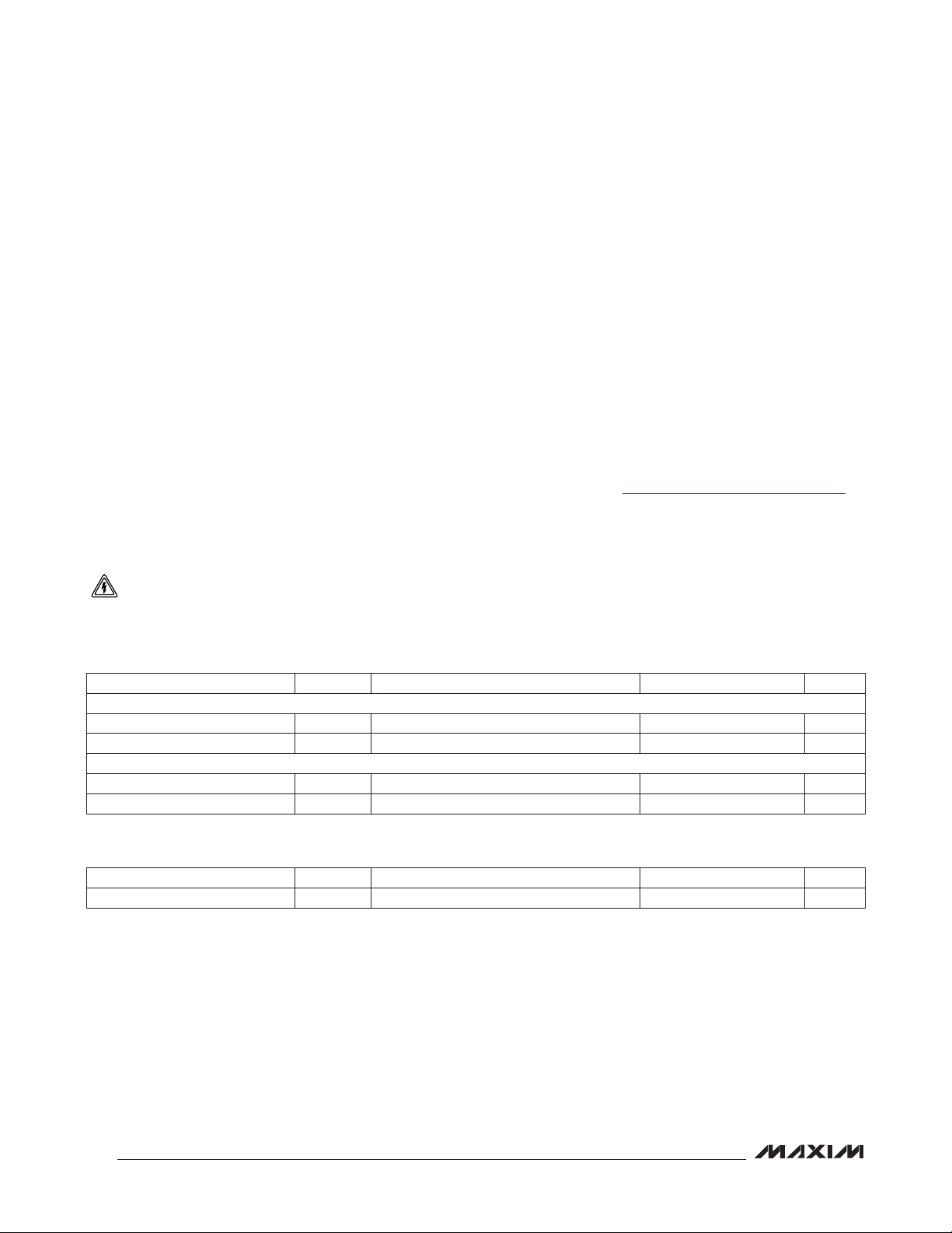
ABSOLUTE MAXIMUM RATINGS
VCC to GND ..........................................................-0.3V to +5.5V
CTRL to GND (with V
All Other Pins to GND .............................. -0.3V to (V
RF Input ......................................................................... +20dBm
Current into CTRL Pin (V
Maximum Junction Temperature .....................................+150°C
Operating Temperature Range .......................... -40°C to +85°C
Note 1: TC is the temperature on the exposed pad of the package. TA is the ambient temperature of the device and PCB.
MAX19790
Note 2: Based on junction temperature TJ = TC + (θJC x VCC x ICC). This formula can be used when the temperature of the exposed
pad is known while the device is soldered down to a PCB. See the Applications Information section for details. The junction
temperature must not exceed +150°C.
Note 3: Junction temperature T
known. The junction temperature must not exceed +150°C.
Note 4: Package thermal resistances were obtained using the method described in JEDEC specification JESD51-7, using a four-
layer board. For detailed information on package thermal considerations, refer to www.maxim-ic.com/thermal-tutorial.
Stresses beyond those listed under “Absolute Maximum Ratings” may cause permanent damage to the device. These are stress ratings only, and functional
operation of the device at these or any other conditions beyond those indicated in the operational sections of the specifications is not implied. Exposure to absolute
maximum rating conditions for extended periods may affect device reliability.
CAUTION! ESD SENSITIVE DEVICE
= +5.0V applied) ............ 0V to +4.75V
CC
grounded) .............................40mA
CC
= TA + (θJA x VCC x ICC). This formula can be used when the ambient temperature of the PCB is
J
+ 0.3V)
CC
Storage Temperature Range ........................….-65°C to +150°C
Continuous Power Dissipation (T
θ
(Notes 2, 4) ............................................................ +10°C/W
JC
θ
(Notes 3, 4) ............................................................ +35°C/W
JA
Lead Temperature (soldering, 10s) ................................+300°C
Soldering Temperature (reflow) ......................................+260°C
= +85°C) (Note 1) .......2.1W
C
DC ELECTRICAL CHARACTERISTICS
(VCC = +4.75V to +5.25V, V
-40°C to +85°C, unless otherwise noted. Typical values are at V
PARAMETER SYMBOL CONDITIONS MIN TYP MAX UNITS
SUPPLY
Supply Voltage V
Supply Current I
CONTROL INPUT
Control Voltage Range V
Control Input Resistance R
= +1.0V to +4.0V, no RF signals applied, all input and output ports terminated with 50I, TC =
CTRL
= +5.0V, V
CC
CC
CC
CTRL
CTRL
(Note 5) 1.0 4.0 V
RECOMMENDED AC OPERATING CONDITIONS
PARAMETER SYMBOL CONDITIONS MIN TYP MAX UNITS
RF Frequency Range f
RF
(Note 6) 250 4000 MHz
= +1.0V, TC = +25°C, unless otherwise noted.)
CTRL
4.75 5.0 5.25 V
7.3 9.5 mA
50
kI
2
Page 3
250MHz to 4000MHz Dual,
Analog Voltage Variable Attenuator
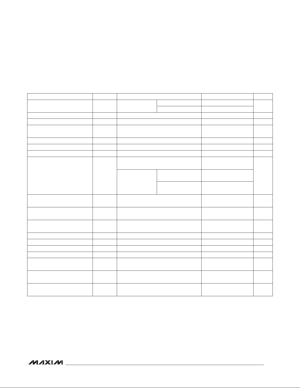
AC ELECTRICAL CHARACTERISTICS
(MAX19790 Evaluation Kit, line and connector losses included, two attenuators in cascade, VCC = 4.75V to 5.25V, RF ports are
driven from 50I sources, input P
for T
= +25°C, VCC = +5.0V, input PRF = -10dBm, fRF = 1500MHz, V
C
PARAMETER SYMBOL CONDITIONS MIN TYP MAX UNITS
Insertion Loss IL T
Loss Variation Over Temperature T
Input P
1dB
Input Second-Order Intercept
Point
Input Third-Order Intercept Point IIP3 f
Second Harmonic 2f
Third Harmonic 3f
Attenuation-Control Range A
Average Attenuation-Control
Slope
Maximum Attenuation-Control
Slope
Attenuation Flatness Over
125MHz Bandwidth (Note 8)
Switching Time From 15dB to 0dB attenuation (Note 9) 500 ns
Input Return Loss All gain settings 25 dB
Output Return Loss All gain settings 21 dB
Group Delay Input/output 50I lines deembedded 190 ps
Group-Delay Flatness Over
125MHz Bandwidth
Group-Delay Change vs.
Attenuation Control
Insertion Phase Change vs.
Attenuation Control
Note 5: Operating outside this range for extended periods may affect device reliability. Limit pin input current to 40mA when VCC
is not present (see Table 1 for R4 value).
Note 6: Operation outside this range is possible, but with degraded performance of some parameters. See the Typical Operating
Characteristics.
Note 7: f1 = 1500MHz, f2 = 1501MHz, -10dBm/tone at attenuator input.
Note 8: Guaranteed by design and characterization.
Note 9: Switching time is measured from 50% of the control signal to when the RF output settles to Q1dB.
= -10dBm, fRF = 950MHz to 2150MHz, V
RF
= +25NC
C
= -40NC to +85NC 0.6 dB
C
IP
1dB
f
+ f
IIP2
RF1
(Note 7)
RF1
IN
IN
One attenuator, V
to +4.0V, T
Two attenuators,
R
V
CTRL
to +4.0V,
T
= +25NC
C
V
CTRL
V
CTRL
Peak-to-peak for V
T
= +25NC
C
Peak-to-peak 10 ps
V
CTRL
V
CTRL
term, f
RF2
- f
RF2
= +1.0V
= +1.0V to +3.5V 20.0 dB/V
= +1.0V to +3.5V 30.4 dB/V
= +1.0V to +4.0V -175 ps
= +1.0V to +4.0V 82 Degrees
RF1
= 1MHz (Note 7) 36.3 dBm
CTRL
= +25NC
C
CTRL
= +1.0V, TC = -40°C to +85°C. Typical values are
CTRL
= +1.0V, unless otherwise noted.)
CTRL
950MHz to 1500MHz 4.4 6.3
950MHz to 2150MHz 4.4 7.0
23.1 dBm
- f
= 1MHz
RF2
= +1.0V
950MHz to 1500MHz 36 44.7
950MHz to 2150MHz 33 44.7
= +1.0V to +3.1V,
69.6 dBm
72 dBc
77 dBc
22
0.13 0.89 dB
dB
dB
MAX19790
3
Page 4
250MHz to 4000MHz Dual,
Analog Voltage Variable Attenuator
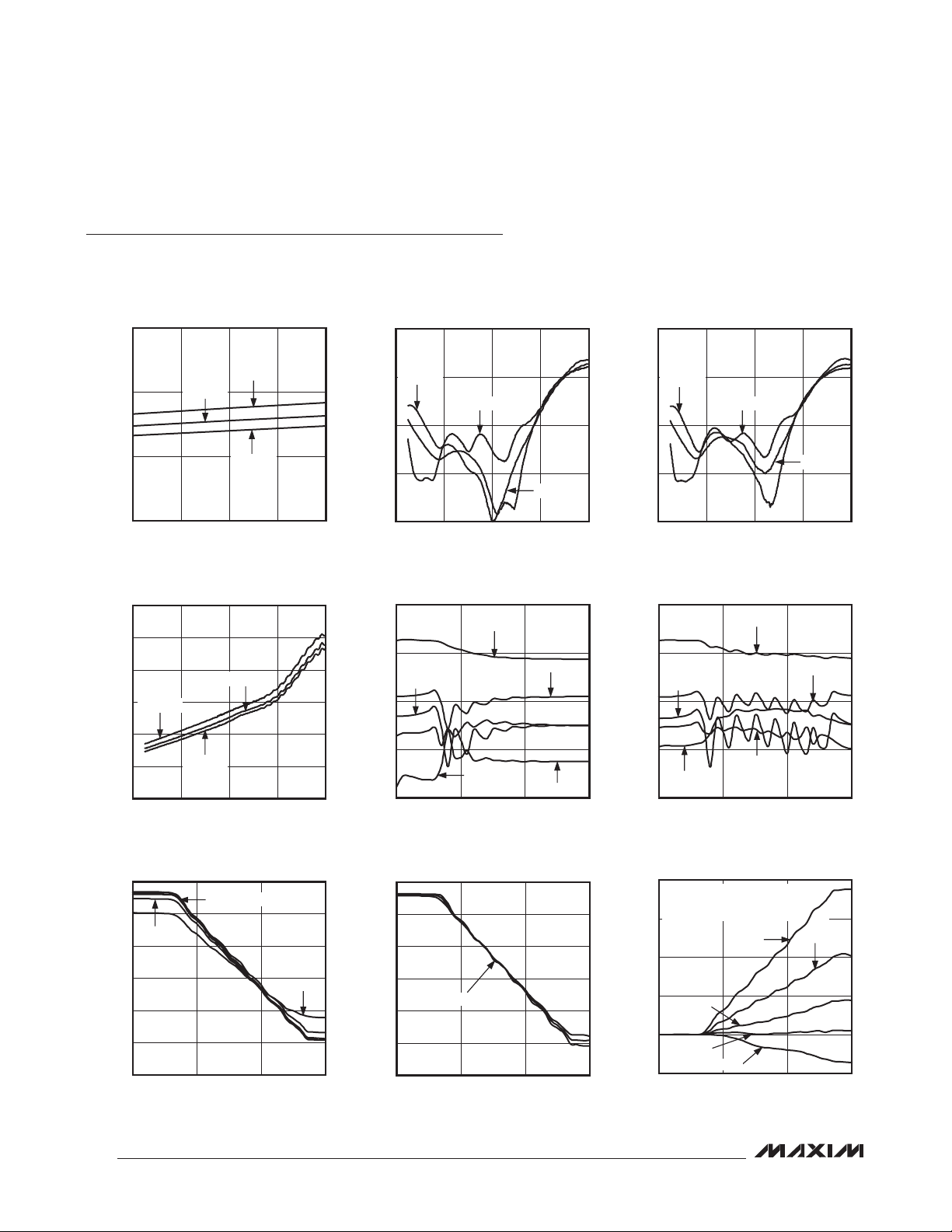
Typical Operating Characteristics
(MAX19790 Evaluation Kit, two attenuators in cascade, VCC = +5.0V, PRF = -10dBm, TC = +25NC, V
= +1.0V, unless otherwise noted.)
CTRL
8.0
MAX19790
7.5
7.0
SUPPLY CURRENT (mA)
6.5
4.750 5.250
TC = +25°C
VCC (V)
INSERTION LOSS vs. RF FREQUENCY
12
10
SUPPLY CURRENT vs. V
8
6
TC = +85°C
4
INSERTION LOSS (dB)
2
0
0 4000
TC = +25°C
TC = -40°C
RF FREQUENCY (MHz)
TC = +85°C
TC = -40°C
CC
MAX19790 toc01
5.1255.0004.875
MAX19790 toc04
300020001000
INPUT MATCH vs. RF FREQUENCY
0
-10
TC = +85°C
TC = -40°C
-20
S11 (dB)
-30
-40
0 4000
RF FREQUENCY (MHz)
INPUT MATCH vs. V
0
4000MHz
-10
500MHz
-20
S11 (dB)
-30
2150MHz
-40
1 4
V
(V)
CTRL
MAX19790 toc02
TC = +25°C
300020001000
CTRL
MAX19790 toc05
250MHz
950MHz
32
OUTPUT MATCH vs. RF FREQUENCY
0
-10
TC = +85°C
TC = -40°C
-20
S22 (dB)
-30
-40
0 4000
RF FREQUENCY (MHz)
OUTPUT MATCH vs. V
0
-10
500MHz
-20
S22 (dB)
-30
2150MHz
-40
1 4
4000MHz
950MHz
V
CTRL
32
(V)
MAX19790 toc03
TC = +25°C
300020001000
CTRL
MAX19790 toc06
250MHz
0
-10
2150MHz
-20
-30
S21 (dB)
-40
-50
-60
1 4
250MHz, 500MHz, 950MHz
V
CTRL
4
ATTENUATION vs. V
(V)
32
CTRL
4000MHz
MAX19790 toc07
0
ATTENUATION vs. V
-10
-20
-30
S21 (dB)
TC = -40°C, +25°C, +85°C
-40
-50
-60
1 4
V
(V)
CTRL
32
CTRL
f
RF
= 950MHz
S21 PHASE CHANGE vs. V
200
REFERENCED TO INSERTION-LOSS STATE.
POSITIVE PHASE = ELECTRICALLY
SHORTER.
150
MAX19790 toc08
100
50
950MHz
S21 PHASE CHANGE (DEGREES)
0
500MHz
-50
1 4
4000MHz
250MHz
V
CTRL
CTRL
MAX19790 toc09
2150MHz
32
(V)
Page 5
250MHz to 4000MHz Dual,
Analog Voltage Variable Attenuator
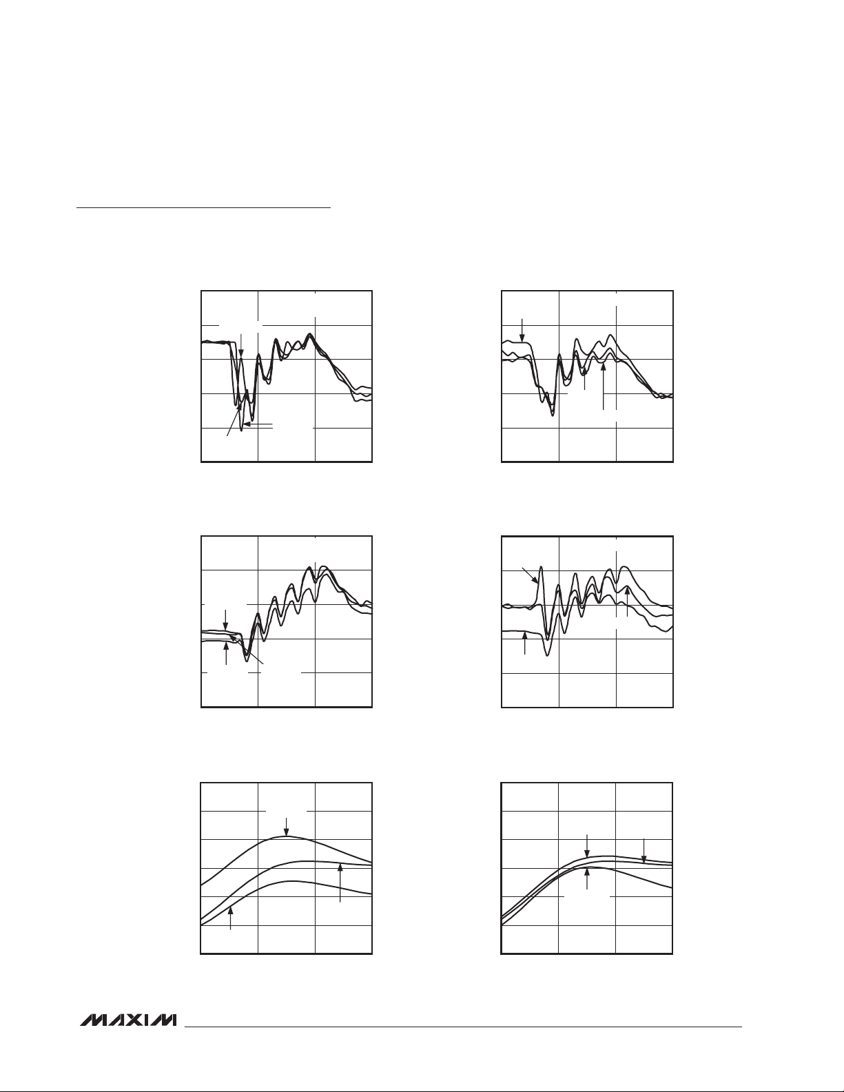
Typical Operating Characteristics (continued)
(MAX19790 Evaluation Kit, two attenuators in cascade, VCC = +5.0V, PRF = -10dBm, TC = +25NC, V
= +1.0V, unless otherwise noted.)
CTRL
MAX19790
45
P
TC = -40°C
V
(V)
CTRL
IN
40
TC = +85°C
35
30
INPUT IP3 (dBm)
25
TC = +25°C
20
1 4
INPUT IP2 vs. V
90
P
INPUT IP3 vs. V
80
TC = +25°C
70
60
INPUT IP2 (dBm)
TC = -40°C
50
TC = +85°C
IN
CTRL
fRF = 950MHz
= -10dBm/TONE
32
CTRL
fRF = 950MHz
= -10dBm/TONE
MAX19790 toc10
MAX19790 toc12
45
950MHz
40
35
30
INPUT IP3 (dBm)
25
20
1 4
1500MHz
2150MHz
V
CTRL
(V)
PIN = -10dBm/TONE
INPUT IP2 vs. V
INPUT IP3 vs. V
90
2150MHz
80
70
60
INPUT IP2 (dBm)
950MHz
50
PIN = -10dBm/TONE
CTRL
MAX19790 toc11
32
CTRL
MAX19790 toc13
1500MHz
40
1 4
V
INPUT P
26
25
24
(dBm)
1dB
23
INPUT P
22
21
TC = +85°C
20
950 2150
vs. RF FREQUENCY
1dB
TC = -40°C
RF FREQUENCY (MHz)
CTRL
32
(V)
17501350
TC = +25°C
MAX19790 toc14
40
1 4
V
INPUT P
26
25
24
(dBm)
1dB
23
INPUT P
22
21
20
950 2150
vs. RF FREQUENCY
1dB
VCC = 5.25V
VCC = 4.75V
RF FREQUENCY (MHz)
CTRL
32
(V)
17501350
MAX19790 toc15
VCC = 5.0V
5
Page 6

250MHz to 4000MHz Dual,
Analog Voltage Variable Attenuator
Typical Operating Characteristics (continued)
(MAX19790 Evaluation Kit, one attenuator connected, VCC = +5.0V, PRF = -10dBm, TC = +25NC, V
= +1.0V, unless otherwise noted.)
CTRL
8.0
MAX19790
7.5
7.0
SUPPLY CURRENT (mA)
6.5
4.750 5.250
TC = +25°C
VCC (V)
INSERTION LOSS vs. RF FREQUENCY
8
6
4
TC = +85°C
INSERTION LOSS (dB)
2
0
0 4000
RF FREQUENCY (MHz)
SUPPLY CURRENT vs. V
TC = +85°C
TC = -40°C
TC = +25°C
TC = -40°C
CC
MAX19790 toc16
5.1255.0004.875
MAX19790 toc19
300020001000
INPUT MATCH vs. RF FREQUENCY
0
TC = +85°C
-10
-20
S11 (dB)
-30
-40
-50
0 4000
TC = +25°C
TC = -40°C
RF FREQUENCY (MHz)
INPUT MATCH vs. V
0
-10
500MHz
-20
S11 (dB)
-30
-40
-50
1 4
4000MHz
250MHz
V
CTRL
32
(V)
MAX19790 toc17
300020001000
CTRL
MAX19790 toc20
2150MHz
950MHz
OUTPUT MATCH vs. RF FREQUENCY
0
-10
TC = +85°C
-20
S22 (dB)
-30
-40
-50
0 4000
TC = -40°C
TC = +25°C
RF FREQUENCY (MHz)
OUTPUT MATCH vs. V
0
-10
500MHz
-20
S22 (dB)
-30
-40
-50
1 4
2150MHz
4000MHz
950MHz
V
CTRL
250MHz
32
(V)
MAX19790 toc18
300020001000
CTRL
MAX19790 toc21
0
250MHz, 500MHz, 950MHz
-5
-10
2150MHz
-15
S21 (dB)
-20
-25
-30
1 4
4000MHz
V
CTRL
6
ATTENUATION vs. V
(V)
32
CTRL
MAX19790 toc22
0
ATTENUATION vs. V
-5
-10
-15
S21 (dB)
TC = -40°C, +25°C, +85°C
-20
-25
-30
1 4
V
(V)
CTRL
CTRL
fRF = 950MHz
32
S21 PHASE CHANGE vs. V
100
75
MAX19790 toc23
50
25
0
S21 PHASE CHANGE (DEGREES)
-25
REFERENCED TO INSERTION-LOSS STATE.
POSITIVE PHASE = ELECTRICALLY SHORTER.
-50
1 4
950MHz
4000MHz
500MHz
V
CTRL
CTRL
MAX19790 toc24
2150MHz
250MHz
32
(V)
Page 7

250MHz to 4000MHz Dual,
Analog Voltage Variable Attenuator
Typical Operating Characteristics (continued)
(MAX19790 Evaluation Kit, one attenuator connected, VCC = +5.0V, PRF = -10dBm, TC = +25NC, V
= +1.0V, unless otherwise noted.)
CTRL
MAX19790
45
P
TC = +25°C
TC = -40°C
V
(V)
CTRL
IN
40
35
30
INPUT IP3 (dBm)
25
TC = +85°C
20
1 4
INPUT IP2 vs. V
100
P
INPUT IP3 vs. V
90
80
= +25°C
T
C
70
INPUT IP2 (dBm)
60
TC = -40°C
50
1 4
TC = +85°C
V
CTRL
IN
(V)
CTRL
fRF = 950MHz
= -10dBm/TONE
32
CTRL
fRF = 950MHz
= -10dBm/TONE
32
MAX19790 toc25
MAX19790 toc27
45
1500MHz
40
35
30
INPUT IP3 (dBm)
25
20
1 4
2150MHz
V
CTRL
(V)
PIN = -10dBm/TONE
INPUT IP2 vs. V
INPUT IP3 vs. V
100
90
80
70
INPUT IP2 (dBm)
60
50
1 4
1500MHz
950MHz
V
(V)
CTRL
PIN = -10dBm/TONE
CTRL
MAX19790 toc26
950MHz
32
CTRL
MAX19790 toc28
2150MHz
32
INPUT P
26
25
24
(dBm)
1dB
23
INPUT P
22
21
TC = +25°C
20
950 2150
vs. RF FREQUENCY
1dB
TC = -40°C
17501350
RF FREQUENCY (MHz)
TC = +85°C
MAX19790 toc29
INPUT P
26
25
24
(dBm)
1dB
23
INPUT P
22
21
20
950 2150
vs. RF FREQUENCY
1dB
VCC = 5.25V
RF FREQUENCY (MHz)
VCC = 4.75V
17501350
VCC = 5.0V
MAX19790 toc30
7
Page 8

250MHz to 4000MHz Dual,
Analog Voltage Variable Attenuator
Pin Configuration/Functional Diagram
TOP VIEW
GND
GND
GND
GND
GND
GND
GND
GND
GND
192021222324252627
MAX19790
GND
OUT_B
GND
GND
V
GND
GND
IN_B
GND
28
29
30
31
32
CC
33
34
35
36
+
1 2 3 4 5 6 7 8 9
GND
ATTEN_B
GND
OUT_A
MAX19790
ATTENUATION-
CONTROL
CIRCUITRY
CC
V
GND
ATTEN_A
GND
GND
IN_A
*EP
GND
18
GND
17
GND
16
GND
15
GND
14
GND
13
V
CC
12
GND
CTRL
11
10
GND
THIN QFN
*EXPOSED PAD.
Pin Description
PIN NAME FUNCTION
1, 3, 4, 6, 7, 9, 10,
12, 14–28, 30, 31,
33, 34, 36
2 OUT_A
5, 13, 32 V
8 IN_A
11 CTRL
29 OUT_B
35 IN_B
— EP
GND Ground. Connect to the board’s ground plane using low-inductance layout techniques.
Attenuator A Output. Internally matched to 50I over the operating frequency band. This pin,
if used, requires a DC block. If this attenuator is not used, the pin can be left unconnected.
CC
Power Supply. Bypass to GND with capacitors and resistors as shown in the Typical
Application Circuit.
Attenuator A Input. Internally matched to 50I over the operating frequency band. This pin,
if used, requires a DC block. If this attenuator is not used, the pin can be left unconnected.
Analog Attenuator Control Input. V
must be present unless using a current-limiting resis-
CC
tor, as noted in the Applications Information section. Limit voltages applied to this pin to a
+1.0V to +4.0V range with V
present to ensure device reliability.
CC
Attenuator B Output. Internally matched to 50I over the operating frequency band. This pin,
if used, requires a DC block. If this attenuator is not used, the pin can be left unconnected.
Attenuator B Input. Internally matched to 50I over the operating frequency band. This pin,
if used, requires a DC block. If this attenuator is not used, the pin can be left unconnected.
Exposed Pad. Internally connected to GND. Solder evenly to the board’s ground plane for
proper operation.
8
Page 9

250MHz to 4000MHz Dual,
Analog Voltage Variable Attenuator
Detailed Description
The MAX19790 is a dual, general-purpose analog voltage variable attenuator (VVA) designed to interface
with 50I systems operating in the 250MHz to 4000MHz
frequency range. Each attenuator includes a control
circuit that provides 22dB of attenuation range with a
linear control slope of 10dB/V. Both attenuators share a
common analog control and can be cascaded together
to yield 44dB of total dynamic range, with a combined
linear control slope of 20dB/V.
Applications Information
Analog Attenuation Control
A single input voltage at the CTRL pin adjusts the attenuation of the device. Up to 22dB of attenuation-control
range is provided per attenuator. At the insertion-loss
setting, the attenuator’s loss is approximately 2.4dB.
If a larger attenuation-control range is desired, the
second on-chip attenuator can be connected in series to
provide an additional 22dB of gain-control range.
Note that the CTRL pin simultaneously adjusts both
on-chip attenuators. The CTRL input voltage drives a
high-impedance load (> 50kI). It is suggested that a
current-limiting resistor be included in series with this
connection, to limit the input current to less than 40mA,
should the control voltage be applied when V
CC
is not
present. A series resistor of greater than 200I provides
complete protection for +5.0V control voltage ranges.
Note: To ensure the reliability of the device, limit CTRL
input voltages to a +1.0V to +4.0V range when V
CC
is
present.
Layout Considerations
A properly designed PCB is an essential part of any
RF/microwave circuit. Keep RF signal lines as short as
possible to reduce losses, radiation, and inductance.
For best performance, route the ground-pin traces
directly to the exposed pad underneath the package.
This pad MUST be connected to the ground plane of
the board by using multiple vias under the device to
provide the best RF and thermal conduction path. Solder
the exposed pad on the bottom of the device package
to a PCB.
Power-Supply Bypassing
Proper voltage-supply bypassing is essential for highfrequency circuit stability. Bypass each V
pin with
CC
capacitors placed as close as possible to the device.
Place the smallest capacitor closest to the device. See
the Typical Application Circuit and Table 1 for details.
MAX19790
Table 1. Typical Application Circuit Component Values
DESIGNATION QTY DESCRIPTION
220pF Q5%, 50V C0G ceramic
C1, C3, C5 3
C2, C4 2
C6 1
C7 1
C8* 0
*C8 can be used to provide additional filtering. Depending on the external driver used on the CTRL line, this capacitance could
slow down the response time.
capacitors (0402)
Murata GRM1555C1H221J
0.01FF Q10%, 25V X7R ceramic
capacitors (0402)
Murata GRM155R71E103K
1000pF Q5%, 50V C0G ceramic
capacitor (0402)
Murata GRM1555C1H102J
0.1FF Q10%, 16V X7R ceramic
capacitor (0603)
Murata GRM188R71C104K
Not installed, ceramic capacitor
(0603)
DESIGNATION QTY DESCRIPTION
22pF Q5%, 50V C0G ceramic
C9 1
R1, R2 2
R3, R4 2
U1 1
capacitor (0402)
Murata GRM1555C1H220J
10I Q5% resistors (0402)
Any
0I resistors (0402)
Note: In cases where V
applied before or removed after
V
, use R4 = 200I.
CC
Analog attenuator IC
Maxim MAX19790ETX+
Note: U1 has an exposed pad
conductor, which requires it to be
solder-attached to a grounded
pad on the PCB to ensure a
proper electrical/thermal design.
CTRL
is
9
Page 10

250MHz to 4000MHz Dual,
Analog Voltage Variable Attenuator
Exposed Pad RF and Thermal
Considerations
The exposed pad (EP) of the device’s 36-pin thin QFN
package provides a low thermal-resistance path to
the die. It is important that the PCB on which the IC is
The EP MUST be soldered to a ground plane on the
PCB, either directly or through an array of plated via
holes. Soldering the pad to ground is also critical
for efficient heat transfer. Use a solid ground plane
wherever possible.
mounted be designed to conduct heat from this contact.
In addition, provide the EP with a low-inductance RF
ground path for the device.
MAX19790
Typical Application Circuit
GND
GND
GND
GND
GND
GND
GND
GND
GND
EP
IN_A
192021222324252627
GND
GND
18
GND
17
GND
16
GND
15
GND
14
V
CC
13
GND
12
CTRL
11
GND
10
V
CC
CTRL
R3
C7
C6
C9
C8
R4
RFOUT
C5
C4
V
CC
R2
C3
GND
OUT_B
GND
GND
V
GND
GND
IN_B
GND
28
29
30
31
CC
32
33
34
35
36
ATTEN_B
2 3 4 5 6 7 8 9
1
GND
OUT_A
GND
MAX19790
CC
V
GND
R1
ATTENUATION-
CONTROL
CIRCUITRY
ATTEN_A
GND
GND
C1
10
V
RFB*
*SCHEMATIC SHOWS CONFIGURATION FOR TWO CASCADED ATTENUATORS. TO USE ATTENUATOR A ONLY MOVE C3
TO CONNECT OUT_A TO RFB. TO USE ATTENUATOR B ONLY MOVE C3 TO CONNECT RFB TO IN_B.
CC
C2
RFA
Page 11

250MHz to 4000MHz Dual,
Analog Voltage Variable Attenuator
Chip Information
PROCESS: BiCMOS
Package Information
For the latest package outline information and land patterns,
go to www.maxim-ic.com/packages. Note that a “+”, “#”, or
“-” in the package code indicates RoHS status only. Package
drawings may show a different suffix character, but the drawing
pertains to the package regardless of RoHS status.
PACKAGE TYPE PACKAGE CODE DOCUMENT NO.
36 Thin QFN-EP T3666+2
21-0141
MAX19790
Maxim cannot assume responsibility for use of any circuitry other than circuitry entirely embodied in a Maxim product. No circuit patent licenses are implied.
Maxim reserves the right to change the circuitry and specifications without notice at any time.
Maxim Integrated Products, 120 San Gabriel Drive, Sunnyvale, CA 94086 408-737-7600 11
©
2010 Maxim Integrated Products Maxim is a registered trademark of Maxim Integrated Products, Inc.
 Loading...