

19-0435; Rev 0; 9/95
EVALUATION KIT
AVAILABLE
Multirange, Single +5V, 12-Bit DAS
with 12-Bit Bus Interface
_______________General Description
The MAX196/MAX198 multirange, 12-bit data-acquisition systems (DAS) require only a single +5V supply for
operation, yet convert analog signals at their inputs up
to ±10V (MAX196) and ±4V (MAX198). These systems
provide six analog input channels that are independently software programmable for a variety of ranges:
±10V, ±5V, 0V to +10V, and 0V to +5V for the MAX196;
±V
, ±V
REF
/2, 0V to +V
REF
, and 0V to +V
REF
REF
/2 for
the MAX198. This range switching increases the effective dynamic range to 14 bits and provides the flexibility
to interface ±12V, ±15V, and 4mA to 20mA powered
sensors to a single +5V system. In addition, these converters are fault protected to ±16.5V; a fault condition
on any channel will not affect the conversion result of
the selected channel. Other features include a 5MHz
bandwidth track/hold, 100ksps throughput rate, software-selectable internal/external clock, internal/external
acquisition control, 12-bit parallel interface, and internal
4.096V or external reference.
Two programmable power-down modes (STBYPD,
FULLPD) provide low-current shutdown between conversions. In STBYPD mode, the reference buffer
remains active, eliminating start-up delays.
The MAX196/MAX198 employ a standard microprocessor (µP) interface. A three-state data I/O port is configured to operate with 16-bit data buses, and dataaccess and bus-release timing specifications are compatible with most popular µPs. All logic inputs and outputs are TTL/CMOS compatible.
These devices are available in 28-pin DIP, wide SO,
SSOP (55% smaller in area than wide SO), and ceramic
SB packages. For 8+4 bus interface, see the MAX197
and the MAX199 data sheets. An evaluation kit will be
available after December 1995 (MAX196EVKIT-DIP).
________________________Applications
Industrial-Control Systems
Robotics
Data-Acquisition Systems
Automatic Testing Systems
Medical Instruments
Telecommunications
Functional Diagram appears at end of data sheet.
____________________________Features
♦ 12-Bit Resolution, 1/2LSB Linearity
♦ Single +5V Supply Operation
♦ Software-Selectable Input Ranges:
±10V, ±5V, 0V to +10V, 0V to +5V (MAX196)
±V
, ±V
REF
(MAX198)
/2, 0V to +V
REF
, 0V to +V
REF
REF
/2
♦ Internal 4.096V or External Reference
♦ Fault-Protected Input Multiplexer
♦ 6 Analog Input Channels
♦ 6µs Conversion Time, 100ksps Sampling Rate
♦ Internal or External Acquisition Control
♦ Two Power-Down Modes
♦ Internal or External Clock
______________Ordering Information
PART
MAX196ACNI
MAX196BCNI
MAX196ACWI 0°C to +70°C
MAX196BCWI 0°C to +70°C 28 Wide SO
MAX196ACAI 0°C to +70°C 28 SSOP
MAX196BCAI 0°C to +70°C 28 SSOP
Ordering Information continued at end of data sheet.
TEMP. RANGE PIN-PACKAGE
0°C to +70°C
0°C to +70°C
28 Narrow Plastic DIP
28 Narrow Plastic DIP
28 Wide SO
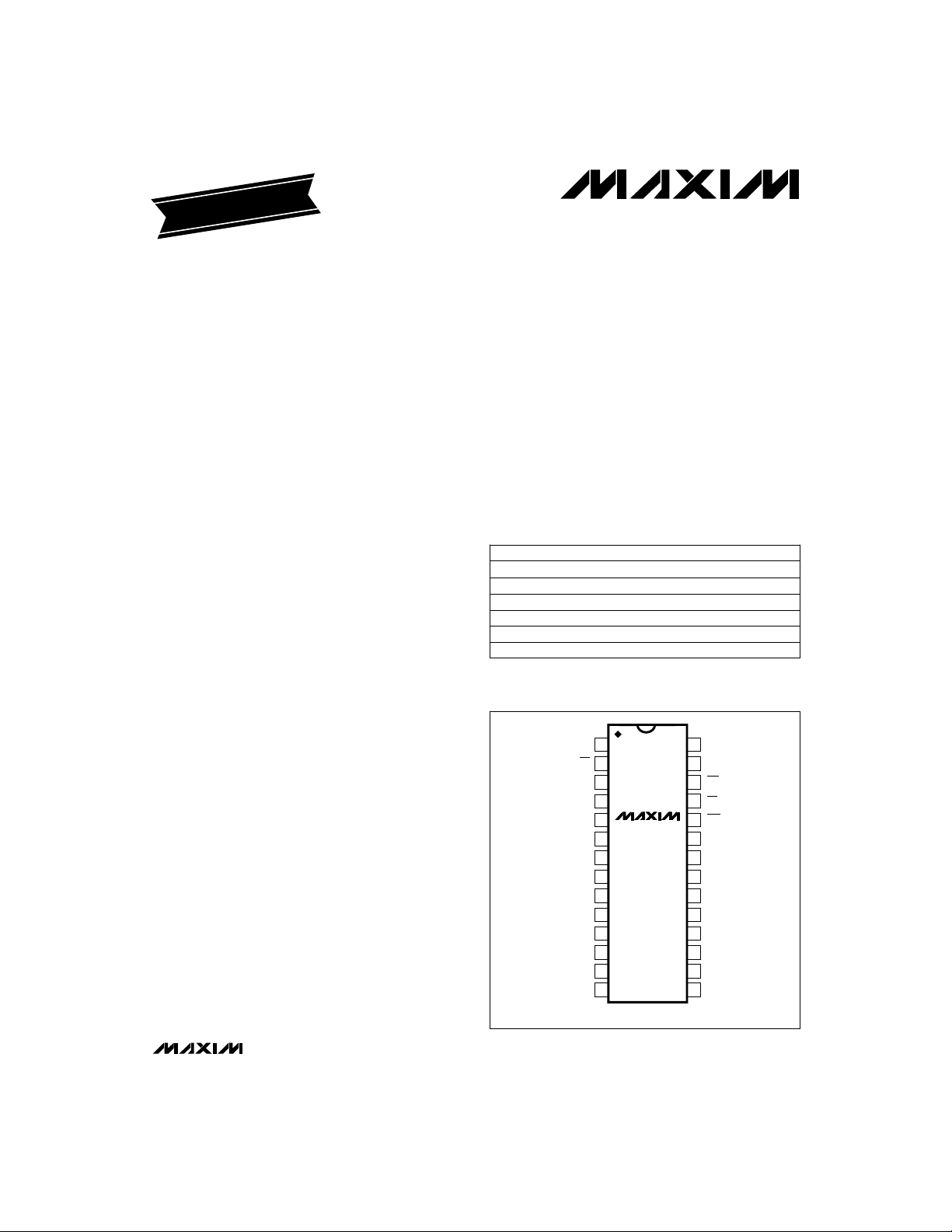
__________________Pin Configuration
TOP VIEW
CLK
1
CS
2
D11
3
D10
4
D9
5
D8
D7
D6
D5
D4
D3
D2
D1
D0
DIP/SO/SSOP/Ceramic SB
MAX196
6
MAX198
7
8
9
10
11
12
13
14
28
27
26
25
24
23
22
21
20
19
18
17
16
15
DGND
V
DD
WR
RD
INT
REF
REFADJ
CH5
CH4
CH3
CH2
CH1
CH0
AGND
MAX196/MAX198
________________________________________________________________
Maxim Integrated Products
Call toll free 1-800-722-8266 for free samples or literature.
1
Multirange, Single +5V, 12-Bit DAS
with 12-Bit Bus Interface
ABSOLUTE MAXIMUM RATINGS
VDDto AGND............................................................-0.3V to +7V
AGND to DGND.....................................................-0.3V to +0.3V
REF to AGND..............................................-0.3V to (V
REFADJ to AGND.......................................-0.3V to (V
Digital Inputs to DGND...............................-0.3V to (V
Digital Outputs to DGND............................-0.3V to (V
CH0–CH5 to AGND ..........................................................±16.5V
Continuous Power Dissipation (T
Narrow Plastic DIP (derate 14.29mW/°C above +70°C)....1143mW
Stresses beyond those listed under “Absolute Maximum Ratings” may cause permanent damage to the device. These are stress ratings only, and functional
operation of the device at these or any other conditions beyond those indicated in the operational sections of the specifications is not implied. Exposure to
absolute maximum rating conditions for extended periods may affect device reliability.
= +70°C)
A
DD
DD
DD
DD
+ 0.3V)
+ 0.3V)
+ 0.3V)
+ 0.3V)
ELECTRICAL CHARACTERISTICS
(VDD= 5V ±5%; unipolar/bipolar range; external reference mode, V
with 50% duty cycle; T
MAX196/MAX198
ACCURACY (Note 1)
Offset Error
Channel-to-Channel Offset
Error Matching
Gain Error
(Note 2)
Gain Temperature Coefficient
(Note 2)
DYNAMIC SPECIFICATIONS (10kHz sine-wave input, ±10Vp-p (MAX196) or ±4.096Vp-p (MAX198), f
= T
to T
A
MIN
; unless otherwise noted. Typical values are at TA= +25°C.)
MAX
MAX196A/MAX198A
INLIntegral Nonlinearity
MAX196B/MAX198B
Unipolar
Bipolar
Unipolar
Bipolar
Unipolar
Bipolar
Unipolar
Bipolar
SINADSignal-to-Noise + Distortion Ratio
MAX196A/MAX198A
MAX196B/MAX198B 69
Up to the 5th harmonic
MAX196A/MAX198A
MAX196B/MAX198B
MAX196A/MAX198A
MAX196B/MAX198B
MAX196A/MAX198A
MAX196B/MAX198B
MAX196A/MAX198A
MAX196B/MAX198B
Wide SO (derate 12.50mW/°C above +70°C)..............1000mW
SSOP (derate 9.52mW/°C above +70°C) ......................762mW
Narrow Ceramic SB (derate 20.00mW/°C above +70°C)..1600mW
Operating Temperature Ranges
MAX196_C_ I/MAX198_C_ I .................................0°C to +70°C
MAX196_E_ I/MAX198_E_ I...............................-40°C to +85°C
MAX196_MYI/MAX198_MYI.............................-55°C to +125°C
Storage Temperature Range.............................-65°C to +150°C
Lead Temperature (soldering, 10sec).............................+300°C
= 4.096V; 4.7µF at REF pin; external clock, f
REF
CONDITIONS
±1/2
±1
±3
±5
±5
±10
±0.1
±0.5
±7
±10
±7
±10
3
5
= 100ksps)
SAMPLE
70
CLK
= 2.0MHz
UNITSMIN TYP MAXSYMBOLPARAMETER
ppm/°C
Bits12Resolution
LSB
LSB±1DNLDifferential Nonlinearity
LSB
LSB
LSB
dB
dB-85 -78THDTotal Harmonic Distortion
dB80SFDRSpurious-Free Dynamic Range
50kHz, VIN= ±5V (MAX196) or ±4V (MAX198)
(Note 3)
External CLK mode/external acquisition control
External CLK mode/external acquisition control
Aperture Jitter
2 _______________________________________________________________________________________
Internal CLK mode/internal acquisition
control (Note 4)
10
dB-86Channel-to-Channel Crosstalk
ns15Aperture Delay
ps<50
ns
Multirange, Single +5V, 12-Bit DAS
with 12-Bit Bus Interface
ELECTRICAL CHARACTERISTICS (continued)
(VDD= 5V ±5%; unipolar/bipolar range; external reference mode, V
with 50% duty cycle; T
PARAMETER SYMBOL MIN TYP MAX UNITS
ANALOG INPUT
Track/Hold Acquisition Time 3 µs
Small-Signal Bandwidth
Input Voltage Range
(see Table 3)
Input Current
Input Resistance
Input Capacitance 40 pF
INTERNAL REFERENCE
REF Output Voltage V
REF Output Tempco
(Contact Maxim Applications for
guaranteed temperature drift
specifications)
Output Short-Circuit Current 30 mA
Load Regulation 10 mV0mA to 0.5mA output current (Note 6)
Capacitive Bypass at REF 4.7 µF
REFADJ Output Voltage 2.465 2.500 2.535 V
REFADJ Adjustment Range ±1.5 %With recommended circuit (Figure 1)
Buffer Voltage Gain 1.6384 V/V
= T
to T
A
MIN
; unless otherwise noted. Typical values are at TA= +25°C.)
MAX
CONDITIONS
f
= 2.0MHz
∆V
∆I
TC V
CLK
-3dB
rolloff
Unipolar
V
IN
Bipolar
Unipolar
I
IN
Bipolar
Unipolar
IN
IN
Bipolar
(Note 5)
TA= +25°C
REF
MAX196_C/MAX198_C
REF
±10V or ±V
±5V or ±V
0V to 10V or 0V to V
0V to 5V or 0V to V
MAX196
MAX198
MAX196
MAX198
MAX196
MAX198
MAX196
MAX198
= 4.096V; 4.7µF at REF pin; external clock, f
REF
range
REF
/2 range
REF
0V to 10V range
0V to 5V range
±10V range
±5V range
±V
REF
±V
REF
REF
/2 range
REF
range
/2 range
range
1.25
010
05
0V
0V
-10 10
-5 5
-V
REF
-V
/2 V
REF
-1200 720
-600 360
-1200 10
-600 10
4.076 4.096 4.116 V
5
2.5
2.5
REF
V
REF
720
360
0.1 10
21
16
15
30MAX196_E/MAX198_E
40MAX196_M/MAX198_M
CLK
REF
REF
= 2.0MHz
/2
/2
ppm/°C
MAX196/MAX198
MHz
V
µA
kΩ
_______________________________________________________________________________________ 3
Multirange, Single +5V, 12-Bit DAS
with 12-Bit Bus Interface
ELECTRICAL CHARACTERISTICS (continued)
(VDD= 5V ±5%; unipolar/bipolar range; external reference mode, V
with 50% duty cycle; T
REFERENCE INPUT (buffer disabled, reference input applied to REF pin)
Input Current
Input Resistance
REFADJ Threshold for
Buffer Disable
POWER REQUIREMENTS
MAX196/MAX198
Supply Voltage
Supply Current
Power-Supply Rejection Ratio
(Note 8)
TIMING
Internal Clock Frequency
External Clock Frequency Range MHz
Acquisition Time
Conversion Time
Throughput Rate
Bandgap Reference
Start-Up Time
Reference Buffer Settling
DIGITAL INPUTS (D7–D0, CLK, RD, WR, CS) (Note 11)
Input High Voltage V
Input Low Voltage V
Input Leakage Current I
Input Capacitance
= T
to T
A
MIN
; unless otherwise noted. Typical values are at TA= +25°C.)
MAX
Normal, or STANDBY
=
power-down mode
FULL power-down mode
= 100pF MHz1.25 1.56 2.00f
CLK
CLK
DD
DD
I
DD
PSRR
CLK
CLK
t
ACQI
t
ACQE
t
CONV
INH
INL
IN
C
IN
V
REF
4.18V
Normal, or STANDBY power-down mode kΩ10
FULL power-down mode 5 MΩ
Normal mode, bipolar ranges
Normal mode, unipolar ranges
STANDBY power-down mode
FULL power-down mode (Note 7)
External reference = 4.096V
Internal reference ±1/
C
CLK
Internal acquisition
External acquisition (Note 9)
After FULLPD or STBYPD
External CLK
Internal CLK, C
External CLK
Internal CLK, C
Power-up (Note 10) µs200
To 0.1mV REF bypass
capacitor fully discharged
= 4.096V; 4.7µF at REF pin; external clock, f
REF
CONDITIONS
610
700 850
60 120
±0.1 ±1/
2
0.1 2.0f
External CLK
Internal CLK
= 100pF 6.0 7.7 10.0
= 100pF 62
C
= 4.7µF
REF
C
= 33µF
REF
3.0
3.0 5.0
3.0
5
6.0
8
60
2.4 V
= 2.0MHz
CLK
UNITSMIN TYP MAXSYMBOLPARAMETER
400
1
18
2
100
0.8 V
±10 µAVIN= 0V or V
15 pF(Note 5)
V2.4 4.18Input Voltage Range
µA
VVDD- 50mV
V4.75 5.25V
mA
µA
LSB
µs
µs
ksps
ms
4 _______________________________________________________________________________________
Multirange, Single +5V, 12-Bit DAS
with 12-Bit Bus Interface
ELECTRICAL CHARACTERISTICS (continued)
(VDD= 5V ±5%; unipolar/bipolar range; external reference mode, V
with 50% duty cycle; T
PARAMETER SYMBOL MIN TYP MAX UNITSCONDITIONS
DIGITAL OUTPUTS (D11–D0, INT)
Output Low Voltage V
Output High Voltage V
Three-State Output Capacitance C
= T
to T
A
MIN
; unless otherwise noted. Typical values are at TA= +25°C.)
MAX
OL
OH
OUT
SINK
SOURCE
= 4.096V; 4.7µF at REF pin; external clock, f
REF
= 1.6mA
= 1mA
VDD- 1 VVDD= 4.75V, I
CLK
0.4 VVDD= 4.75V, I
15 pF(Note 5)
= 2.0MHz
TIMING CHARACTERISTICS
(VDD= 5V ±5%; unipolar/bipolar range; external reference mode, V
with 50% duty cycle; T
PARAMETER SYMBOL MIN TYP MAX UNITS
CS Pulse Width t
WR Pulse Width t
CS to WR Setup Time
CS to WR Hold Time t
CS to RD Setup Time
CS to RD Hold Time t
CLK to WR Setup Time
CLK to WR Hold Time t
Data Valid to WR Setup
Data Valid to WR Hold t
RD Low to Output Data Valid
RD High to Output Disable
RD Low to INT High Delay
Note 1: Accuracy specifications tested at VDD= 5.0V. Performance at power-supply tolerance limits guaranteed by Power-Supply
Note 2: External reference: V
Note 3: Ground “on” channel; sine wave applied to all “off” channels.
Note 4: Maximum full-power input frequency for 1LSB error with 10ns jitter = 3kHz.
Note 5: Guaranteed by design. Not tested.
Note 6: Use static loads only.
Note 7: Tested using internal reference.
Note 8: PSRR measured at full-scale.
Note 9: External acquisition timing: starts at data valid at ACQMOD = low control byte; ends at rising edge of WR
Note 10: Not subject to production testing. Provided for design guidance only.
Note 11: All input control signals specified with t
Note 12: t
Note 13: t
Rejection test. Tested for the ±10V (MAX196) and ±4.096V (MAX198) input ranges.
= high control byte.
is measured with the load circuits of Figure 2 and defined as the time required for an output to cross 0.8V or 2.4V.
DO
is defined as the time required for the data lines to change by 0.5V.
TR
= T
to T
A
MIN
; unless otherwise noted.)
MAX
CONDITIONS
CS
WR
t
CSWS
CSWH
t
CSRS
CSRH
t
CWS
CWH
t
DS
DH
t
DO
t
TR
t
INT1
= 4.096V, offset error nulled, ideal last code transition = FS - 3/2LSB.
REF
= tF= 5ns from a voltage level of 0.8V to 2.4V.
R
= 4.096V; 4.7µF at REF pin; external clock, f
REF
80 ns
80 ns
0 ns
0 ns
0 ns
0 ns
60 ns
0 ns
= 2.0MHz
CLK
100 ns
50 ns
120 nsFigure 2, CL= 100pF (Note 12)
70 ns(Note 13)
120 ns
with ACQMOD
MAX196/MAX198
_______________________________________________________________________________________ 5

Multirange, Single +5V, 12-Bit DAS
with 12-Bit Bus Interface
__________________________________________Typical Operating Characteristics
(TA = +25°C, unless otherwise noted.)
INTEGRAL NONLINEARITY
0.250
0.200
0.150
0.100
0.050
0
-0.050
INTEGRAL NONLINEARITY (LSB)
-0.100
MAX196/MAX198
-0.150
vs. DIGITAL CODE
0 1000 3000
2000 4000
DIGITAL CODE
REFERENCE OUTPUT VOLTAGE (V
4.100
4.095
(V)
4.090
REF
V
4.085
4.080
-55
-35 45
vs. TEMPERATURE
+2.5V
INTERNAL
REFERENCE
REFADJ
525 65
-15
TEMPERATURE (°C)
MAX196/8-1
A
V
= 1.6384
0
-20
-40
-60
AMPLITUDE (dB)
-80
-100
-120
)
REF
REF
105 125
85
FFT PLOT
05025
FREQUENCY (kHz)
MAX196/8-4
f
TONE
f
SAMPLE
= 10kHz
= 100kHz
12.0
MAX196/8-2
11.5
11.0
10.5
EFFECTIVE NUMBER OF BITS
10.0
POWER-SUPPLY REJECTION RATIO
0.4
vs. TEMPERATURE
120Hz
0.2
0
100Hz
-0.2
PSRR (LSB)
-0.4
-0.6
-70 -50
-30 -10 10 30 70 90
TEMPERATURE (°C)
EFFECTIVE NUMBER OF BITS
vs. INPUT FREQUENCY
f
= 100kHz
SAMPLE
1 10 100
INPUT FREQUENCY (kHz)
= 5V ±0.25V
V
DD
50
110
130
MAX196/8-5
MAX196/8-3
OFFSET-ERROR MATCHING vs. TEMPERATURE
CHANNEL-TO-CHANNEL
OFFSET-ERROR MATCHING (LSB)
CHANNEL-TO-CHANNEL
0.20
0.18
0.16
0.14
0.12
0.10
-70 -50 50 110
-30 -10 10 30 70 90
TEMPERATURE (°C)
130
MAX196/8-6
CHANNEL-TO-CHANNEL
CHANNEL-TO-CHANNEL
GAIN-ERROR MATCHING vs. TEMPERATURE
0.33
0.32
0.31
0.30
0.29
GAIN-ERROR MATCHING (LSB)
0.28
0.27
-70 -50 50 110
-30 -10 10 30 70 90
TEMPERATURE (°C)
6 _______________________________________________________________________________________
MAX196/8-7
130

Multirange, Single +5V, 12-Bit DAS
with 12-Bit Bus Interface
______________________________________________________________Pin Description
PIN
Clock Input. In external clock mode, drive CLK with a TTL/CMOS-compatible clock. In internal clock mode,
CLK1
REFADJ22
REF23
WR26
27
+5V
100k
24k
Figure 1. Reference-Adjust Circuit
D
OUT
3k
a) High-Z to V
Figure 2. Load Circuits for Enable Time
place a capacitor (C
with C
Chip Select, active lowCS2
Three-State Digital I/O, D11 = MSBD11–D03–14
Analog GroundAGND15
Analog Input ChannelsCH0–CH516–21
Bandgap Voltage-Reference Output/External Adjust Pin. Bypass with a 0.01µF capacitor to AGND. Connect
to VDDwhen using an external reference at the REF pin.
Reference Buffer Output/ADC Reference Input. In internal reference mode, the reference buffer provides a
4.096V nominal output, externally adjustable at REFADJ. In external reference mode, disable the internal
buffer by pulling REFADJ to VDD.
INT goes low when conversion is complete and output data is ready.INT24
If CS is low, a falling edge on RD will enable a read operation on the data bus.RD25
In the internal acquisition mode, when CSis low, a rising edge on WR latches in configuration data and starts an
acquisition plus a conversion cycle. In the external acquisition mode, when CSis low, the first rising edge on WR
starts an acquisition, and a second rising edge on WRends acquisition and starts a conversion cycle.
+5V Supply. Bypass with 0.1µF capacitor to AGND.V
DD
Digital GroundDGND28
510k
0.01µF
C
and VOL to V
OH
LOAD
OH
= 100pF.
CLK
REFADJ
D
b) High-Z to VOL and VOH to V
) from this pin to ground to set the internal clock frequency; f
CLK
MAX196
MAX198
+5V
3k
OUT
C
LOAD
OL
FUNCTIONNAME
= 1.56MHz typical
CLK
_______________Detailed Description
The MAX196/MAX198 multirange, fault-tolerant ADCs
use successive approximation and internal input
track/hold (T/H) circuitry to convert an analog signal to
a 12-bit digital output. The 12-bit parallel-output format
provides easy interface to microprocessors (µPs).
Figure 3 shows the MAX196/MAX198 in the simplest
operational configuration.
In the internal acquisition control mode (control bit D5
set to 0), the T/H enters its tracking mode on WR’s rising edge, and enters its hold mode when the internally
timed (6 clock cycles) acquisition interval ends. In bipolar mode and unipolar mode (MAX196 only), a lowimpedance input source, which settles in less than
1.5µs, is required to maintain conversion accuracy at
the maximum conversion rate.
When the MAX198 is configured for unipolar mode, the
input does not need to be driven from a low-impedance
source. The acquisition time (tAZ) is a function of the
source output resistance (RS), the channel input resistance (RIN), and the T/H capacitance.
Converter Operation
Analog-Input Track/Hold
MAX196/MAX198
_______________________________________________________________________________________ 7

Multirange, Single +5V, 12-Bit DAS
with 12-Bit Bus Interface
Acquisition time is calculated as follows:
For 0V to V
For 0V to V
: tAZ= 9 x (RS+ RIN) x 16pF
REF
/2: tAZ= 9 x (RS+ RIN) x 32pF
REF
where RIN= 7kΩ and tAZis never less than 2µs (0V to
V
range) or 3µs (0V to V
REF
/2 range).
REF
In the external acquisition control mode (D5 = 1), the
T/H enters its tracking mode on the first WR rising edge
and enters its hold mode when it detects the second
WR rising edge with D5 = 0 (see
External Acquisition
section).
1
100pF
MAX196/MAX198
µP
CONTROL
INPUTS
µP DATA BUS
CLK
MAX196
25
MAX198
RD
26
WR
2
CS
3
D11
4
D10
5
D9
6
D8
7
D7
8
D6
9
D5
10
D4
11
D3
12
D2
13
D1
14
D0
Figure 3. Operational Diagram
S1
5.12k
R1
CH_
S1 = BIPOLAR/UNIPOLAR SWITCH
S2 = INPUT MUX SWITCH
S3, S4 = T/H SWITCH
S2
R2
R1 = 12.5kΩ (MAX196) OR 5.12kΩ (MAX198)
R2 = 8.67kΩ (MAX196) OR ∞ (MAX198)
Figure 4. Equivalent Input Circuit
DGND
V
REF
REFADJ
CH5
CH4
CH3
CH2
CH1
CH0
AGND
BIPOLAR
UNIPOLAR
OFF
ON
DD
INT
S3
TRACKHOLD
28
27
23
22
0.01µF 0.01µF
24
21
20
19
18
17
16
15
C
HOLD
4.7µF4.7µF
OUTPUT STATUS
ANALOG
INPUTS
VOLTAGE
REFERENCE
S4
T/H
OUT
The ADC’s input tracking circuitry has a 5MHz small-
Input Bandwidth
signal bandwidth. When using the internal acquisition
mode with an external clock frequency of 2MHz, a
100ksps throughput rate can be achieved. It is possible
to digitize high-speed transient events and measure
periodic signals with bandwidths exceeding the ADC’s
sampling rate by using undersampling techniques. To
avoid high-frequency signals being aliased into the frequency band of interest, anti-alias filtering is recommended (MAX274/MAX275 continuous-time filters).
Input Range and Protection
Figure 4 shows the equivalent input circuit. The fullscale input voltage depends on the voltage at the refer-
+5V
ence (V
allows input voltage ranges of ±10V, ±5V, 0V to +10V,
). The MAX196 uses a scaling factor, which
REF
or 0V to +5V with a 4.096V voltage reference (Table 1).
Program the desired range by setting the appropriate
control bits (D3, D4) in the control byte (Tables 2 and
3). The MAX198 does not use a scaling factor, so its
input voltage range directly corresponds with the reference voltage. It can be programmed for input voltages
of ±V
REF
, ±V
/2, 0V to V
REF
, or 0V to V
REF
REF
/2 (Table
3). When an external reference is applied at REFADJ,
the voltage at REF is given by V
(2.4V < V
REF
< 4.18V).
= 1.6384 x V
REF
REFADJ
The input channels are overvoltage protected to
±16.5V. This protection is active even if the device is in
power-down mode.
Even with VDD= 0V, the input resistive network provides
current-limiting that adequately protects the device.
Digital Interface
Input data (control byte) and output data are multiplexed on a three-state parallel interface. This parallel
I/O can easily be interfaced with a µP. CS, WR, and RD
control the write and read operations. CS is the standard chip-select signal, which enables a µP to address
the MAX196/MAX198 as an I/O port. When high, it disables the WR and RD inputs and forces the interface
into a high-Z state.
Table 1. Full Scale and Zero Scale
HOLDTRACK
(MAX196 only)
RANGE (V)
0 to +5 0 — V
0 to +10 0 — V
ZERO SCALE
(V) -FULL SCALE +FULL SCALE
±5 — -V
±10 — -V
x 1.2207 V
REF
x 2.4414 V
REF
REF
REF
REF
REF
x 1.2207
x 2.4414
x 1.2207
x 2.4414
8 _______________________________________________________________________________________

Multirange, Single +5V, 12-Bit DAS
with 12-Bit Bus Interface
Table 2. Control-Byte Format
D7 (MSB) D6 D5 D4 D3 D2 D1 D0 (LSB)
PD1 PD0 ACQMOD RNG BIP A2 A1 A0
BIT NAME DESCRIPTION
7, 6 PD1, PD0 These two bits select the clock and power-down modes (Table 4).
5 ACQMOD 0 = internally controlled acquisition (6 clock cycles), 1 = externally controlled acquisition
4 RNG Selects the full-scale voltage magnitude at the input (Table 3).
3 BIP Selects unipolar or bipolar conversion mode (Table 3).
2, 1, 0 A2, A1, A0 These are address bits for the input mux to select the “on” channel (Table 5).
Table 3. Range and Polarity Selection
BIP RNG
0 0 0 to 5
0 1 0 to 10
1 0 ±5
1 1 ±10
INPUT RANGE (V)
(MAX196)
INPUT RANGE (V)
(MAX198)
0 to V
REF
0 to V
REF
±V
/2
REF
±V
REF
/2
Table 4. Clock and Power-Down Selection
PD1 PD0 DEVICE MODE
0 0 Normal Operation / External Clock Mode
0 1 Normal Operation / Internal Clock Mode
1 0
1 1
Standby Power-Down (STBYPD); clock mode
is unaffected
Full Power-Down (FULLPD); clock mode is
unaffected
MAX196/MAX198
Table 5. Channel Selection
A2 A1 A0 CH0 CH1 CH2 CH3 CH4 CH5
0 0 0
0 0 1
0 1 0
0 1 1
1 0 0
1 0 1
_______________________________________________________________________________________ 9
∗
∗
∗
∗
∗
∗
Multirange, Single +5V, 12-Bit DAS
with 12-Bit Bus Interface
The control byte is latched into the device, on pins
Input Format
D7–D0, during a write cycle. Table 2 shows the controlbyte format.
Output Data Format
The output data format is binary in unipolar mode and
twos-complement binary in bipolar mode. When reading
the output data, CS and RD must be low.
How to Start a Conversion
Conversions are initiated with a write operation, which
selects the mux channel and configures the MAX196/
MAX198 for either a unipolar or bipolar input range. A
write pulse (WR + CS) can either start an acquisition interval or initiate a combined acquisition plus conversion. The
sampling interval occurs at the end of the acquisition
MAX196/MAX198
interval. The ACQMOD bit in the input control byte offers
two options for acquiring the signal: internal or external.
The conversion period lasts for 12 clock cycles in either
internal or external clock or acquisition mode.
Writing a new control byte during a conversion cycle will
abort the conversion and start a new acquisition interval.
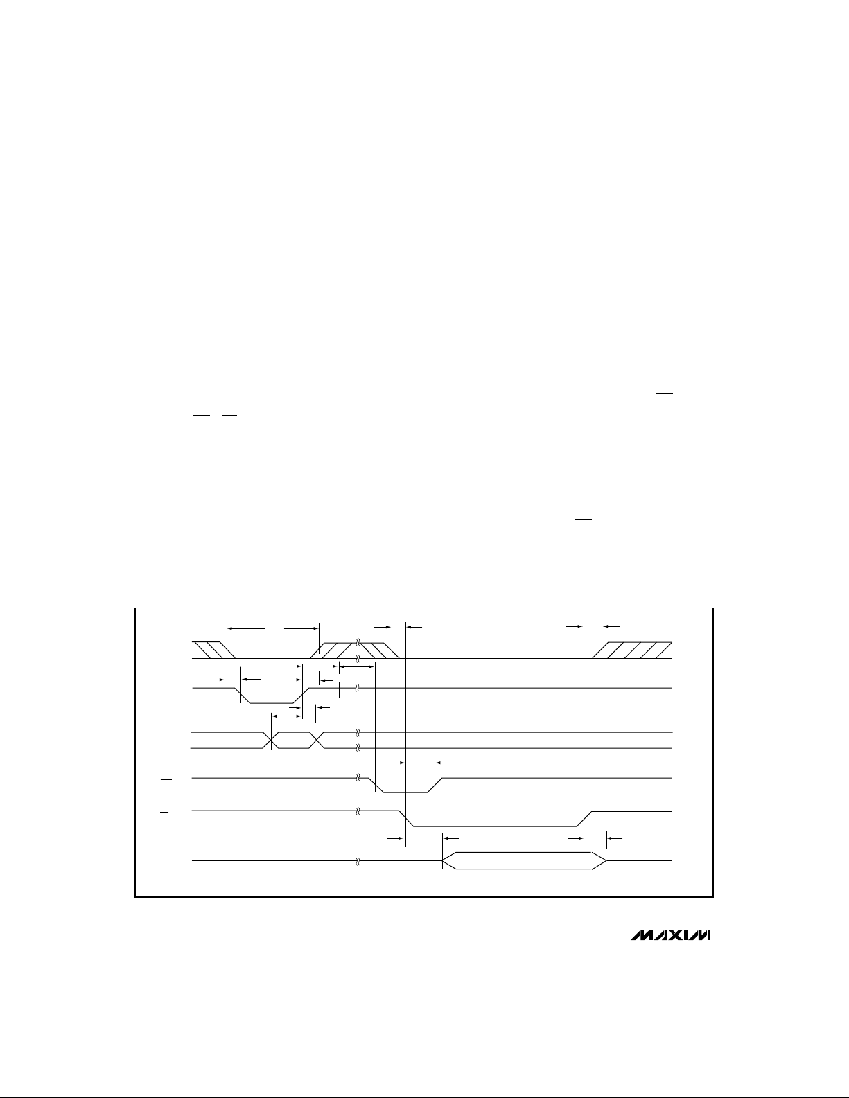
Internal Acquisition
Select internal acquisition by writing the control byte with
the ACQMOD bit cleared (ACQMOD = 0). This causes
the write pulse to initiate an acquisition interval whose
t
CS
duration is internally timed. Conversion starts when this
six-clock-cycle acquisition interval (3µs with f
CLK
2MHz) ends (see Figure 5).
External Acquisition
Use the external acquisition timing mode for precise control of the sampling aperture and/or independent control
of acquisition and conversion times. The user controls
acquisition and start-of-conversion with two separate
write pulses. The first pulse, written with ACQMOD = 1,
starts an acquisition interval of indeterminate length. The
second write pulse, written with ACQMOD = 0, terminates acquisition and starts conversion on WR’s rising
edge (Figure 6). However, if the second control byte
contains ACQMOD = 1, an indefinite acquisition interval
is restarted.
The address bits for the input mux must have the same
values on the first and second write pulses. Power-down
mode bits (PD0, PD1) can assume new values on the
second write pulse (see
Power-Down Mode
section).
How to Read a Conversion
A standard interrupt signal, INT, is provided to allow the
device to flag the µP when the conversion has ended
and a valid result is available. INT goes low when conversion is complete and the output data is ready
(Figures 5 and 6). It returns high on the first read cycle
or if a new control byte is written.
t
t
CSRS
CSRH
=
CS
t
CSWS
WR
D7–D0
INT
RD
DOUT
Figure 5. Conversion Timing Using Internal Acquisition Mode
10 ______________________________________________________________________________________
t
t
DS
WR
CONTROL
BYTE
ACQMOD ="0"
t
ACQI
t
t
DH
CSWH
t
CONV
t
INT1
t
D0
DATA VALID
t
TR
HIGH-ZHIGH-Z

Multirange, Single +5V, 12-Bit DAS
with 12-Bit Bus Interface
MAX196/MAX198
t
CS
CS
t
CSWS
WR
D7–D0
INT
RD
DOUT
Figure 6. Conversion Timing Using External Acquisition Mode
t
DS
ACQMOD = "1"
t
WR
CONTROL
BYTE
t
t
CSHW
DH
t
ACQI
CONTROL
BYTE
ACQMOD = "0"
Clock Modes
The MAX196/MAX198 operate with either an internal or
an external clock. Control bits (D6, D7) select either
internal or external clock mode. Once the desired clock
mode is selected, changing these bits to program
power-down will not affect the clock mode. In each
mode, internal or external acquisition can be used. At
power-up, external clock mode is selected.
Internal Clock Mode
Select internal clock mode to free the µP from the
burden of running the SAR conversion clock. To select
this mode, write the control byte with D7 = 0 and D6 =
1. A 100pF capacitor between the CLK pin and ground
sets this frequency to 1.56MHz nominal. Figure 7
shows a linear relationship between the internal clock
period and the value of the external capacitor used.
External Clock Mode
Select external clock mode by writing the control byte
with D7 = 0 and D6 = 0. Figure 8 shows CLK and WR
timing relationships in internal and external acquisition
modes, with an external clock. A 100kHz to 2.0MHz
external clock with 45% to 55% duty cycle is required for
proper operation. Operating at clock frequencies lower
than 100kHz will cause a voltage droop across the hold
capacitor, and subsequently degrade performance.
t
CSRS
t
CONV
t
INT1
t
D0
DATA VALID
2000
1500
1000
500
INTERNAL CLOCK PERIOD (ns)
0
0 50 250 350
100 150 200 300
CLOCK PIN CAPACITANCE (pF)
Figure 7. Internal Clock Period vs. Clock Pin Capacitance
t
CSRH
t
TR
______________________________________________________________________________________ 11

Multirange, Single +5V, 12-Bit DAS
with 12-Bit Bus Interface
ACQUISITION STARTS
CLK
t
CWS
WR
WR GOES HIGH WHEN CLK IS HIGH
CLK
ACQMOD = "0"
t
CWH
ACQUISITION STARTS
MAX196/MAX198
WR
ACQMOD = "0"
Figure 8a. External Clock and WR Timing (Internal Acquisition Mode)
ACQUISITION STARTS
CLK
t
DH
WR
ACQMOD = "1"
ACQUISITION STARTS
WR GOES HIGH WHEN CLK IS LOW
WR GOES HIGH WHEN CLK IS HIGH
ACQUISITION ENDS
ACQUISITION ENDS
ACQUISITION ENDS
ACQUISITION ENDS
t
CWS
ACQMOD = "0"
CONVERSION STARTS
CONVERSION STARTS
CONVERSION STARTS
CONVERSION STARTS
CLK
t
t
DH
WR
ACQMOD = "1"
WR GOES HIGH WHEN CLK IS LOW
CWH
ACQMOD = "0"
Figure 8b. External Clock and WR Timing (External Acquisition Mode)
12 ______________________________________________________________________________________

Multirange, Single +5V, 12-Bit DAS
with 12-Bit Bus Interface
__________Applications Information
Power-On Reset
At power-up, the internal power-on reset circuitry sets
INT high and puts the device in normal operation/external clock mode. This state is selected to keep the internal clock from loading the external clock driver when
the part is used in external clock mode.
Internal or External Reference
The MAX196/MAX198 can operate with either an internal or external reference. An external reference can be
connected to either the REF pin or the REFADJ pin
(Figure 9).
To use the REF input directly, disable the internal buffer
by tying REFADJ to VDD. Using the REFADJ input eliminates the need to buffer the reference externally. When
the reference is applied at REFADJ, bypass REFADJ with
a 0.01µF capacitor to AGND.
The REFADJ internal buffer gain is trimmed to 1.6384 to
provide 4.096V at the REF pin from a 2.5V reference.
Internal Reference
The internally trimmed 2.50V reference is gained
through the REFADJ buffer to provide 4.096V at REF.
Bypass the REF pin with a 4.7µF capacitor to AGND
and the REFADJ pin with a 0.01µF capacitor to AGND.
The internal reference voltage is adjustable to ±1.5%
(±65 LSBs) with the reference-adjust circuit of Figure 1.
External Reference
At REF and REFADJ, the input impedance is a minimum of 10kΩ for DC currents. During conversions, an
external reference at REF must be able to deliver
400µA DC load currents, and must have an output
impedance of 10Ω or less. If the reference has higher
output impedance or is noisy, bypass it close to the
REF pin with a 4.7µF capacitor to AGND.
With an external reference voltage of less than 4.096V
at the REF pin or less than 2.5V at the REFADJ pin, the
increase in the ratio of the RMS noise to the LSB value
(FS / 4096) results in performance degradation (loss of
effective bits).
Power-Down Mode
To save power, you can put the converter into lowcurrent shutdown mode between conversions. Two
programmable power-down modes are available:
STBYPD and FULLPD. Select STBYPD or FULLPD by
programming PD0 and PD1 in the input control byte.
When power-down is asserted, it becomes effective
only after the end of conversion. In all power-down
modes, the interface remains active and conversion
4.096V
REF
26
MAX196
MAX198
AV = 1.638
10k
2.5V
Figure 9a. Internal Reference
REF
MAX196
MAX198
A
= 1.638
V
10k
2.5V
Figure 9b. External Reference, Reference at REF
REF
MAX196
MAX198
A
= 1.638
V
10k
2.5V
Figure 9c. The external reference overdrives the internal reference.
4.7µF
C
REF
25REFADJ
0.01µF
26
25REFADJ
26
25REFADJ
4.096V
4.7µF
C
REF
V
4.096V
DD
4.7µF
C
REF
0.01µF
2.5V
MAX196/MAX198
______________________________________________________________________________________ 13
Multirange, Single +5V, 12-Bit DAS
with 12-Bit Bus Interface
results may be read. Input overvoltage protection is
active in all power-down modes. The device returns to
normal operation on the first WR falling edge during
write operation.
Choosing Power-Down Modes
The bandgap reference and reference buffer remain
active in STBYPD mode, maintaining the voltage on the
4.7µF capacitor at the REF pin. This is a “DC” state that
does not degrade after power-down of any duration.
Therefore, you can use any sampling rate with this
mode, without regard to start-up delays.
However, in FULLPD mode, only the bandgap reference is active. Connect a 33µF capacitor between REF
and AGND to maintain the reference voltage between
conversions and to reduce transients when the buffer is
MAX196/MAX198
enabled and disabled. Throughput rates down to 1ksps
can be achieved without allotting extra acquisition time
for reference recovery prior to conversion. This allows
conversion to begin immediately after power-down
ends. If the discharge of the REF capacitor during
FULLPD exceeds the desired limits for accuracy (less
OUTPUT CODE
11... 111
11... 110
11... 101
FULL-SCALE
TRANSITION
1 LSB =
4096
than a fraction of an LSB), run a STBYPD power-down
cycle prior to starting conversions. Take into account
that the reference buffer recharges the bypass capacitor at an 80mV/ms slew rate, and add 50µs for settling
time. Throughput rates of 10ksps offer typical supply
currents of 470µA, using the recommended 33µF
capacitor value.
Auto-Shutdown
Selecting STBYPD on every conversion automatically
shuts the MAX196/MAX198 down after each conversion
without requiring any start-up time on the next conversion.
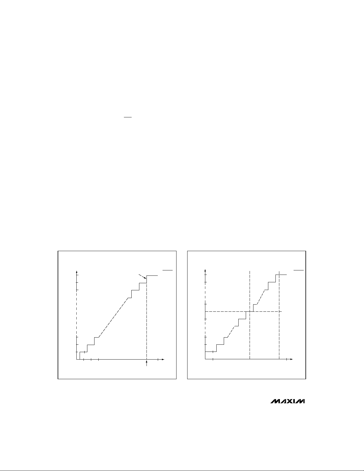
Transfer Function
Output data coding for the MAX196/MAX198 is binary
in unipolar mode with 1LSB = (FS / 4096) and twoscomplement binary in bipolar mode with 1LSB = [(2 x
) / 4096]. Code transitions occur halfway between
|FS|
successive-integer LSB values. Figures 10 and 11
show the input/output (I/O) transfer functions for unipolar and bipolar operations, respectively. For full-scale
(FS) values, refer to Table 1.
FS
OUTPUT CODE
011... 111
011... 110
1 LSB =
2FS
4096
000... 001
000... 000
111... 111
00... 011
00... 010
00... 001
00... 000
0
123
INPUT VOLTAGE (LSB)
Figure 10. Unipolar Transfer Function
14 ______________________________________________________________________________________
FS -
3
/2 LSB
FS
100... 010
100... 001
100... 000
-FS
Figure 11. Bipolar Transfer Function
0V +FS - 1 LSB
INPUT VOLTAGE (LSB)

Multirange, Single +5V, 12-Bit DAS
with 12-Bit Bus Interface
Careful printed circuit board layout is essential for best
Layout, Grounding, and Bypassing
system performance. For best performance, use a
ground plane. To reduce crosstalk and noise injection,
keep analog and digital signals separate. Digital
ground lines can run between digital signal lines to
minimize interference. Connect analog grounds and
DGND in a star configuration to AGND. For noise-free
operation, ensure the ground return from AGND to the
supply ground is low impedance and as short as possible. Connect the logic grounds directly to the supply
ground. Bypass VDDwith 0.1µF and 4.7µF capacitors
to AGND to minimize high- and low-frequency fluctuations. If the supply is excessively noisy, connect a 5Ω
resistor between the supply and VDD, as shown in
Figure 12.
+5V
R* = 5Ω
* OPTIONAL
** CONNECT AGND AND DGND WITH A GROUND PLANE OR A SHORT TRACE
4.7µF
0.1µF
V
DD
Figure 12. Power-Supply Grounding Connection
MAX196
MAX198
SUPPLY
**
GND
+5V
DGNDAGND
DGND
DIGITAL
CIRCUITRY
_________________________________________________________Functional Diagram
REF REFADJ
CH5
CH4
CH3
CH2
CH1
CH0
CLK
WR
INT
10k
COMP
12
REGISTER
12
D0–D11
AV =
1.638
SIGNAL
CONDITIONING
BLOCK
&
OVERVOLTAGE
TOLERANT
MUX
CLOCK
CS
RD
CONTROL LOGIC
&
LATCHES
T/H
CHARGE REDISTRIBUTION
12-BIT DAC
8
THREE-STATE, BIDIRECTIONAL
I/O INTERFACE
SUCCESSIVE-
APPROXIMATION
12-BIT DATA BUS
MAX196
MAX198
+2.5V
REFERENCE
V
DD
AGND
DGND
MAX196/MAX198
______________________________________________________________________________________ 15

Multirange, Single +5V, 12-Bit DAS
with 12-Bit Bus Interface
_Ordering Information (continued)
PIN-PACKAGETEMP. RANGEPART
Dice*0°C to +70°CMAX196BC/D
MAX196AENI
MAX196BENI
MAX198ACNI
-40°C to +85°C
-40°C to +85°CMAX196AEWI
MAX196/MAX198
MAX198ACWI
MAX198ACAI
MAX198BCAI
MAX198AENI
MAX198BENI
* Dice are specified at TA= +25°C, DC parameters only.
** Contact factory for availability and processing to MIL-STD-883.
0°C to +70°C
0°C to +70°CMAX198BCWI
0°C to +70°C
0°C to +70°CMAX198BC/D
-40°C to +85°C
-40°C to +85°CMAX198AEWI
28 Narrow Plastic DIP-40°C to +85°C
28 Narrow Plastic DIP
28 Wide SO
28 Wide SO-40°C to +85°CMAX196BEWI
28 SSOP-40°C to +85°CMAX196AEAI
28 SSOP-40°C to +85°CMAX196BEAI
28 Narrow Ceramic SB**-55°C to +125°CMAX196AMYI
28 Narrow Ceramic SB**-55°C to +125°CMAX196BMYI
28 Narrow Plastic DIP0°C to +70°C
28 Narrow Plastic DIP0°C to +70°CMAX198BCNI
28 Wide SO
28 Wide SO
28 SSOP0°C to +70°C
28 SSOP
Dice*
28 Narrow Plastic DIP-40°C to +85°C
28 Narrow Plastic DIP
28 Wide SO
28 Wide SO-40°C to +85°CMAX198BEWI
28 SSOP-40°C to +85°CMAX198AEAI
28 SSOP-40°C to +85°CMAX198BEAI
28 Narrow Ceramic SB**-55°C to +125°CMAX198AMYI
28 Narrow Ceramic SB**-55°C to +125°CMAX198BMYI
___________________Chip Topography
V
V
CLKD11
CS
D10
D9
D8
D7
D6
D5
D4
D3
D2
0.144"
(3.659mm)
TRANSISTOR COUNT: 2956
SUBSTRATE CONNECTED TO GND
DD
CH0
CC
WRDGND
RD
INT
REF
0.231"
(5.870mm)
REFADJ
CH5
CH4
CH3
CH2
CH1D0D1AGND
Maxim cannot assume responsibility for use of any circuitry other than circuitry entirely embodied in a Maxim product. No circuit patent licenses are
implied. Maxim reserves the right to change the circuitry and specifications without notice at any time.
16
__________________Maxim Integrated Products, 120 San Gabriel Drive, Sunnyvale, CA 94086 (408) 737-7600
© 1995 Maxim Integrated Products Printed USA is a registered trademark of Maxim Integrated Products.
 Loading...