

Page 1
General Description
The MAX1966/MAX1967 are voltage-mode pulse-widthmodulated (PWM), step-down DC-DC controllers that
are ideal for a variety of cost-sensitive applications.
They drive low-cost N-MOSFETs for both the high-side
switch and synchronous rectifier and require no external
Schottky power diode or current-sense resistor. Shortcircuit and current-limit protection is provided by sensing the drain-to-source voltage on the low-side FET.
Both devices can supply outputs as low as 0.8V and are
well suited for DSP cores and other low-voltage logic.
The MAX1966 has an input range of 2.7V to 5.5V while
the MAX1967 has an input range of 2.7V to 28V. In
ultra-low-cost designs, the MAX1966/MAX1967 can
provide efficiency exceeding 90% and can achieve
95% efficiency with optimized component selection.
The MAX1966/MAX1967 operate at 100kHz and accommodate aluminum electrolytic capacitors and powdered-iron core magnetics in minimum-cost designs.
They also provide excellent performance with high-performance surface-mount components. The MAX1966 is
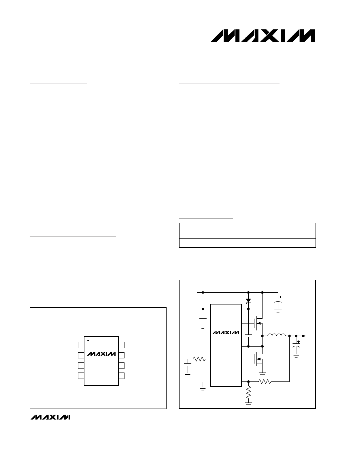
available in a low-cost 8-pin SO package. The MAX1967
is available in a 10-pin µMAX package.
Applications
Features
♦ Cost-Optimized Design
♦ No Schottky Diode or Current-Sense Resistor
Required
♦ >95% Efficiency
♦ Low-Cost External Components
♦ All N-Channel FET Design
♦ 2.7V to 5.5V Input Range (MAX1966)
♦ 2.7V to 28V Input Range (MAX1967)
♦ 0.8V Feedback for Low-Voltage Outputs
♦ 100kHz Switching Frequency Accommodates
Low-Cost Components
♦ Thermal Shutdown
♦ Output Current-Limit and Short-Circuit Protection
MAX1966/MAX1967
Low-Cost Voltage-Mode PWM
Step-Down Controllers
________________________________________________________________ Maxim Integrated Products 1
Pin Configurations
Ordering Information
MAX1966
V
OUT
2.7V TO
5.5V INPUT
VIN
COMP/EN
GND
BST
DH
LX
DL
FB
Typical Operating Circuit
19-2286; Rev 1; 9/03
For pricing, delivery, and ordering information, please contact Maxim/Dallas Direct! at
1-888-629-4642, or visit Maxim’s website at www.maxim-ic.com.
Pin Configurations continued at end of data sheet.
Set-Top Boxes
Graphic Card Supplies
xDSL Modems and
Routers
Cable Modems and
Routers
Telecom Power Supplies
Networking Power
Supplies
Termination Supplies
PART TEMP RANGE PIN-PACKAGE
MAX1966ESA -40°C to +85°C 8 SO
MAX1967EUB -40°C to +85°C 10 µMAX
TOP VIEW
1
BST
2
MAX1966
3
FB
4
SO
87DH
6
5
LXCOMP/EN
GND
DLVIN
Page 2
MAX1966/MAX1967
Low-Cost Voltage-Mode PWM
Step-Down Controllers
2 _______________________________________________________________________________________
ABSOLUTE MAXIMUM RATINGS
ELECTRICAL CHARACTERISTICS
(VIN = VL = VCC = 5V (MAX1967), VIN = 5V (MAX1966), TA= -40°C to +85°C (Note 1), unless otherwise noted. Typical values are at
T
A
= +25°C.)
Stresses beyond those listed under “Absolute Maximum Ratings” may cause permanent damage to the device. These are stress ratings only, and functional
operation of the device at these or any other conditions beyond those indicated in the operational sections of the specifications is not implied. Exposure to
absolute maximum rating conditions for extended periods may affect device reliability.
(All Voltages Referenced to GND, Unless Otherwise Noted)
VIN to GND (MAX1966)............................................-0.3V to +6V
VIN to GND (MAX1967)..........................................-0.3V to +30V
VCC to GND (MAX1967)..........-0.3V, lower of 6V or (VIN+ 0.3V)
FB to GND ................................................................-0.3V to +6V
DL, COMP/EN to GND (MAX1966) ................-0.3V to V
IN
+ 0.3V
VL, DL, COMP/EN to GND (MAX1967).........-0.3V to V
CC
+ 0.3V
BST to LX..................................................................-0.3V to +6V
DH to LX........................................................-0.3V to BST + 0.3V
VL Short to GND (MAX1967) ....................................................5s
RMS Input Current (any pin).............................................±50mA
Continuous Power Dissipation (T
A
= +70°C)
8-Pin SO (derate 5.88mW/°C above +70°C)................471mW
10-Pin µMAX (derate 5.6mW/°C above +70°C) ...........444mW
Operating Temperature Range ...........................-40°C to +85°C
Junction Temperature......................................................+150°C
Storage Temperature Range .............................-65°C to +150°C
Lead Temperature (soldering, 10s) .................................+300°C
MAX1967 VIN Operating Range 4.9 28 V
MAX1967 Operating Range with
VIN = VL
MAX1966 VIN Operating Range 2.7 5.5 V
MAX1967 VL Undervoltage
Lockout (UVLO) Trip Level
MAX1966 VIN UVLO
Trip Level
Operating Supply Current FB = 0.88V, no switching 0.7 3 mA
V L Outp ut V ol tag e ( M AX 1967 Onl y)
Thermal Shutdown (Note 1) Rising temperature, typical hysteresis = 10°C 160 °C
OSCILLATOR
Frequency f
Minimum Duty Cycle 10 %
Maximum Duty Cycle 90 95 %
SOFT-START
Digital Ramp Period
Soft-Start Levels
ERROR AMPLIFIER
FB Regulation Voltage
(MAX1967)
FB Regulation Voltage
(MAX1966)
FB to COMP/EN Gain 4000 V/V
PARAMETER SYMBOL CONDITIONS MIN TYP MAX UNITS
Rising and falling edge, hysteresis = 2% 2.35 2.53 2.66 V
Rising and falling edge, hysteresis = 2% 2.35 2.53 2.66 V
5.5V < VIN < 28V, 1mA < I
FB = 0.88V
OSC
0°C to +85°C 82 102 124
-40°C to +85°C 79 102 127
Internal 6-bit DAC for converter to ramp from
0 to full output voltage
2.7V < VCC < 5.5V, 0°C to +85°C 0.787 0.800 0.815
2.7V < VCC < 5.5V, -40°C to +85°C 0.782 0.800 0.815
2.7V < VIN < 5.5V, 0°C to +85°C 0.787 0.800 0.815
2.7V < VIN < 5.5V, -40°C to +85°C 0.782 0.800 0.815
< 25mA,
VL
2.7 5.5 V
4.67 5 5.3 V
1024 /
f
OSC
V
/
OUT
64
kHz
s
V
V
V
Page 3
MAX1966/MAX1967
Low-Cost Voltage-Mode PWM
Step-Down Controllers
_______________________________________________________________________________________ 3
ELECTRICAL CHARACTERISTICS (continued)
(VIN = VL = VCC = 5V (MAX1967), VIN = 5V (MAX1966), TA= -40°C to +85°C, unless otherwise noted. Typical values are at
T
A
= +25°C.)
Note 1: Specifications to -40°C are guaranteed by design and not production tested.
Note 2: Thermal shutdown disables the buck regulator when the die reaches this temperature. Soft-start is reset and COMP/EN is
discharged to zero. In the MAX1967, the VL regulator remains on during thermal shutdown.
FB to COMP/EN
Transconductance
FB Input Bias Current V
COMP/EN Source Current V
Current-Limit Threshold Voltage
(Across Low-Side NFET)
MOSFET DRIVERS
Break-Before-Make Time 30 ns
DH On-Resistance in Low State V
DH On-Resistance in High State V
DH Peak Source and Sink
Current
DL On-Resistance in Low State I
DL On-Resistance in High State I
DL Source Current VDL = 2.5V 1 A
DL Sink Current VDL = 2.5V 2 A
Maximum Total (DH + DL)
Average Source Current
BST Leakage Current V
LX Leakage Current V
PARAMETER SYMBOL CONDITIONS MIN TYP MAX UNITS
-5µA < I
COMP/EN
= 0.880V 3 100 nA
FB
COMP/EN
LX to GND -340 -305 -270 mV
= 5V, VLX = 0, I
BST
= 5V, VLX = 0, I
BST
V
= 5V, VLX = 0, DH = 2.5V 1 A
BST
= -50mA 1.1 2.5 Ω
DL
= 50mA 2.5 5.5 Ω
DL
= 5V, VLX = 0 25 mA
V
BST
= 33V, V
BST
= 33V, V
BST
< 5µA 70 108 160 µS
= 0 15 46 100 µA
= -50mA 1.6 4 Ω
DH
= 50mA 2.5 5.5 Ω
DH
= 28V 0 50 µA
LX
= 28V 33 100 µA
LX
Page 4
MAX1966/MAX1967
Low-Cost Voltage-Mode PWM
Step-Down Controllers
4 _______________________________________________________________________________________
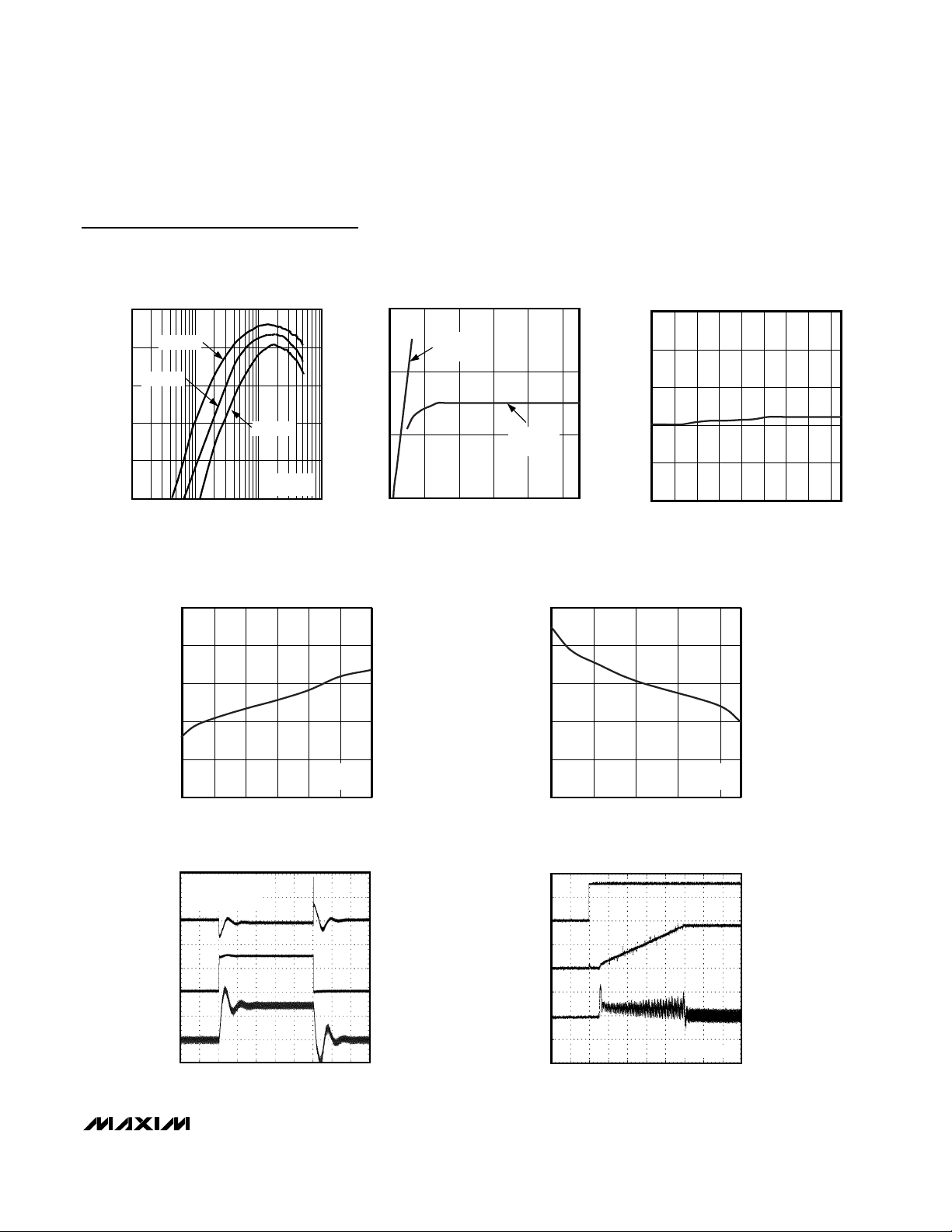
Typical Operating Characteristics
(TA = +25°C, unless otherwise noted.)
100
50
0.01 0.1 1 10
EFFICIENCY vs. LOAD CURRENT
(1.2V/3A)
60
MAX1966 toc01
LOAD CURRENT (A)
EFFICIENCY (%)
70
80
90
VIN = 5.0V
VIN = 3.3V
MAX1966
FIGURE 1
100
50
0.01 0.1 1 10
EFFICIENCY vs. LOAD CURRENT (1.8V/3A)
MAX1966
60
MAX1966 toc02
LOAD CURRENT (A)
EFFICIENCY (%)
70
80
90
VIN = 5.0V
VIN = 3.3V
MAX1966
FIGURE 1
100
50
0.01 0.1 1 10
EFFICIENCY vs. LOAD CURRENT (1.2V/5A)
MAX1966
60
MAX1966 toc03
LOAD CURRENT (A)
EFFICIENCY (%)
70
80
90
VIN = 5.0V
VIN = 5.0V
VIN = 3.3V
VIN = 3.3V
MAX1966
FIGURE 1
100
50
0.01 0.1 1 10
EFFICIENCY vs. LOAD CURRENT (1.8V/5A)
MAX1966
60
MAX1966 toc04
LOAD CURRENT (A)
EFFICIENCY (%)
70
80
90
VIN = 5.0V
VIN = 3.3V
MAX1966
FIGURE 1
100
50
0.01 0.1 1 10
EFFICIENCY vs. LOAD CURRENT (1.2V/3A)
MAX1967
60
MAX1966 toc05
LOAD CURRENT (A)
EFFICIENCY (%)
70
80
90
VIN = 5V
VIN = 12V
MAX1967
FIGURE 2
100
50
0.01 0.1 1 10
EFFICIENCY vs. LOAD CURRENT (1.8V/3A)
MAX1967
60
MAX1966 toc06
LOAD CURRENT (A)
EFFICIENCY (%)
70
80
90
VIN = 5V
VIN = 12V
MAX1967
FIGURE 2
100
50
0.01 0.1 1 10
EFFICIENCY vs. LOAD CURRENT (3.3V/3A)
MAX1967
60
MAX1966 toc07
LOAD CURRENT (A)
EFFICIENCY (%)
70
80
90
VIN = 5V
V
IN
= 12V
MAX1967
FIGURE 2
100
50
0.01 0.1 1 10
EFFICIENCY vs. LOAD CURRENT (1.2V/5A)
MAX1967
60
MAX1966 toc08
LOAD CURRENT (A)
EFFICIENCY (%)
70
80
90
VIN = 5V
VIN = 5V
VIN = 12V
VIN = 20V
MAX1967
FIGURE 2
100
50
0.01 0.1 1 10
EFFICIENCY vs. LOAD CURRENT (1.8V/5A)
MAX1967
60
MAX1966 toc09
LOAD CURRENT (A)
EFFICIENCY (%)
70
80
90
VIN = 5V
VIN = 12V
VIN = 20V
MAX1967
FIGURE 2
Page 5
MAX1966/MAX1967
Low-Cost Voltage-Mode PWM
Step-Down Controllers
_______________________________________________________________________________________ 5
Typical Operating Characteristics (continued)
(TA = +25°C, unless otherwise noted.)
0
2
4
6
8
10
41491924
MAX1967 SUPPLY CURRENT
vs. INPUT VOLTAGE
MAX1966 toc14
INPUT VOLTAGE (V)
SUPPLY CURRENT (mA)
MAX1967
V
OUT
= 3.3V
0
2
4
6
8
10
2.5 4.03.53.0 4.5 5.55.0
MAX1966 SUPPLY CURRENT
vs. INPUT VOLTAGE
MAX1966 toc13
INPUT VOLTAGE (V)
SUPPLY CURRENT (mA)
MAX1966
V
OUT
= 1.8V
EFFICIENCY vs. LOAD CURRENT (3.3V/5A)
MAX1967
100
90
80
70
EFFICIENCY (%)
60
50
VIN = 5V
VIN = 12V
VIN = 24V
MAX1967
FIGURE 2
0.01 0.1 1 10
LOAD CURRENT (A)
MAX1966 toc10
FREQUENCY (kHz)
FREQUENCY vs. INPUT VOLTAGE
104
MAX1966
= 1.8V
V
OUT
102
100
98
2.5 7.0 16.011.5 20.5 25.0
INPUT VOLTAGE (V)
MAX1967
V
OUT
= 3.3V
MAX1966 toc11
FREQUENCY (kHz)
FREQUENCY vs. TEMPERATURE
130
120
110
100
90
80
-40 -25 20 355-10 50 8065
TEMPERATURE (°C)
MAX1966 toc12
LOAD STEP RESPONSE
VIN = 5.0V, V
L = 22µH
= 0.1 TO 3A
I
LOAD
V
OUT
I
OUT
INDUCTOR
CURRENT
OUT
= 1.8V
400ms/div
MAX1966 toc15
200mV/div
2A/div
2A/div
V
OUT
INDUCTOR
CURRENT
START-UP WAVEFORM
MAX1966 toc16
V
IN
NO LOAD
2ms/div
2V/div
1V/div
1A/div
Page 6

MAX1966/MAX1967
Low-Cost Voltage-Mode PWM
Step-Down Controllers
6 _______________________________________________________________________________________
Typical Operating Characteristics (continued)
(TA = +25°C, unless otherwise noted.)
1A/div
1V/div
2V/div
INDUCTOR
CURRENT
VOUT
VIN
10ms/div
SHUTDOWN WAVEFORMS
MAX1966 toc18
NO LOAD
Pin Description
MAX1966 toc17
I
OUT
VIN = 5.0V
= 1.8V
V
IN
L = 22µF
PIN
MAX1966 MAX1967
1 10 BST Positive Supply of DH Driver. Connect 0.1µF ceramic capacitor between BST and LX.
2 1 COMP/EN
3 2 FB Feedback Input. Connect a resistive divider network to set V
— 3 VCC Internal Chip Supply. Connect to VL via a 10Ω resistor.
4 4 VIN
— 5VL
5 6 DL Low-Side External MOSFET Gate-Driver Output. DL swings from VL to GND.
6 7 GND Ground and Negative Current-Sense Input
78LX
8 9 DH High-Side External MOSFET Gate-Driver Output. DH swings from BST to LX.
NAME FUNCTION
Compensation Pin. Pulling COMP/EN low with an open-collector or open-drain device
turns off the output.
Power Supply for LDO Regulator in the MAX1967 and Chip Supply for the MAX1966.
Bypass with a ceramic capacitor to ground (see application circuit).
Output of Internal 5V LDO. Bypass with a 2.2µF capacitor to GND, or if VIN < 5.5,
connect VL to VIN and bypass with a 0.1µF capacitor to GND.
Inductor Switching Node. L
driver.
D
H
is used for both current limit and the return supply of the
X
. FB threshold is 0.8V.
OUT
Page 7

MAX1966/MAX1967
Low-Cost Voltage-Mode PWM
Step-Down Controllers
_______________________________________________________________________________________ 7
Detailed Description
The MAX1966/MAX1967 are BiCMOS switch-mode
power-supply controllers designed to implement simple, buck-topology regulators in cost-sensitive applications. The main power-switching circuit consists of two
N-channel MOSFETs (or a dual MOSFET), an inductor,
and input and output filter capacitors. An all N-channel
synchronous-rectified design provides high efficiency
at reduced cost. Gate drive for the N-channel high-side
switch is provided by a flying capacitor boost circuit
that uses a 0.1µF capacitor connected to BST.
Major circuit blocks of the MAX1966/MAX1967 are
shown in Figures 1 and 2:
• Control Logic
• Gate Driver Outputs
• Current-Limit Comparator
• Clock Generator
• Ramp Generator
• Error Amplifier
• Error Comparator
• Soft-Start
• 5V Linear Regulator (MAX1967)
• 800mV Reference
• Thermal Shutdown
In the MAX1996, most blocks are powered from VIN. In
the MAX1967, an internal 5V linear regulator steps
down the input voltage to supply both the IC and the
gate drivers. The synchronous-rectified gate driver is
directly powered from 5V VL, while the high-side-switch
gate driver is indirectly powered from VLplus an external diode-capacitor boost circuit.
Resistorless Current Limit
The MAX1966/MAX1967 use the R
DS(ON)
of the lowside N-channel MOSFET to sense the current. This
eliminates the need for an external sense resistor usually placed in series with the output. The voltage measured across the low-side R
DS(ON)
is compared to a
fixed -305mV reference (Figures 1 and 2). The peak
inductor current limit is given by the equation below:
MOSFET Gate Drivers
The DH and DL drivers are optimized for driving
MOSFETs with low gate charge. An adaptive dead-time
circuit monitors the DL output and prevents the highside FET from turning on until the low-side MOSFET is
fully off. There must be a low-resistance, low-inductance
connection from the DL driver to the MOSFET gate for
the adaptive dead-time circuit to work properly.
Otherwise, the sense circuitry in the MAX1966/
MAX1967 detects the MOSFET gate as off while there
is charge left on the gate. Use very short, wide traces
measuring no less than 50mils to 100mils wide if the
MOSFET is 1in away from the MAX1966/MAX1967. The
same type of adaptive dead-time circuit monitors the
DH off edge. The same recommendations apply for the
gate connection of the high-side MOSFET.
The internal pulldown transistor that drives DL low is
robust, with a 1.1Ω typical on-resistance. This helps
prevent DL from being pulled up due to capacitive coupling from the drain to the gate of the low-side synchronous-rectifier MOSFET during the fast rise time of the
inductor node. The gate drivers are capable of driving
up to 1A. Use MOSFETs with combined total gate
charge of less than 200nC and a maximum V
TH
of 3.5V.
Internal Soft-Start
The MAX1966/MAX1967 feature an internally set softstart function that limits inrush current. It accomplishes
this by ramping the internal reference input to the controller transconductance amplifier from 0 to the 0.8V
reference voltage. The ramp time is 1024 oscillator
cycles that begins when initial power is applied. At the
nominal 100kHz switching rate, the soft-start ramp is
approximately 10ms. The soft-start does not function if
the MAX1966/MAX1967 are shut down by pulling
COMP/EN low.
High-Side Gate-Drive Supply (BST)
Gate-drive voltage for the high-side N-channel switch is
generated by a flying-capacitor boost circuit (Figures 3
and 4). The flying capacitor is connected between BST
and LX.
On startup, the synchronous rectifier (low-side MOSFET) forces LX to ground and charges the boost
capacitor to 5V. On the second half-cycle, the
MAX1966/MAX1967 turn on the high-side MOSFET by
closing an internal switch between BST and DH. This
provides the necessary gate-to-source voltage to drive
the high-side FET gate above its source at the input
voltage.
Internal 5V Linear Regulator
(MAX1967)
All MAX1967 functions are internally powered from an
on-chip, low-dropout 5V regulator. The MAX1967 has a
maximum regulator input voltage (V
VIN
) of 28V. The
VCC pin must be connected to VL through a 10Ω resistor and VL must be bypassed with a 2.2µF capacitor to
GND. For operation at V
VIN
< 5V, connect VL to VIN
ImVR
= 305 /
PEAK DS ON
()
Page 8

MAX1966/MAX1967
Low-Cost Voltage-Mode PWM
Step-Down Controllers
8 _______________________________________________________________________________________
Figure 3. MAX1966 Typical Application
MAX1967
5V TO
28V INPUT
VIN
COMP/EN
GND
BST
VCC
VL
DH
LX
DL
FB
R2
R1
V
OUT
C3
C4
L1
C2
C5
D1
C7
N1
N2
C6
R3
C1
R4
10Ω
10Ω
Figure 4. MAX1967 Typical Application
TEMPERATURE
SHUTDOWN
CONTROL
LOGIC
RAMP
GENERATOR
SOFT-START
100kHZ
CLOCK
GENERATOR
DH
DL
GND
CURRENT-LIMIT
COMPARATOR
ERROR
COMPARATOR
ERROR
AMPLIFIER
-305mV
LX
BST
VIN
COMP/EN
FB
800mV
REF
MAX1966
Figure 1. MAX1966 Functional Diagram
TEMPERATURE
SHUTDOWN
CONTROL
LOGIC
5V LINEAR
REGULATOR
RAMP
GENERATOR
SOFT-START
100kHZ
CLOCK
GENERATOR
DH
DL
GND
CURRENT-LIMIT
COMPARATOR
ERROR
COMPARATOR
ERROR
AMPLIFIER
-305mV
LX
BST
VIN
VL
COMP/EN
FB
V
CC
800mV
REF
INTERNAL
CHIP
SUPPLY
MAX1967
Figure 2. MAX1967 Functional Diagram
SEE TABLE 1 FOR COMPONENT VALUES. SEE TABLE 1 FOR COMPONENT VALUES.
2.7V TO
5.5V INPUT
C7
VIN
MAX1966
R3
COMP/EN
C6
GND
BST
DH
LX
DL
FB
D1
C1
N1
C5
N2
R1
R2
L1
C2
V
OUT
C4
C3
Page 9

MAX1966/MAX1967
Low-Cost Voltage-Mode PWM
Step-Down Controllers
_______________________________________________________________________________________ 9
and keep a 0.1µF capacitor between VL and GND
close to the chip. The VIN-to-VLdropout voltage is typically 70mV at 25mA current, so when V
VIN
is less than
5V, VVLis typically V
VIN
- 70mV.
The internal linear regulator can source a minimum of
25mA to supply the IC and power the low-side and
high-side FET drivers.
Duty-Factor Limitations for Low
V
OUT/VVIN
Ratios
The MAX1966/MAX1967s’ output voltage is adjustable
down to 0.8V. However, the minimum duty factor may
limit the ability to supply low-voltage outputs from highvoltage inputs. With high-input voltages, the required
duty factor is approximately:
where R
DS(ON)
x I
LOAD
is the voltage drop across the
synchronous rectifier. The MAX1966/MAX1967s’ minimum duty factor is 10%, so the maximum input voltage
(V
VIN(DFMAX)
) that can supply a given output voltage is:
If the circuit cannot attain the required duty factor dictated by the input and output voltages, the output voltage still remains in regulation. However, there may be
intermittent or continuous half-frequency operation as
the controller attempts to lower the average duty factor
by deleting pulses. This can increase output voltage
ripple and inductor current ripple, which increases
noise and reduces efficiency. Furthermore, circuit stability is not guaranteed.
Applications Information
Design Procedure
Component selection is primarily dictated by the following criteria:
1) Input Voltage Range: The maximum value
(V
VIN(MAX)
) must accommodate the worst-case
high-input voltage. The minimum value (V
VIN(MIN)
)
must account for the lowest input voltage after
drops due to connectors, fuses, and switches are
considered. In general, lower input voltages provide the best efficiency.
2) Maximum Load Current: There are two current val-
ues to consider. Peak load current (I
LOAD(MAX)
)
determines the instantaneous component stresses
and filtering requirements and is key in determining
output capacitor requirements. I
LOAD(MAX)
also
determines the required inductor saturation rating
and the design of the current-limit circuit. Continuous load current (I
LOAD
) determines the thermal
stresses, input capacitor, and MOSFETs, as well as
the RMS ratings of other heat-contributing components such as the inductor.
3) Inductor Value: This choice provides tradeoffs
between size, transient response, and efficiency.
Higher inductance value results in lower inductor
ripple current, lower peak current, lower switching
losses, and, therefore, higher efficiency at the cost
of slower transient response and larger size. Lower
inductance values result in large ripple currents,
smaller size, and poorer efficiency, while also providing faster transient response. Except for low-current applications, most circuits exhibit a good
balance between efficiency and economics with a
minimum inductor value that causes the circuit to
operate at the edge of continuous conduction
(where the inductor current just touches zero with
every cycle at maximum load). Inductor values lower
than this grant no further size-reduction benefit.
Table 1 shows representative values for some typical
applications up to 5A. With proper component selection, outputs of 20A or more are practical with the
MAX1966/MAX1967. The components listed in Table 1
were selected assuming a minimum cost design goal.
The MAX1966/MAX1967 can effectively operate with a
wide range of components.
Setting the Output Voltage
An output voltage between 0.8V and (0.9V x V
VIN
) can
be configured by connecting FBpin to a resistive
divider between the output and GND (Figures 3 and 4).
Select resistor R2 in the 1kΩ to 10kΩ range. R1 is then
given by:
where VFB= 0.8V.
Inductor Selection
Determine an appropriate inductor value with the following equation:
where LIR is the ratio of inductor ripple current to average continuous current at a minimum duty cycle.
Choosing LIR between 20% to 50% results in a good
VVRI
VR I V
+×
()
OUT DS ON LOAD VIN
VIN DFMAX OUT DS ON LOAD() ()
()
10
()
/
≤+ ×
LV
=×
OUT
V f LIR I
VIN OSC LOAD MAX
V
RR
12
OUT
V
FB
VV
−
()
IN OUT
×××
1=−
()
Page 10

MAX1966/MAX1967
Low-Cost Voltage-Mode PWM
Step-Down Controllers
10 ______________________________________________________________________________________
compromise between efficiency and economy. Choose
a low-loss inductor having the lowest possible DC
resistance. Ferrite-core-type inductors are often the
best choice for performance, however; the MAX1966/
MAX1967s’ 100kHz switching rate also allows the use
of powdered-iron cores in ultra-low-cost applications
where efficiency is not critical. With any core material,
the core must be large enough not to saturate at the
peak inductor current (I
PEAK
):
Setting the Current Limit
The MAX1966/MAX1967 provide current limit by sensing the voltage across the external low-side MOSFET.
The current-limit threshold voltage is nominally -305mV.
The MOSFET on-resistance required to allow a given
peak inductor current is:
or
in terms of actual output current.
A limitation of sensing current across MOSFET resistance is that current-limit threshold is not accurate
since the MOSFET R
DS(ON)
specification is not precise.
This type of current limit provides a coarse level of fault
protection. It is especially suited when the input source
is already current limited or otherwise protected.
However, since current-limit tolerance may be ±45%,
this method may not be suitable in applications where
this device’s current limit is the primary safety mechanism, or where accurate current limit is required.
Output Capacitor Selection
The output filter capacitor must have low enough equivalent series resistance (ESR) to meet output ripple and
load transient requirements, yet have high enough ESR
to satisfy stability requirements. In addition, the capacitance value must be high enough to absorb the inductor energy going from a full-load to no-load condition if
such load changes are anticipated in the system.
In applications where the output is subject to large load
transients, the output capacitor’s size depends primarily on how low an ESR is needed to prevent the output
from dipping too low under load transients. Ignoring the
sag due to finite capacitance:
In applications with less severe load steps, the output
capacitor’s size may then primarily depend on how low
an ESR is required to maintain acceptable output ripple:
The actual capacitance value required relates to the
physical size and technology needed to achieve low
ESR. Thus, the capacitor is usually selected by physical size, ESR, and voltage rating rather than by capacitance value. With current capacitor technology, once
the ESR requirement is satisfied, the capacitance is
usually also sufficient. When using a low-capacity filter
capacitor such as ceramic or polymer types, capacitor
size is usually determined by the capacitance needed
to prevent undershoot and overshoot voltages during
load transients. The overshoot voltage is given by:
Generally, once enough capacitance is added to meet
the overshoot requirement, undershoot at the rising
load edge is no longer a problem.
Stability and Compensation
To ensure stable operation, use the following compensation procedure:
1) Determine accaptable output ripple and select the
inductor and output capacitor values as outlined in
the Inductor Selection and Output Capacitor
Selection sections.
2) Check to make sure that output capacitor ESR zero
is less than f
OSC
/π. Otherwise, increase capaci-
tance until this condition is satisfied.
3) Select R3 value to set high-frequency error-amplifier gain so that the unity-gain frequency of the loop
occurs at the output ESR zero:
A good choice for R3is 50kΩ. Do not exceed 100kΩ.
R
ESR
II
=+
PEAK LOAD MAX LOAD MAX
() ()
LIR
2
×
I
R
ESR
RmVI
DS ON MAX PEAK()
/≤ 305
R
DS ON MAX
()
I
LOAD MAX
()
mV
305
≤×+
LIR
1
2
V
SOAR
R
3
−
80 10=×××
6
V
≤
I
LOAD MAX
≤
LIR I
LI
=
××
2
V
OUT
VR
VIN ESR
DIP
()
V
RIPPLE
×
VC
OUT OUT
LOAD MAX
×
PEAK
()
2
L
C
OUT
Ω
()
Page 11

4) Select compensation capacitor C6so that the error
amp zero is equal to the complex pole frequency
LC of the inductor and output capacitor:
Input Capacitor Selection
The input capacitor (C2) reduces noise injection and
the current peaks drawn from the input supply. The
source impedance to the input supply determines the
value of C2. High source impedance requires high
input capacitance. The input capacitor must meet the
ripple current requirement (I
RMS
) imposed by the
switching currents. The RMS input ripple current is
given by:
For optimal circuit reliability, choose a capacitor that
has less than a 10°C temperature rise at the peak ripple current.
Power MOSFET Selection
The MAX1966/MAX1967s’ step-down controller drives
two external logic-level N-channel MOSFETs. The key
selection parameters are:
1) On-resistance (R
DS(ON)
) of both MOSFETs for cur-
rent limit and efficiency
2) Current capability of V
L
(MAX1967 only) and gate
charge (Q
T
)
3) Voltage rating and maximum input voltage
MOSFET Power Dissipation
Worst-case conduction losses occur at the duty factor
extremes. For the high-side MOSFET, the worst-case
power dissipation due to resistance occurs at minimum
input voltage:
The following switching loss calculation for the highside N-FET provides an approximation, but is no substitute for evaluation:
where C
RSS
is the reverse transfer capacitance of N1
and I
GATE
is the peak gate-drive source/sink current
(1A typical). For the low-side N-FET (N2), the worstcase power dissipation occurs at maximum input voltage:
The low-side MOSFET on-resistance sets the
MAX1966/MAX1967 current limit. See the Setting the
Current Limit section for information on selecting lowside MOSFET R
DSON
. For designs supplying 5A or
less, it is often possible to combine the high-side and
low-side MOSFETs into a single package (usually an 8pin SO) as indicated in Table 1. For higher output applications, or those where efficiency is more important,
separate FETs are usually preferred.
Very-Low-Voltage Applications
The MAX1966/MAX1967 are extremely versatile controllers that can be used in a variety of applications
where high efficiency, high output power, and optimized cost are important. One alternate connection,
shown in Figure 5, is useful when a low-voltage supply
is to be stepped down to an even lower voltage at high
current. If an additional bias supply is available, it can
supply gate drive separately from the input power rail.
This can either improve efficiency, or allow lower cost
5V logic-level MOSFETs to be used in place of 3V
MOSFETs.
MAX1966/MAX1967
Low-Cost Voltage Mode PWM
Step-Down Controller
______________________________________________________________________________________ 11
Figure 5. Low Input Voltage Step-Down with Extra Bias Supply
for Gate Drive
LC
C
=×
6
OUT
R
3
II
RMS LOAD
=×
VVV
×−
OUT VIN OUT
()
V
VIN
P
D N RESISTIVE
1
V
OUT
=××
V
VIN MIN
()
2
IR
LOAD DS ON()
()
P
D N SWITCHING
1
I
LOAD
=× ××
I
GATE
VfC
VIN MAX OSC RSS(/ ) ( )
2
5V TO 28V FOR
GATE BIAS
VIN
MAX1967
COMP/EN
GND
VCC
BST
DH
VL
LX
DL
FB
R1
R2
3.3V
INPUT
V
OUT
P
DN
12=−
2
V
OUT
V
IR
××
LOAD DS ON() ( )
VIN
Page 12

MAX1966/MAX1967
Low-Cost Voltage-Mode PWM
Step-Down Controllers
12 ______________________________________________________________________________________
Table 1. Component Selection for Standard Applications
DESIGNATION
VIN = 2.7V TO 5.5V
VOUT = 1.8V, 3A
MAX1966 (FIGURE 3)
C1 1µF ceramic capacitor 1µF ceramic capacitor
Sanyo MV-WX series,
C2
C3
C4 0.1µF ceramic capacitor 0.1µF ceramic capacitor
C5 0.1µF ceramic capacitor 0.1µF ceramic capacitor
C6 10nF 10nF
C7 0.1µF ceramic capacitor 0.1µF ceramic capacitor
D1 Schottky diode, Central Semiconductor CMPSH-3 Schottky diode, Central Semiconductor CMPSH-3
L1
N1 + N
Dual
R1 1.25kΩ 1.25kΩ
R2 1kΩ 1kΩ
R3 50kΩ 50kΩ
1000µF, 16V,
23mΩ, 1.82A
Sanyo MV-WX series,
1500µF, 6.3V,
23mΩ, 1.82A
22µH, 3A, Coilcraft 10µH, 5A, Coilcraft
Fairchild FDS9926A dual 110mΩ or International
2
Rectifier IRF7501 135mΩ
VIN = 4.9V TO 14V
VOUT = 1.8V, 3A
MAX1967 (FIGURE 4)
C1 1µF ceramic capacitor 1µF ceramic capacitor
220µF 16V, 0.11Ω ESR,
C2
C3
C4 0.1µF ceramic capacitor 0.1µF ceramic capacitor
C5 0.1µF ceramic capacitor 0.1µF ceramic capacitor
C6 10nF 10µF
C7 2.2µF ceramic 2.2µF ceramic capacitor
D1 Schottky diode, Central Semiconductor CMPSH-3 Schottky diode, Central Semiconductor CMPSH-3
460mA ripple rated,
Sanyo MV-GX series
470µF 6.3V, 0.11Ω ESR Sanyo MV-WX series
VIN = 2.7V TO 5.5V
VOUT = 1.8V, 5A
MAX1966 (FIGURE 3)
Sanyo MV-WX series,
1000µF, 35V,
18mΩ, 2.77A
Sanyo MV-WX series,
1800µF, 16V,
21mΩ, 2.36A
Fairchild FDS9926A dual
20V, 18mΩ, 7.5A
VIN = 4.9V TO 24V
VOUT = 1.8V, 5A
MAX1967 (FIGURE 4)
Sanyo MV-WX series,
1000µF, 35V,
18mΩ, 2.77A
L1 22µH, 3A, Coilcraft 10µH, 5A, Coilcraft
N1 + N
Dual
R1 1.25kΩ 1.25kΩ
R2 1kΩ 1kΩ
R3 50kΩ 50kΩ
R4 10Ω 10Ω
Fairchild FDS9926A 110mΩ, or International Rectifier
2
IRF7501 135mΩ
Fairchild FDS6982, 35mΩ
Page 13
PC Board Layout Guidelines
Careful PC board layout is critical to achieving low
switching losses and clean, stable operation. The
switching power stage requires particular attention. If
possible, mount all the power components on the top
side of the board with their ground terminals flush
against one another. Follow these guidelines for good
PC board layout:
1) Keep the high-current paths short, especially at the
ground terminals. This practice is essential for stable, jitter-free operation.
2) Connect the power and analog grounds close to
the IC.
3) The IC needs two bypassing ceramic capacitors for
input and supply. C1 isolates the IC from current
pulses at N1, and should be placed such that the
path between C1 and N1 is not shared with the IC.
C7 bypasses the IC and should be placed adjacent
to the IC.
4) Keep the power traces and load connections short.
This practice is essential for high efficiency. Using
thick copper PC boards (2oz vs. 1oz) can enhance
full-load efficiency by 1% or more. Correctly routing
PC board traces is a difficult task that must be
approached in terms of fractions of centimeters,
where a few milliwatts of excess trace resistance
cause a measurable efficiency penalty.
5) LX and GND connections to N2 for current sensing
must be made using Kelvin sense connections to
guarantee the current-limit accuracy. With 8-pin SO
MOSFETs, this is best done by routing power to the
MOSFETs from the outside using the top copper
layer, while connecting LX and GND inside (underneath) the 8-pin SO package.
6) When tradeoffs in trace lengths must be made, it is
preferable to allow the inductor charging current
path to be longer than the discharge path. For
example, it is better to allow some extra distance
between the inductor and the low-side MOSFET or
between the inductor and the output filter capacitor.
7) Ensure that the connection between the inductor
and C3 is short and direct.
8) Route switching nodes (BST, LX, DH, and DL) away
from sensitive analog areas (COMP, FB).
9) Ensure that the C1 ceramic bypass capacitor is
immediately adjacent to the pins and as close to
the device as possible. Furthermore, the VINand
GND pins of MAX1966/MAX1967 must terminate at
the two ends of C1 before connecting to the power
switches and C2.
Layout Procedure
1) Place the power components first, with ground terminals adjacent (N2 source, C2, C3). If possible,
make all these connections on the top layer with
wide, copper-filled areas.
2) Mount the MAX1966/MAX1967 adjacent to MOSFET
N2, preferably on the backside opposite N2 in
order to keep LX, GND, and the DL gate-drive lines
short and wide. The DL gate trace must be short
and wide measuring 50mils to 100mils wide if the
MOSFET is 1in from the MAX1966/MAX1967.
3) The V
IN
and GND pins of MAX1966/MAX1967 must
terminate at the two ends of C1 before connecting
to the power switches and C2. C1’s ground connection must be as close to the IC’s GND pin as
possible.
4) On MAX1966, C7 must be connected to the VIN
and GND pins with mimimum distance. On the
MAX1967, C7 must be connected to VL and GND
pins with minimum distance.
5) Group the gate-drive components (BST diode and
C5) together near the controller IC.
6) Make the MAX1966/MAX1967 ground connections
to three separate ground planes: the output ground
plane, where all the high-power components connect; the power ground plane, where the output
bypass capacitor C3 connects; and the analog
ground plane, where sensitive analog components
connect. The analog ground plane and power
ground plane must meet only at a single point
directly beneath the IC. These two planes are then
connected to the high-power output ground with a
short connection for the C3 capacitor to the source
of the low-side MOSFET, N2 (the middle of the star
ground). This point must also be very close to the
output capacitor ground terminal.
Refer to the MAX1966/MAX1967 EV kit manual for a PC
board layout example.
MAX1966/MAX1967
Low-Cost Voltage Mode PWM
Step-Down Controller
______________________________________________________________________________________ 13
Pin Configurations (continued)
TOP VIEW
COMP/EN
VCC
1
2
FB
MAX1967
3
4
5
µMAX
10
BST
9
DH
8
LX
7
GNDVIN
DLVL
6
Page 14

MAX1966/MAX1967
Low-Cost Voltage-Mode PWM
Step-Down Controllers
14 ______________________________________________________________________________________
Low-Cost Voltage Mode PWM
Step-Down Controller
Chip Information
TRANSISTOR COUNT: 3334
PROCESS: BiCMOS
Package Information
(The package drawing(s) in this data sheet may not reflect the most current specifications. For the latest package outline information
go to www.maxim-ic.com/packages
.)
9LUCSP, 3x3.EPS
Page 15

MAX1966/MAX1967
Low-Cost Voltage Mode PWM
Step-Down Controller
Maxim cannot assume responsibility for use of any circuitry other than circuitry entirely embodied in a Maxim product. No circuit patent licenses are
implied. Maxim reserves the right to change the circuitry and specifications without notice at any time.
Maxim Integrated Products, 120 San Gabriel Drive, Sunnyvale, CA 94086 408-737-7600 ____________________ 15
© 2003 Maxim Integrated Products Printed USA is a registered trademark of Maxim Integrated Products.
Package Information (continued)
(The package drawing(s) in this data sheet may not reflect the most current specifications. For the latest package outline information
go to www.maxim-ic.com/packages
.)
e
10
ÿ 0.50±0.1
0.6±0.1
1
0.6±0.1
TOP VIEW
D2
A2
D1
FRONT VIEW
4X S
10
DIM
H
1
BOTTOM VIEW
E2
GAGE PLANE
A
b
A1
α
E1
L
L1
SIDE VIEW
INCHES
MIN
-A
0.002
A1
A2 0.030 0.037 0.75 0.95
0.116
D1
0.114
D2
0.116
E1
0.114
E2
0.187
H
0.0157
L
L1
0.037 REF
0.007
b
e
0.0197 BSC
0.0035
c
0.0196 REF
S
α
0∞ 0∞ 6∞
c
MAX
0.043
0.006
0.120
0.118
0.120
0.118
0.199
0.0275
0.0106
0.0078
6∞
MILLIMETERS
MAX
MIN
1.10
-
0.15
0.05
3.05
2.95
3.00
2.89
3.05
2.95
2.89
3.00
4.75
5.05
0.40
0.70
0.940 REF
0.177
0.270
0.500 BSC
0.090
0.200
0.498 REF
10LUMAX.EPS
PROPRIETARY INFORMATION
TITLE:
PACKAGE OUTLINE, 10L uMAX/uSOP
REV.DOCUMENT CONTROL NO.APPROVAL
21-0061
1
I
1
 Loading...