

General Description
The MAX1964/MAX1965 power-supply controllers are
designed to address cost-sensitive applications
demanding voltage sequencing/tracking, such as
cable modem consumer premise equipment (CPE),
xDSL CPE, and set-top boxes. Operating off a low-cost,
unregulated DC supply (such as a wall adapter output),
the MAX1964 generates three positive outputs and the
MAX1965 generates four positive outputs and one negative output to provide an inexpensive system power
supply.
The MAX1964 includes a current-mode synchronous
step-down controller and two positive regulator gain
blocks. The MAX1965 has one additional positive gain
block and one negative regulator gain block. The main
synchronous step-down controller generates a highcurrent output that is preset to 3.3V or adjustable from
1.236V to 0.75 ✕VINwith an external resistive-divider.
The 200kHz operating frequency allows the use of lowcost aluminum-electrolytic capacitors and low-cost
power magnetics. Additionally, the MAX1964/MAX1965
step-down controllers sense the voltage across the lowside MOSFET’s on-resistance to efficiently provide the
current-limit signal, eliminating the need for costly current-sense resistors.
The MAX1964/MAX1965 generate additional supply
rails at low cost. The positive regulator gain blocks use
an external PNP pass transistor to generate low voltage
rails directly from the main step-down converter (such
as 2.5V or 1.8V from the main 3.3V output) or higher
voltages using coupled windings from the step-down
converter (such as 5V, 12V, or 15V). The MAX1965’s
negative gain block uses an external NPN pass transistor in conjunction with a coupled winding to generate
-5V, -12V, or -15V.
All output voltages are externally adjustable, providing
maximum flexibility. During startup, the MAX1964 features voltage sequencing and the MAX1965 features
voltage tracking. Both controllers provide a powergood output that monitors all of the output voltages.
Applications
xDSL, Cable, and ISDN Modems
Set-Top Boxes
Wireless Local Loop
Features
♦ 4.5V to 28V Input Voltage Range
♦ Master DC-DC Step-Down Converter:
Preset 3.3V or Adjustable (1.236V to 0.75 x V
IN
)
Output Voltage
Fixed Frequency (200kHz) PWM Controller
No Current-Sense Resistor
Adjustable Current Limit
95% Efficient
Soft-Start
♦ Two (MAX1964)/Four (MAX1965) Analog Gain
Blocks:
Positive Analog Blocks Drive Low-Cost PNP
Pass Transistors to Build Positive Linear
Regulators
Negative Analog Block (MAX1965) Drives a
Low-Cost NPN Pass Transistor to Build a
Negative Linear Regulator
♦ Power-Good Indicator
♦ Voltage Sequencing (MAX1964) or Tracking
(MAX1965)
MAX1964/MAX1965
Tracking/Sequencing Triple/Quintuple
Power-Supply Controllers
________________________________________________________________ Maxim Integrated Products 1
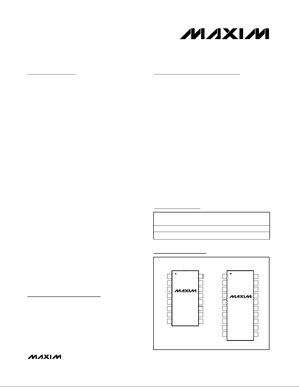
Pin Configurations
19-2084; Rev 0; 7/01
For pricing, delivery, and ordering information, please contact Maxim/Dallas Direct! at
1-888-629-4642, or visit Maxim’s website at www.maxim-ic.com.
Typical Operating Circuit appears at end of data sheet.
Ordering Information
PA RT
MAX1964TEEE
MAX1965TEEP
TEMP.
RANGE
-40°C to +85°C
-40°C to +85°C
PINPACKAGE
16 QSOP 200
20 QSOP 200
TOP VIEW
1
POK IN
COMP
2
OUT
3
MAX1964
4
FB
B2
5
FB2
6
B3
7
FB3
8
16-Pin QSOP
16
15
VL
14
BST
13
DH
12
LX
DL
11
10
GND
9
ILIM
POK
COMP
OUT
FB2
FB3
1
2
3
4
FB
5
B2
6
7
B3
8
9
B4
10
MAX1965
20-Pin QSOP
f
OSC
(kHz)
20
19
18
17
16
15
14
13
12
11
IN
VL
BST
DH
LX
DL
GND
ILIM
FB5
B5FB4
MAX1964/MAX1965
Tracking/Sequencing Triple/Quintuple
Power-Supply Controllers
2 _______________________________________________________________________________________
ABSOLUTE MAXIMUM RATINGS
Stresses beyond those listed under “Absolute Maximum Ratings” may cause permanent damage to the device. These are stress ratings only, and functional
operation of the device at these or any other conditions beyond those indicated in the operational sections of the specifications is not implied. Exposure to
absolute maximum rating conditions for extended periods may affect device reliability.
IN, B2, B3, B4 to GND............................................-0.3V to +30V
B5 to OUT...............................................................-20V to +0.3V
VL, POK, FB, FB2, FB3, FB4, FB5 to GND ...............-0.3V to +6V
LX to BST..................................................................-6V to +0.3V
BST to GND ............................................................-0.3V to +36V
DH to LX....................................................-0.3V to (V
BST
+ 0.3V)
DL, OUT, COMP, ILIM to GND......................-0.3V to (V
L
+ 0.3V)
VL Output Current ...............................................................50mA
VL Short Circuit to GND..................................................≤ 100ms
Continuous Power Dissipation (T
A
= +70°C)
16-Pin QSOP (derate 8.3mW/°C above +70°C)...........666mW
20-Pin QSOP (derate 9.1mW/°C above +70°C)...........727mW
Operating Temperature Range ...........................-40°C to +85°C
Junction Temperature......................................................+150°C
Storage Temperature Range .............................-65°C to +150°C
Lead Temperature (soldering, 10s) .................................+300°C
ELECTRICAL CHARACTERISTICS
(VIN= 12V, ILIM = FB = GND, V
BST
- VLX= 5V, TA= 0°C to +85°C. Typical values are at TA= +25°C, unless otherwise noted.)
)
Dual Mode is a trademark of Maxim Integrated Products, Inc.
PARAMETER SYMBOL CONDITIONS MIN TYP MAX UNITS
GENERAL
Operating Input Voltage Range
(Note 1)
V
IN
4.5 28 V
VFB = 0, V
Quiescent Supply Current I
VL REGULATOR
Output Voltage VL 6V < VIN < 28V, 0.1mA < I
Line Regulation VIN = 6V to 28V 3.0 %
Undervoltage Lockout Trip Level V
Minimum Bypass Capacitance C
DC-DC CONTROLLER
Output Voltage (Preset Mode) V
Typical Output Voltage Range
(Adjustable Mode) (Note 2)
FB Set Voltage (Adjustable
Mode)
FB Dual-Mode™ Threshold 50 100 150 mV
FB Input Leakage Current I
FB to COMP Transconductance g
Current-Sense Amplifier Voltage
Gain
Current-Limit Threshold
(Internal Mode)
Current-Limit Threshold
(External Mode)
Switching Frequency f
IN
UVLO
BYP(MIN
OUT
V
OUT
V
SET
FB
A
LIM
V
VALLEYVILIM
V
VALLEYVILIM
OSC
V
= V
FB2
= -0.1V
V
FB5
VL rising, 3% hysteresis (typ) 3.2 3.5 3.8 V
10mΩ < ESR < 500mΩ 1 µF
FB = GND 3.272 3.34 3.355 V
FB = COMP 1.221 1.236 1.252 V
VFB = 1.5V 0.01 100 nA
FB = COMP, I
m
VIN - VLX = 250mV 4.46 4.9 5.44 V/V
= 5.0V 190 250 310 mV
= 2.5V 440 530 620 mV
FB3
OUT
= 4V,
= V
= 1.5V,
FB4
= ±5µA 70 100 140 µS
COMP
MAX1964 1.25 2.5
MAX1965 1.5 3.0
<20mA 4.75 5.00 5.25 V
LOAD
V
SET
160 200 240 kHz
0.75 ✕ V
mA
IN
V
MAX1964/MAX1965
Tracking/Sequencing Triple/Quintuple
Power-Supply Controllers
_______________________________________________________________________________________ 3
ELECTRICAL CHARACTERISTICS
(VIN= 12V, ILIM = FB = GND, V
BST
- VLX= 5V, TA= 0°C to +85°C. Typical values are at TA= +25°C, unless otherwise noted.)
PARAMETER SYMBOL CONDITIONS MIN TYP MAX UNITS
Maximum Duty Cycle D
Soft-Start Period t
Soft-Start Step Size V
FB Power-Up Sequence
Threshold
DH Output Low Voltage I
DH Output High Voltage I
DL Output Low Voltage I
DL Output High Voltage I
DH On-Resistance High (DH to BST) and low (DH to LX) 1.5 4 Ω
DL On-Resistance
Output Drive Current Sourcing or sinking, VDH or VDL = VL/2 0.5 A
LX, BST Leakage Current V
POSITIVE ANALOG GAIN BLOCKS
FB2, FB3, FB4 Regulation
Voltage
FB2 Power-Up Sequence
Threshold
FB2, FB3, FB4 to B_
Transconductance Error
Feedback Input Leakage
Current
Driver Sink Current IB_
NEGATIVE ANALOG GAIN BLOCK
FB5 Regulation Voltage
FB5 to B5 Tr anscond uctance E r r or ∆V
Feedback Input Leakage Current I
Driver Source Current I
POWER GOOD (POK)
OUT Trip Level (Preset Mode) FB = GND, falling edge, 3% hysteresis (typ) 2.88 3.0 3.12 V
FB Trip Level (Adjustable Mode) Falling edge, 3% hysteresis (typ) 1.070 1.114 1.159 V
FB2, FB3, FB4 Trip Level Falling edge, 3% hysteresis (typ) 1.070 1.114 1.159 V
FB5 Trip Level Rising edge, 35mV hysteresis (typ) 368 530 632 mV
POK Output Low Level I
POK Output High Leakage V
MAX
SOFT
77 82 90 %
1024 1/f
/64 V
REF
MAX1964, FB rising, B2 turns on 1.145 V
= 10mA, measured from DH to LX 40 mV
SINK
= 10m A, m easur ed fr om BS T to D H 40 mV
S OU RC E
= 10mA, measured from DL to GND 20 mV
SINK
= 10m A, m easur ed fr om D L to GN D VL - 0.1 V
S OU RC E
High (DL to VL) 4.3 10
Low (DL to GND) 0.7 2
= VLX = VIN = 28V, VFB = 1.5V 0.04 10 µA
BST
VB2 = VB3 = VB4 = 5V,
= IB3 = IB4 = 1mA (sink)
I
B2
1.226 1.24 1.257 V
MAX1964, FB2 rising, B3 turns on 1.145 V
= VB3 = VB4 = 5V, IB2 = IB3 = IB4 =
V
∆V
FB
I
_V
FB
FB5
FB5
B5
B2
_
0.5mA to 5mA (sink)
= V
FB2
V
= V
FB2
V
= 1.188V
FB4
V
= V
B5
(source)
FB3
FB3
OUT
= V
= 1.5V 0.01 100 nA
FB4
VB2 = VB3 = VB4 = 2.5V 10 21
=
V
= VB3 = VB4 = 4.0V 24
B2
- 2V, V
= 3.5V, IB5 = 1mA
OUT
-20 -5 +10 mV
13 22 mV
VB5 = 0, IB5 = 0.5mA to 5mA (source) -13 -20 mV
V
= -100mV 0.01 100 nA
FB5
V
= 200mV, VB5 = V
FB5
3.5V
= 1mA 0.4 V
SINK
= 5V 1 µA
POK
OUT
- 2.0V, V
OUT
=
10 25 mA
OSC
Ω
mA
MAX1964/MAX1965
Tracking/Sequencing Triple/Quintuple
Power-Supply Controllers
4 _______________________________________________________________________________________
ELECTRICAL CHARACTERISTICS
(VIN= 12V, ILIM = FB = GND, V
BST
- VLX= 5V, TA= -40°C to +85°C, unless otherwise noted.) (Note 4)
ELECTRICAL CHARACTERISTICS (continued)
(VIN= 12V, ILIM = FB = GND, V
BST
- VLX= 5V, TA= 0°C to +85°C. Typical values are at TA= +25°C, unless otherwise noted.)
PARAMETER SYMBOL CONDITIONS MIN TYP MAX UNITS
THERMAL PROTECTION (NOTE 3)
Thermal Shutdown Rising temperature 160 °C
Thermal Shutdown Hysteresis 15 °C
PARAMETER SYMBOL CONDITIONS MIN TYP MAX UNITS
GENERAL
Operating Input Voltage Range
(Note 1)
Quiescent Supply Current I
VL REGULATOR
Output Voltage VL 6V < VIN < 28V, 0.1mA < I
Line Regulation VIN = 6V to 28V 3.0 %
Undervoltage Lockout Trip Level V
DC-DC CONTROLLER
Output Voltage (Preset Mode) V
Feedback Set Voltage
(Adjustable Mode)
Current-Sense Amplifier Voltage
Gain
Current-Limit Threshold
(Internal Mode)
Current-Limit Threshold
(External Mode)
Switching Frequency f
Maximum Duty Cycle D
POSITIVE ANALOG GAIN BLOCKS
FB2, FB3, FB4 Regulation
Voltage
FB2, FB3, FB4 to B_
Transconductance Error
V
IN
VFB = 0, V
IN
UVLO
OUT
V
SET
A
LIM
V
VALLEYVILIM
V
VALLEYVILIM
OSC
MAX
∆V
FB
V
V
VL rising, 3% hysteresis (typ) 3.0 4.0 V
FB = GND 3.247 3.38 V
FB = COMP 1.211 1.261 V
VIN - VLX = 250mV 4.12 5.68 V/V
VB2 = VB3 = VB4 = 5V,
I
V
_
0.5mA to 5mA (sink)
= 4V,
OUT
= V
= V
FB2
FB3
= -0.1V
FB5
= 5.0V 150 350 mV
= 2.5V 400 660 mV
= IB3 = IB4 = 1mA (sink)
B2
= VB3 = VB4 = 5V, IB2 = IB3 = IB4 =
B2
FB4
= 1.5V,
MAX1964 2.5
MAX1965 3.0
<20mA 4.75 5.25 V
LOAD
4.5 28 V
160 240 kHz
74 90 %
1.215 1.265 V
mA
28 mV
MAX1964/MAX1965
Tracking/Sequencing Triple/Quintuple
Power-Supply Controllers
_______________________________________________________________________________________ 5
Note 1: Connect VL to IN for operation with VIN< 5V.
Note 2: See Output Voltage Selection section.
Note 3: The internal 5V linear regulator (VL) powers the thermal shutdown block. Shorting VL to GND disables thermal shutdown.
Note 4: Specifications to -40°C are guaranteed by design, not production tested.
ELECTRICAL CHARACTERISTICS (continued)
(VIN= 12V, ILIM = FB = GND, V
BST
- VLX= 5V, TA= -40°C to +85°C, unless otherwise noted.) (Note 4)
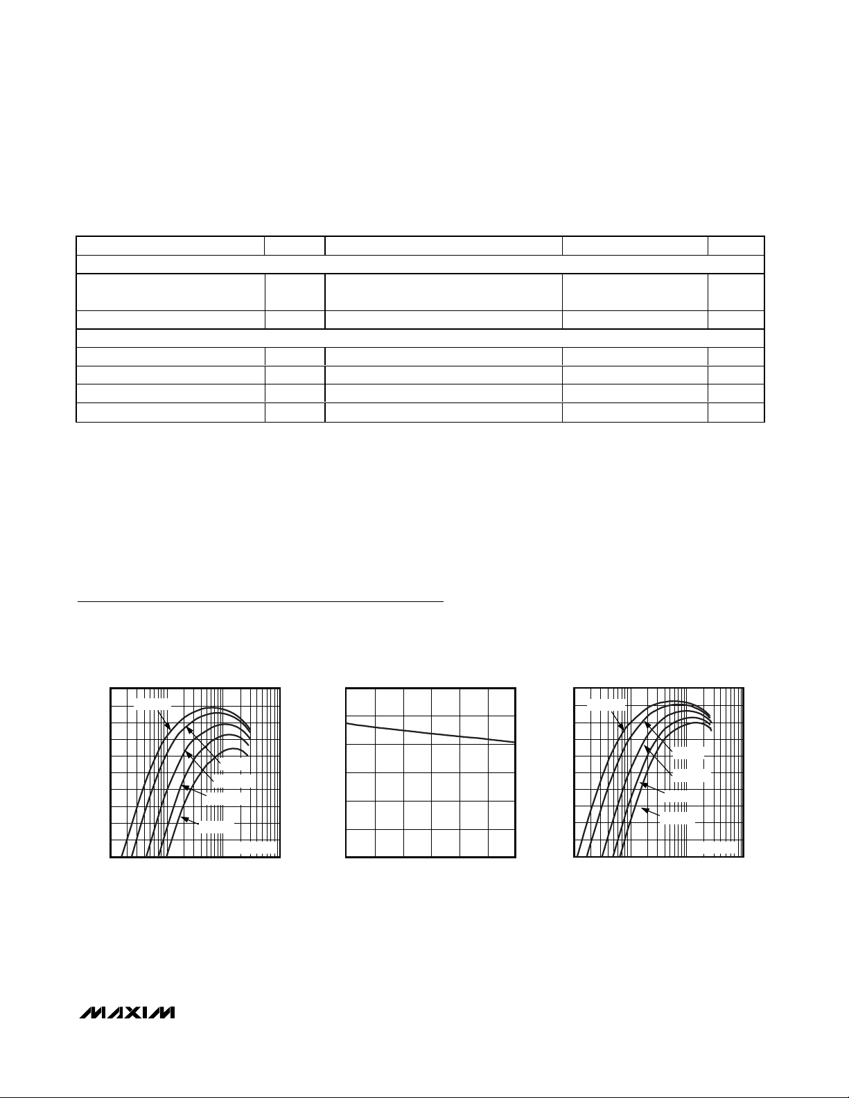
Typical Operating Characteristics
(Circuit of Figure 1, VIN= 12V, V
OUT
= 3.3V, TA= +25°C, unless otherwise noted.)
50
0.01 1010.1
EFFICIENCY vs. LOAD CURRENT
(PRESET MODE)
100
70
60
90
80
MAX1964/65 toc01
LOAD CURRENT (A)
EFFICIENCY (%)
VIN = 6.5V
VIN = 8V
VIN = 12V
VIN = 18V
VIN = 24V
V
OUT
= 3.3V
3.27
3.29
3.28
3.31
3.30
3.32
3.33
0 1.0 1.50.5 2.0 2.5 3.0
OUTPUT VOLTAGE vs. LOAD CURRENT
(PRESET MODE)
MAX1964/65 toc02
LOAD CURRENT (A)
OUTPUT VOLTAGE (V)
50
0.01 1010.1
EFFICIENCY vs. LOAD CURRENT
(ADJUSTABLE MODE)
100
70
60
90
80
MAX1964/65 toc03
LOAD CURRENT (A)
EFFICIENCY (%)
VIN = 6.5V
VIN = 8V
VIN = 12V
VIN = 18V
VIN = 24V
V
OUT
= +5.0V
PARAMETER SYMBOL CONDITIONS MIN TYP MAX UNITS
NEGATIVE ANALOG GAIN BLOCK
FB5 Regulation Voltage
FB5 to B5 Tr anscond uctance E r r or ∆V
POWER GOOD (POK)
OUT Trip Level (Preset Mode) FB = GND, falling edge, 3% hysteresis (typ) 2.85 3.15 V
FB Trip Level (Adjustable Mode) Falling edge, 3% hysteresis (typ) 1.058 1.17 V
FB2, FB3, FB4 Trip Level Falling edge, 3% hysteresis (typ) 1.058 1.17 V
FB5 Trip Level Rising edge, 35mV hysteresis (typ) 325 675 mV
V
= V
B5
= 1mA (source)
I
B5
VB5 = 0, IB5 = 0.5mA to 5mA (source) -30 mV
FB5
OUT
- 2V, V
OUT
= 3.5V,
-25 +10 mV
MAX1964/MAX1965
Tracking/Sequencing Triple/Quintuple
Power-Supply Controllers
6 _______________________________________________________________________________________
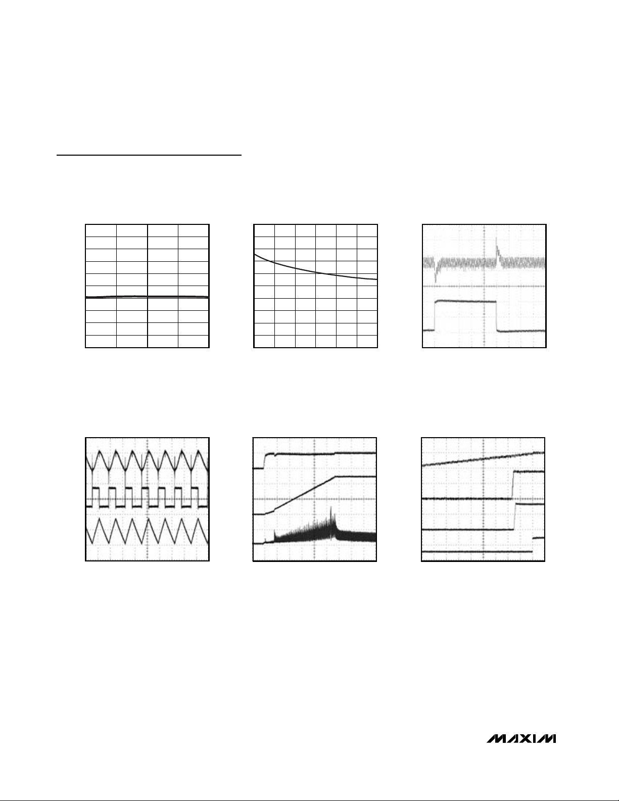
Typical Operating Characteristics (continued)
(Circuit of Figure 1, VIN= 12V, V
OUT
= 3.3V, TA= +25°C, unless otherwise noted.)
1.00.50 1.5 2.0
OUPUT VOLTAGE vs. LOAD CURRENT
(ADJUSTABLE MODE)
MAX1964/65 toc04
LOAD CURRENT (A)
OUTPUT VOLTAGE (V)
4.97
4.99
5.01
4.95
5.03
5.05
4.95
4.97
4.99
5.01
5.03
5.05
0105 15202530
INTERNAL 5V LINEAR REGULATOR
vs. LOAD CURRENT
MAX1964/65 toc05
LOAD CURRENT (mA)
VL (V)
LOAD TRANSIENT
(STEP-DOWN CONVERTER)
MAX1964/65 toc06
5.0V
0
1A
A. V
OUT
= 5V, 100mV/div
B. I
OUT
= 10mA TO 1A, 500mA/div
V
IN
= 12V
B
A
40µs/div
SWITCHING WAVEFORMS
(STEP-DOWN CONVERTER)
MAX1964/65 toc07
5.00V
A. V
OUT
= 5.0V, 50mV/div
B. V
LX
,10V/div
C. INDUCTOR CURRENT, 500mA/div
V
IN
= 12V, R
OUT1
= 5V
B
A
40µs/div
C
4.95V
12V
0
1A
0.5A
SOFT-START
(STEP-DOWN CONVERTER)
MAX1964/65 toc08
5V
A. V
L
= 5V, 5V/div
B. V
OUT1
=
5V (ADJ),2V/div
C. INDUCTOR CURRENT, 1A/div
V
IN
= STEPPED FROM 0 TO 12V, R
OUT1
= 10Ω
B
A
1ms/div
C
0
5V
0
1A
0
MAX1964 STARTUP WAVEFORM
(VOLTAGE SEQUENCING)
MAX1964/65 toc09
5V
A. V
OUT1
= 5V (ADJ), 2V/div
B. V
OUT2
=
1.8V, 1V/div
C. V
OUT3
=
3.3V, 2V/div
D. V
POK
, 5V/div
V
IN
= STEPPED FROM 0 TO 12V, R
OUT1
= 5Ω
B
A
200µs/div
C
1.8V
3.3V
D
MAX1964/MAX1965
Tracking/Sequencing Triple/Quintuple
Power-Supply Controllers
_______________________________________________________________________________________ 7
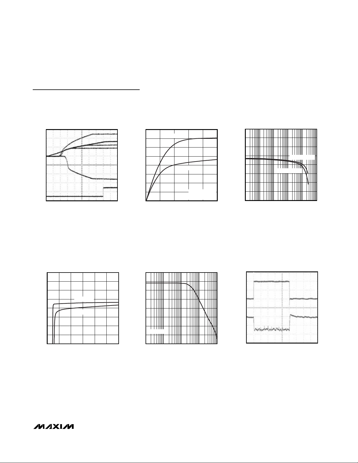
Typical Operating Characteristics (continued)
(Circuit of Figure 1, VIN= 12V, V
OUT
= 3.3V, TA= +25°C, unless otherwise noted.)
MAX1965 STARTUP WAVEFORM
(VOLTAGE TRACKING)
MAX1964/65 toc10
4V
A. V
OUT4
= 5.0V, 2V/div D. V
OUT3
=
1.8V/div
B. V
OUT1
=
3.3V, 2V/div E. V
OUT5
=
-5.0V, 2V/div
C. V
OUT2
=
2.5V, 2V/div F. V
POK
, 5V/div
V
IN
= STEPPED FROM 0 TO 12V,
R
OUT1
= 6.6Ω
CIRCUIT OF FIGURE 6
B
A
400µs/div
C
2V
0
D
E
F
-2V
-4V
5V
0
0
5
10
15
20
25
30
35
40
0246810
POSITIVE LINEAR REGULATOR BASE-
DRIVE CURRENT vs. BASE-DRIVE VOLTAGE
MAX1964/65 toc11
BASE VOLTAGE (V)
BASE-DRIVE SINK CURRENT (mA)
V
FB_
= 1.0V
V
FB_
= 0.96V
REF
B2, B3 AND B4
(MAX1965) ONLY
2.50
0.01 10.1 100
POSITIVE LINEAR REGULATOR
OUTPUT VOLTAGE vs. LOAD CURRENT
(Q
LDO
= 2N3905)
2.42
2.44
2.46
2.48
MAX1964/65 toc12
LOAD CURRENT (mA)
OUTPUT VOLTAGE (V)
10 1000
V
SUP(POS)
= 5.0V
V
SUP(POS)
= 3.3V
POSITIVE LINEAR REGULATOR
OUTPUT VOLTAGE vs. SUPPLY VOLTAGE
(Q
2.50
2.48
2.46
OUTPUT VOLTAGE (V)
2.44
LDO
I
OUT2
2.42
243 5678
SUPPLY VOLTAGE (V)
POSITIVE LINEAR REGULATOR
POWER-SUPPLY REJECTION RATIO
= 2N3905)
80
70
MAX1964/65 toc13
I
= 1mA
OUT2
= 100mA
60
50
40
PSRR (dB)
30
20
I
= 50mA
OUT2
10
0
0.1 10 10011000
= 2N3905)
(Q
LDO
FREQUENCY (kHz)
100mA
MAX1964/65 toc14
2.467V
2.457V
POSITIVE LINEAR REGULATOR
LOAD TRANSIENT
= 2N3905)
(Q
LDO
0
10µs/div
A. I
= 1mA TO 100mA, 50mA/div
OUTZ
= 2.5V, 5mV/div
B. V
OUTZ
= 10µF CERAMIC, V
C
LDO(POS)
CIRCUIT OF FIGURE 1
SUP(POS)
MAX1964/65 toc15
= 3.3V
A
B
MAX1964/MAX1965
Tracking/Sequencing Triple/Quintuple
Power-Supply Controllers
8 _______________________________________________________________________________________
Typical Operating Characteristics (continued)
(Circuit of Figure 1, VIN= 12V, V
OUT
= 3.3V, TA= +25°C, unless otherwise noted.)
2.50
0.01 0.1 1000100
POSITIVE LINEAR REGUALTOR
OUTPUT VOLTAGE vs. LOAD CURRENT
(Q
LDO
= TIP30)
2.42
2.44
2.46
2.48
MAX1964/65 toc16
LOAD CURRENT (mA)
OUTPUT VOLTAGE (V)
110
V
SUP(POS)
= 5.0V
V
SUP(POS)
= 3.3V
2.42
2.44
2.46
2.48
2.50
2 4 6 8 10 12
POSITIVE LINEAR REGULATOR
OUTPUT VOLTAGE vs. SUPPLY VOLTAGE
(Q
LDO
= TIP30)
MAX1964/65 toc17
SUPPLY VOLTAGE (V)
OUTPUT VOLTAGE (V)
I
OUT2
= 1mA
I
OUT2
= 100mA
80
70
60
50
40
30
20
10
0
0.1 10 1001 1000
POSITIVE LINEAR REGULATOR
POWER-SUPPLY REJECTION RATIO
(Q
LDO
= TIP30)
MAX1964/65 toc18
FREQUENCY (kHz)
PSRR (dB)
I
OUT2
= 150mA
POSITIVE LINEAR REGULATOR
LOAD TRANSIENT
(Q
LDO
= TIP30)
MAX1964/65 toc19
250mA
2.453V
2.473V
A. I
OUT2
= 10mA TO 250mA, 200mA/div
B. V
OUT2
= 2.5V, 10mV/div
C
LDO(POS)
= 10µF CERAMIC, V
SUP(POS)
= 3.3V
CIRCUIT OF FIGURE 1
0
B
A
10µs
0
10
5
25
20
15
40
35
30
45
0426810
NEGATIVE LINEAR REGULATOR BASE-
DRIVE CURRENT vs. BASE-DRIVE VOLTAGE
MAX1964/65 toc20
V
OUT
- VB5 (V)
BASE-DRIVE SOURCE CURRENT (mA)
V
FB5
= 250mV
V
FB5
= 50mV
V
OUT
= 5.0V
V
OUT
= 3.3V
B5 (MAX1965) ONLY
-12.00
-12.06
-12.12
-12.18
-12.24
0.01 1
10
1000.1 1000
NEGATIVE LINEAR REGULATOR
OUTPUT VOLTAGE vs. LOAD CURRENT
(Q
LDO
= TIP29)
MAX1964/65 toc21
LOAD CURRENT (mA)
OUTPUT VOLTAGE (V)
V
SUP(NEG)
= -15V
V
OUT3
= 5V
MAX1964/MAX1965
Tracking/Sequencing Triple/Quintuple
Power-Supply Controllers
_______________________________________________________________________________________ 9
Pin Description
Typical Operating Characteristics (continued)
(Circuit of Figure 1, VIN= 12V, V
OUT
- 3.3V, TA= +25°C, unless otherwise noted.)
PIN
MAX1964 MAX1965
1 1 POK
2 2 COMP
3 3 OUT
NEGATIVE LINEAR REGULATOR
OUTPUT VOLTAGE vs. SUPPLY VOLTAGE
-12.00
-12.06
-12.12
OUTPUT VOLTAGE (V)
-12.18
-12.24
-20 -18 -16 -14 -12 -10
NAME FUNCTION
Open-Drain Power-Good Output. POK is low when any output voltage is more than
10% below its regulation point. POK is high impedance when all the outputs are in
regulation. Connect a resistor between POK and VL for logic-level voltages.
Compensation Pin. Connect the compensation network to GND to compensate the
control loop.
Regulated Output Voltage High-Impedance Sense Input. Internally connected to a
resistive-divider and negative gain block (MAX1965).
= TIP29)
(Q
LDO
I
= 100mA
LDO(NEG)
I
= 1mA
LDO(NEG)
SUPPLY VOLTAGE (V)
MAX1964/65 toc22
Dual-Mode Switching-Regulator Feedback Input. Connect to GND for the preset 3.3V
44FB
55B2
6 6 FB2
output. Connect to a resistive-divider from the output to FB to GND to adjust the output
voltage between 1.236V and 0.75
Open-Drain Output PNP Transistor Driver (Regulator 2). Internally connected to the
drain of a DMOS. B2 connects to the base of an external PNP pass transistor to form a
positive linear regulator.
Analog Gain Block Feedback Input (Regulator 2). Connect to a resistive-divider
between the positive linear regulator’s output and GND to adjust the output voltage.
The feedback set point is 1.24V.
✕ V
. The feedback set point is 1.236V.
IN

MAX1964/MAX1965
Tracking/Sequencing Triple/Quintuple
Power-Supply Controllers
10 ______________________________________________________________________________________
Pin Description (continued)
PIN
MAX1964 MAX1965
77B3
8 8 FB3
— 9B4
— 10 FB4
NAME FUNCTION
Open-Drain Output PNP Transistor Driver (Regulator 3). Internally connected to the
drain of a DMOS. B3 connects to the base of an external PNP pass transistor to form a
positive linear regulator.
Analog Gain Block Feedback Input (Regulator 3). Connect to a resistive-divider
between the positive linear regulator’s output and GND to adjust the output voltage.
The feedback set point is 1.24V.
Open-Drain Output PNP Transistor Driver (Regulator 4). Internally connected to the
drain of a DMOS. B4 connects to the base of an external PNP pass transistor to form a
positive linear regulator.
Analog Gain Block Feedback Input (Regulator 4). Connect to a resistive-divider
between the positive linear regulator’s output and GND to adjust the output voltage.
The feedback set point is 1.24V.
Open-Drain Output NPN Transistor Driver (Regulator 5). Internally connected to the
— 11 B5
drain of a P-channel MOSFET. B5 connects to the base of an external NPN pass
transistor to form a negative linear regulator.
Analog Gain Block Feedback Input (Regulator 5). Connect to a resistive-divider
— 12 FB5
9 13 ILIM
10 14 GND Ground
11 15 DL Low-Side Gate-Driver Output. DL swings between GND and VL.
12 16 LX
13 17 DH High-Side Gate-Driver Output. DH swings between LX and BST.
14 18 BST
15 19 VL
16 20 IN
between the negative linear regulator’s output and a positive reference voltage,
typically one of the positive linear regulator outputs, to adjust the output voltage. The
feedback set point is at GND.
Dual-Mode Current-Limit Adjustment Input. Connect to VL for the default 250mV
current-limit threshold. In adjustable mode, the current-limit threshold voltage is 1/5 th
the voltage present at ILIM. Connect to a resistive-divider between VL and GND to
adjust V
default value is approximately VL - 1V.
Inductor Connection. Used for current-sense between IN and LX, and used for currentlimit between LX and GND.
Boost Flying Capacitor Connection. Connect BST to the external boost diode and
capacitor as shown in the Standard Application Circuit.
Internal 5V Linear Regulator Output. Supplies the IC and powers the DL low-side gate
driver and external boost diode and capacitor. Bypass with a 1µF or greater ceramic
capacitor to GND.
Input Supply Voltage. 4.5V to 28V. Bypass to GND with a 1µF or greater ceramic
capacitor close to the IC.
between 500mV and 2.5V. The logic threshold for switchover to the 250mV
ILIM

MAX1964/MAX1965
Tracking/Sequencing Triple/Quintuple
Power-Supply Controllers
______________________________________________________________________________________ 11
Detailed Description
The MAX1964/MAX1965 power-supply controllers provide system power for cable and xDSL modems. The
main step-down DC-DC controller operates in a current-mode pulse-width-modulation (PWM) control
scheme to ease compensation requirements and provide excellent load and line transient response.
The MAX1964 includes two analog gain blocks to regulate two additional positive auxiliary output voltages,
and the MAX1965 includes four analog gain blocks to
regulate three additional positive and one negative auxiliary output voltages. The positive regulator gain blocks
can be used to generate low voltage rails directly from
the main step-down converter or higher voltages using
coupled windings from the step-down converter. The
Figure 1. MAX1964 Standard Application Circuit
C
COMP1
470pF
TO LOGIC
R
COMP
5MΩ
1µF
1µF
C1
C2
100kΩ
C
COMP2
R
47pF
POK
IN
VL
ILIM
POK
COMP
D1
CENTRAL CMPSH-3
MAX1964
BST
OUT
GND
FB2
INPUT
9V TO 18V
C
IN
470µF
R
GATE(NH)
DH
LX
DL
FB
B2
10Ω
C
BST
0.1µF
R
GATE(NL)
10Ω
C
2200pF
R
BE2
220Ω
4.64kΩ
10kΩ
BE2
Q1
R3
TIP30
R4
INTERNATIONAL
RECTIFIER
N
H
IRF7101
N
L
C3
1µF
V
OUT2
1.8V AT 300mA
C4
10µF
L1
33µH
R1
30kΩ
R2
10kΩ
C
OUT
1000µF
V
OUT1
5V AT 1A
B3
FB3
: 1000µF, 10V SANYO (CZ SERIES)
OUT
C
BE3
1000pF
R
BE3
220Ω
R5
4.99kΩ
R4
3.0kΩ
Q2
TIP32
C5
1µF
V
OUT3
3.3V AT 750mA
C6
10µF
POWER GROUND
ANALOG GROUNDC

MAX1964/MAX1965
negative gain block can be used in conjunction with a
coupled winding to generate -5V, -12V, or -15V.
DC-DC Controller
The MAX1964/MAX1965 step-down converters use a
pulse-width-modulated (PWM) current-mode control
scheme (Figure 2). An internal transconductance amplifier establishes an integrated error voltage at the COMP
pin. The heart of the current-mode PWM controller is an
open-loop comparator that compares the integrated
voltage-feedback signal against the amplified currentsense signal plus the slope compensation ramp. At
each rising edge of the internal clock, the high-side
MOSFET turns on until the PWM comparator trips or the
maximum duty cycle is reached. During this on-time,
current ramps up through the inductor, sourcing current
to the output and storing energy in a magnetic field.
The current-mode feedback system regulates the peak
inductor current as a function of the output voltage error
signal. Since the average inductor current is nearly the
same as the peak inductor current (assuming that the
inductor value is relatively high to minimize ripple current), the circuit acts as a switch-mode transconductance amplifier. It pushes the output LC filter pole,
normally found in a voltage-mode PWM, to a higher frequency. To preserve inner-loop stability and eliminate
inductor stair casing, a slope-compensation ramp is
summed into the main PWM comparator.
During the second-half of the cycle, the high-side MOSFET turns off and the low-side N-Channel MOSFET
turns on. Now the inductor releases the stored energy
as its current ramps down, providing current to the output. Therefore, the output capacitor stores charge when
the inductor current exceeds the load current, and discharges when the inductor current is lower, smoothing
the voltage across the load. Under overload conditions
when the inductor current exceeds the selected current-limit (see the Current Limit section), the high-side
MOSFET is not turned on at the rising edge of the clock
and the low-side MOSFET remains on to let the inductor
current ramp down.
The MAX1964/MAX1965 operate in a forced-PWM
mode, so even under light loads, the controller maintains a constant switching frequency to minimize crossregulation errors in applications that use a transformer.
So the low-side gate-drive waveform is the complement
of the high-side gate-drive waveform, which causes the
inductor current to reverse under light loads.
Current-Sense Amplifier
The one MAX1964/MAX1965’s one current-sense circuit
amplifies (A
V
= 4.9) the current-sense voltage
generated by the high-side MOSFET’s on resistance
(R
DS(ON)
✕
I
INDUCTOR
). This amplified current-sense
signal and the internal slope compensation signal are
summed together (V
SUM
) and fed into the PWM comparator’s inverting input. The PWM comparator turns off
the high-side MOSFET when the V
SUM
exceeds the
integrated feedback voltage (V
COMP
). Place the highside MOSFET no further than 5mm from the controller
and connect IN and LX to the MOSFET using Kelvin
sense connections to guarantee current-sense accuracy and improve stability.
Current-Limit Circuit
The current-limit circuit employs a unique “valley” current-limiting algorithm that uses the low-side MOSFET’s
on-resistance as a sensing element (Figure 3). If the
voltage across the low-side MOSFET (R
DS(ON)
✕
I
INDUCTOR
) exceeds the current-limit threshold at the
beginning of a new oscillator cycle, the MAX1964/
MAX1965 will not turn on the high-side MOSFET. The
actual peak current is greater than the current-limit
threshold by an amount equal to the inductor ripple current. Therefore, the exact current-limit characteristic
and maximum load capability are a function of the lowside MOSFET on-resistance, inductor value, input voltage, and output voltage. The reward for this uncertainty
is robust, lossless overcurrent limiting.
In adjustable mode, the current-limit threshold voltage is
approximately one-fifth the voltage seen at ILIM (I
VALLEY
= 0.2 ✕V
ILIM
). Adjust the current-limit threshold by connecting a resistive-divider from VL to ILIM to GND. The
current-limit threshold can be set from 106mV to
530mV, which corresponds to ILIM input voltages of
500mV to 2.5V. This adjustable current limit accommodates MOSFETs with a wide range of on-resistance
characteristics (see the Design Procedure section). The
current-limit threshold defaults to 250mV when ILIM is
connected to VL. The logic threshold for switchover to
the 250mV default value is approximately VL - 1V.
Carefully observe the PC board layout guidelines to
ensure that noise and DC errors don’t corrupt the current-sense signals seen by LX and GND. The IC must
be mounted close to the low-side MOSFET with short
(less than 5mm), direct traces making a Kelvin sense
connection.
Synchronous Rectifier Driver (DL)
Synchronous rectification reduces conduction losses in
the rectifier by replacing the normal Schottky catch
diode with a low-resistance MOSFET switch. The
MAX1964/MAX1965 also use the synchronous rectifier
to ensure proper startup of the boost gate-driver circuit
and to provide the current-limit signal.
Tracking/Sequencing Triple/Quintuple
Power-Supply Controllers
12 ______________________________________________________________________________________

MAX1964/MAX1965
Tracking/Sequencing Triple/Quintuple
Power-Supply Controllers
______________________________________________________________________________________ 13
Figure 2a. MAX1964 Functional Diagram
COMP
OUT
BIAS
MAX1964
ENABLE
OK
THERMAL
SHDN
V
REF
1.114V
3.5V
FB2
FB3
FB
SOFTSTART
100mV
0.9V
REF
B2
0.9V
REF
V
REF
1.24V
CLK
∑
= 4.9
A
V
SLOPE
COMP
= 5
A
V
100kΩ
400kΩ
VL LDO
5V
IN
VL
BST
DH
LX
DL
GND
ILIM
B3
0.9V
0.9VL
250mV
REF
ENABLE
POK

MAX1964/MAX1965
Tracking/Sequencing Triple/Quintuple
Power-Supply Controllers
14 ______________________________________________________________________________________
Figure 2b. MAX1965 Functional Diagram
BIAS
OK
THERMAL
SHDN
COMP
OUT
MAX1965
ENABLE
V
REF
1.114V
3.5V
FB
FB_
FB5
100mV
0.9V
REF
B_
0.9V
REF
B5
OUT
SOFTSTART
V
REF
1.24V
CLK
∑
IN
= 4.9
A
V
SLOPE
COMP
= 5
A
V
250mV
100kΩ
400kΩ
VL LDO
5V
VL
BST
DH
LX
DL
GND
ILIM
0.9VL
POK
500mV
ENABLE

The DL low-side drive waveform is always the complement of the DH high-side drive waveform (with controlled dead time to prevent cross-conduction or
“shoot-through”). A dead-time circuit monitors the DL
output and prevents the high-side FET from turning on
until DL is fully off. In order for the dead-time circuit to
work properly, there must be a low-resistance, lowinductance path from the DL driver to the MOSFET
gate. Otherwise, the sense circuitry in the MAX1964/
MAX1965 will interpret the MOSFET gate as “off” when
gate charge actually remains. Use very short, wide
traces (50mils to 100mils wide if the MOSFET is 1 inch
from the device). The dead time at the other edge (DH
turning off) is determined by a fixed internal delay.
High-Side Gate-Drive Supply (BST)
Gate-drive voltage for the high-side N-channel switch is
generated by a flying-capacitor boost circuit (Figure 1).
The capacitor between BST and LX is alternately
charged from the VL supply and placed parallel to the
high-side MOSFET’s gate and source terminals.
On startup, the synchronous rectifier (low-side MOSFET) forces LX to ground and charges the boost
capacitor to 5V. On the second half-cycle, the switchmode power supply turns on the high-side MOSFET by
closing an internal switch between BST and DH. This
provides the necessary gate-to-source voltage to turn
on the high-side switch, an action that boosts the 5V
gate-drive signal above the input voltage.
Internal 5V Linear Regulator (VL)
All MAX1964/MAX1965 functions, except the currentsense amplifier, are internally powered from the onchip, low-dropout 5V regulator. The maximum regulator
input voltage (VIN) is 28V. Bypass the regulator’s output
(VL) with a ceramic capacitor of at least 1µF to GND.
The VIN-to-VL dropout voltage is typically 200mV, so
when VINis less than 5.2V, VL is typically VIN- 200mV.
The internal linear regulator can source up to 20mA to
supply the IC, power the low-side gate driver, charge
the external boost capacitor, and supply small external
loads. When driving particularly large FETs, little or no
regulator current may be available for external loads.
For example, when switched at 200kHz, a large FET
with 40nC total gate charge requires 40nC x 200kHz, or
8mA.
Undervoltage Lockout
If VL drops below 3.5V, the MAX1964/MAX1965
assumes that the supply voltage is too low to make
valid decisions, so the undervoltage lockout (UVLO)
circuitry inhibits switching, forces POK low, and forces
the DL and DH gate drivers low. After VL rises above
3.5V, the controller powers up the outputs (see Startup
section).
Startup
Externally, the MAX1964/MAX1965 start switching when
VL rises above the 3.5V undervoltage lockout threshold. However, the controller is not enabled unless all
four conditions are met: 1) VL exceeds the 3.5V undervoltage lockout threshold, 2) the internal reference
exceeds 92% of its nominal value (V
REF
> 1.145V), 3)
the internal bias circuitry powers up, and 4) the thermal
limit is not exceeded. Once the MAX1964/MAX1965
assert the internal enable signal, the step-down controller starts switching and enables soft-start.
The soft-start circuitry gradually ramps up to the reference voltage in order to control the rate of rise of the
step-down controller and reduce input surge currents
MAX1964/MAX1965
Tracking/Sequencing Triple/Quintuple
Power-Supply Controllers
______________________________________________________________________________________ 15
Figure 3. “Valley” Current-Limit Threshold Point
INDUCTOR CURRENT
-I
PEAK
I
LOAD
I
VALLEY
(VIN - V
)
V
OUT
OUT
+
[
()
L
VINƒ
OSC
]
TIME
I
PEAK
= I
VALLEY

MAX1964/MAX1965
during startup. The soft-start period is 1024 clock
cycles (1024/f
OSC
), and the internal soft-start DAC
ramps up the voltage in 64 steps. The output reaches
regulation when soft-start is completed, regardless of
output capacitance and load.
Output Voltage Sequencing (MAX1964)
After the reference powers up, the controller begins a
startup sequence. First, the main DC-DC step-down
converter powers up with soft-start enabled. Once the
step-down converter reaches 92% of its nominal value
(VFB> 1.145V) and soft-start is completed, the controller powers up the first positive linear regulator. Once
the first linear regulator reaches 92% of its nominal
value (V
FB2
> 1.145V), the second linear regulator powers up. Once all three output voltages exceed 92% of
their nominal values, the active-high ready signal (POK)
goes high (see Power-Good Output section).
Output Voltage Tracking (MAX1965)
After the reference powers up, the controller simultaneously powers up all five output voltages. The main DCDC step-down converter powers up with soft-start
enabled while the linear regulators are fully activated.
However, the linear regulators’ inputs are typically connected to or derived from the step-down converter output voltage. Since the linear regulators are fully active,
the pass transistors immediately saturate, allowing
these output voltages to track the step-down converter’s slow rising output voltage (see Typical Operating
Characteristics). Once all five output voltages exceed
92% of their nominal values, the active-high ready signal (POK) goes high (see Power-Good Output section).
Power-Good Output (POK)
POK is an open-drain output. The MOSFET turns on
and pulls POK low when any output falls below 90% of
its nominal regulation voltage. Once all of the outputs
exceed 92% of their nominal regulation voltages and
soft-start is completed, POK goes high impedance. To
obtain a logic voltage output, connect a pullup resistor
from POK to VL. A 100kΩ resistor works well for most
applications. If unused, leave POK grounded or unconnected.
Thermal overload Protection
Thermal overload protection limits total power dissipation in the MAX1964/MAX1965. When the junction temperature exceeds TJ= +160°C, a thermal sensor shuts
down the device, forcing DL and DH low, allowing the
IC to cool. The thermal sensor turns the part on again
after the junction temperature cools by 15°C, resulting
in a pulsed output during continuous thermal overload
conditions. If the VL output is short-circuited, thermal
overload protection is disabled.
During a thermal event, the main step-down converter
and the linear regulators are turned off, POK goes low,
and soft-start is reset.
Design Procedure
DC-DC Step-Down Converter
Output Voltage Selection
The step-down controller’s feedback input features dual
mode operation. Connect the output to OUT and connect FB to GND for the preset 3.3V output voltage.
Alternatively, the MAX1964/MAX1965 output voltage
may be adjusted by connecting a voltage-divider from
the output to FB to GND (Figure 4). Select R2 in the
5kΩ to 50kΩ range. Calculate R1 with the following
equation:
where V
SET
= 1.236V and V
OUT
may range from 1.236V
to approximately 0.75 ✕VIN(up to 20V). If V
OUT
> 5.5V,
connect OUT to GND (MAX1964) or to one of the positive linear regulators (MAX1965) with an output voltage
between 2V and 5V.
Inductor Value
Three key inductor parameters must be specified:
inductance value (L), peak current (I
PEAK
), and DC
resistance (RDC). The following equation includes a
constant LIR, which is the ratio of inductor peak-to-peak
AC current to DC load current. A higher LIR value
allows smaller inductance, but results in higher losses
and higher output ripple. A good compromise between
size and losses is a 30% ripple-current to load-current
ratio (LIR = 0.3). The switching frequency, input voltage, output voltage, selected LIR determine the inductor value as follows:
where fSWis 200kHz. The exact inductor value is not
critical and can be adjusted in order to make trade-offs
among size, cost, and efficiency. Lower inductor values
minimize size and cost, but they also increase the output ripple and reduce the efficiency due to higher peak
currents. On the other hand, higher inductor values
increase efficiency, but at some point resistive losses
due to extra turns of wire will exceed the benefit gained
from lower AC current levels.
Tracking/Sequencing Triple/Quintuple
Power-Supply Controllers
16 ______________________________________________________________________________________
V
RR
12 1=
L
=
VVV
VI LIR
IN SW LOAD MAX
OUT
V
SET
()
OUT IN OUT
ƒ
-
-
()

Find a low-loss inductor having the lowest possible DC
resistance that fits in the allotted dimensions. Ferrite
cores are often the best choice, although powdered
iron is inexpensive and can work well at 200kHz. The
chosen inductor’s saturation rating must exceed the
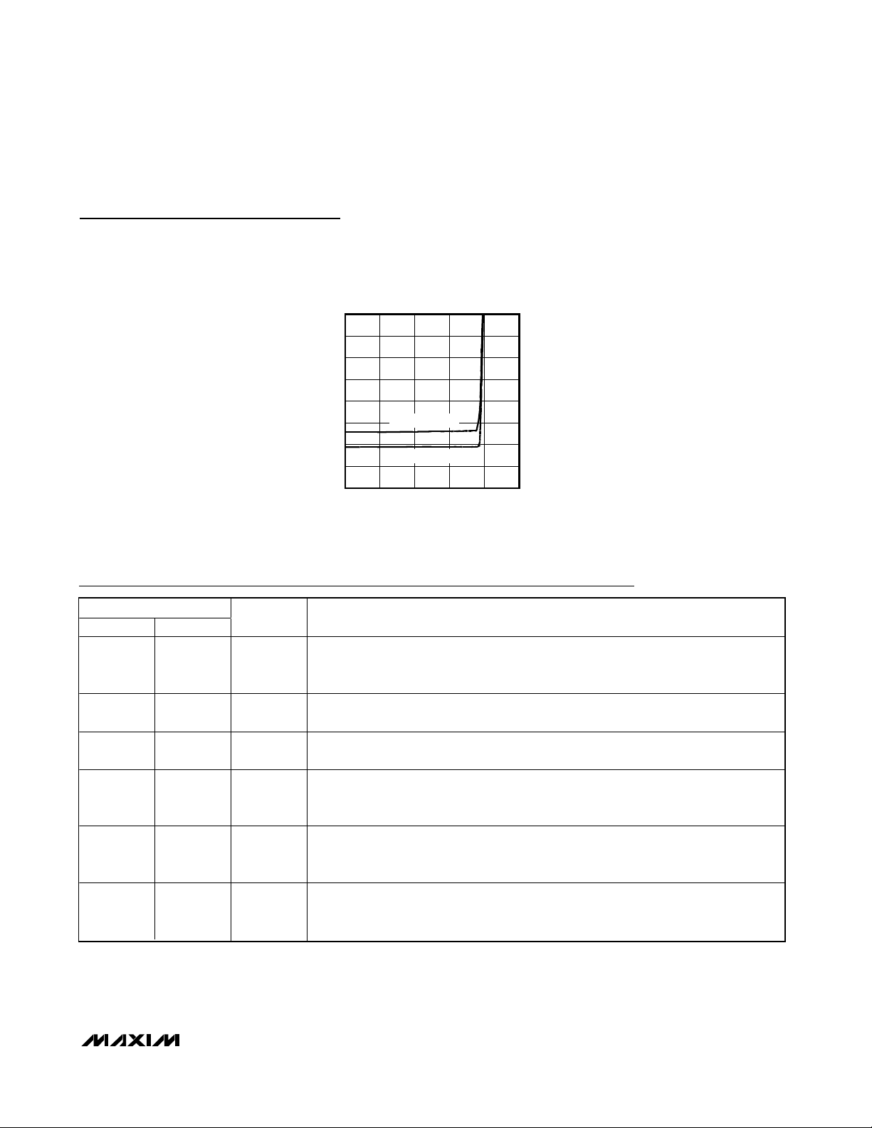
peak inductor current:
Setting the Current Limit
The minimum current-limit threshold must be high
enough to support the maximum load current at the
minimum tolerance level of the current-limit circuit. The
valley of the inductor current occurs at I
LOAD(MAX)
minus half of the ripple current:
where R
DS(ON)
is the on-resistance of the low-side
MOSFET (NL). For the MAX1964/MAX1965, the minimum current-limit threshold is 190mV (for the typical
250mV default setting). Use the worst-case maximum
value for R
DS(ON)
from the MOSFET NLdata sheet, and
add some margin for the rise in R
DS(ON)
over tempera-
ture. A good general rule is to allow 0.5% additional
resistance for each °C of the MOSFET junction temperature rise.
Connect ILIM to VL for the default 250mV (typ) currentlimit threshold. For an adjustable threshold, connect a
resistive-divider from VL to ILIM to GND. The external
adjustment range of 500mV to 2.5V corresponds to a
current-limit threshold of 106mV to 530mV. When
adjusting the current limit, use 1% tolerance resistors
and a 10µA divider current to prevent a significant
increase in the current-limit tolerance.
MOSFET Selection
The MAX1964/MAX1965’s step-down controller drives
two external logic-level N-channel MOSFETs as the circuit switch elements. The key selection parameters are:
1. On-resistance (R
DS(ON)
)
2. Maximum drain-to-source voltage (V
DS(MAX)
)
3. Minimum threshold voltage (V
TH(MIN)
)
4. Total gate charge (Q
g
)
5. Reverse transfer capacitance (C
RSS
)
The high-side N-channel MOSFET must be a logic-level
type with guaranteed on-resistance specifications at
V
GS
≤ 4.5V. Select the high-side MOSFET’s on-resis-
tance (R
DS(ON)
) so I
PEAK
✕
R
DS(ON)
≤ 225mV for the
MAX1964/MAX1965
Tracking/Sequencing Triple/Quintuple
Power-Supply Controllers
______________________________________________________________________________________ 17
Figure 4. Adjustable Output Voltage
MAX1964
IN
MAX1965
VL
ILIM
POK
COMP
C1
C2
R
POK
R
COMP
C
COMP1
* FOR OUTPUT VOLTAGES > 5V, SEE "OUTPUT VOLTAGE SELECTION."
C
COMP2
LIR
II
=+
PEAK LOAD MAX LOAD MAX
() ()
I
2
V
VALLEY LOW
R
DS ON
()
()
>−
I
LOAD MAX LOAD MAX
() ()
LIR
2
I
INPUT
D1
BST
DH
C
BST
OUT
GND
LX
DL
FB
4.5V TO 28V
C
IN
N
H
L
N
L
OUTPUT
1.25V TO 5V*
C
OUT
R1
R2

MAX1964/MAX1965
current-sense range. For a good compromise between
efficiency and cost, choose a high-side MOSFET (NH)
that has conduction losses equal to the switching losses at the optimum input voltage. Check to ensure that
the conduction losses at minimum input voltage don’t
exceed the package thermal limits or violate the overall
thermal budget. Check to ensure that the conduction
losses plus switching losses at the maximum input voltage don’t exceed package ratings or violate the overall
thermal budget.
The low-side MOSFET (NL) provides the current-limit
signal, so choose a MOSFET with an R
DS(ON)
large
enough to provide adequate circuit protection (see the
Setting the Current-Limit section):
Use the worst-case maximum value for R
DS(ON)
from
the MOSFET NL data sheet, and add some margin for
the rise in R
DS(ON)
over temperature. A good general
rule is to allow 0.5% additional resistance for each °C of
the MOSFET junction temperature rise. Ensure that the
MAX1964/MAX1965 DL gate drivers can drive NL; in
other words, check that the dv/dt caused by NHturning
on does not pull up the NLgate due to drain-to-gate
capacitance, causing cross-conduction problems.
MOSFET package power dissipation often becomes a
dominant design factor. I2R power losses are the greatest heat contributor for both high-side and low-side
MOSFETs. I2R losses are distributed between NHand
N
L
according to duty factor as shown in the equations
below. Generally, switching losses affect only the highside MOSFET, since the low-side MOSFET is a zerovoltage switched device when used in the buck
topology.
Gate-charge losses are dissipated by the driver and do
not heat the MOSFET. Calculate the temperature rise
according to package thermal-resistance specifications
to ensure that both MOSFETs are within their maximum
junction temperature at high ambient temperature. The
worst-case dissipation for the high-side MOSFET (PNH)
occurs at both extremes of input voltage, and the worstcase dissipation for the low-side MOSFET (PNL) occurs
at maximum input voltage.
I
GATE
is the average DH driver output current capability
determined by:
where R
DS(ON)DH
is the high-side MOSFET driver’s on-
resistance (4Ω max), and R
GATE
is any resistance
placed between DH and the high-side MOSFET’s gate
(Figure 5).
To reduce EMI caused by switching noise, add a 0.1µF
ceramic capacitor from the high-side switch drain to the
low-side switch source or add resistors (max 47Ω) in
series with DL and DH to increase the switches’ turn-on
and turn-off times (Figure 5).
The minimum load current should exceed the high-side
MOSFET’s maximum leakage current over temperature
if fault conditions are expected.
Input Capacitor
The input filter capacitor reduces peak currents drawn
from the power source and reduces noise and voltage
ripple on the input caused by the circuit’s switching.
The input capacitor must meet the ripple current
requirement (I
RMS
) imposed by the switching currents
defined by the following equation:
Tracking/Sequencing Triple/Quintuple
Power-Supply Controllers
18 ______________________________________________________________________________________
Figure 5. Reducing the Switching EMI
V
R
DS ON
()
=
I
VALLEY
VALLEY
QQ
+
PVI
NH SWITCHING IN LOAD OSC
()
=ƒ
GS GD
I
GATE
I
=
GATE
2
RR
()
VL
()
DS ON DH GATE
+
PIR
NH CONDUCTION LOAD DS ON NH
()()
PP P
NH TOTAL NH SWITCHING NH CONDUCTION
()( )( )
PI R
=
NL LOAD DS ON NL
2
=
=+
()
2
V
OUT
1-
V
IN
V
OUT
V
IN
MAX1964
MAX1965
TO VL
BST
GND
R
GATE
(OPTIONAL)
DH
C
LX
DH
BST
R
GATE
(OPTIONAL)
N
H
L
N
L

I
RMS
has a maximum value when the input voltage
equals twice the output voltage (VIN= 2V
OUT
), so
I
RMS(MAX)
= I
LOAD
/2. For most applications, nontantalum capacitors (ceramic, aluminum, polymer, or OSCON) are preferred due to their robustness with high
inrush currents typical of systems with low impedance
inputs. Additionally, two (or more) smaller value lowESR capacitors can be connected in parallel for lower
cost. Choose an input capacitor that exhibits less than
+10°C temperature rise at the RMS input current for
optimal circuit long-term reliability.
Output Capacitor
The key selection parameters for the output capacitor
are the actual capacitance value, the equivalent series
resistance (ESR), and voltage-rating requirements
which affect the overall stability, output ripple voltage,
and transient response.
The output ripple has two components: variations in the
charge stored in the output capacitor, and the voltage
drop across the capacitor’s equivalent series resistance (ESR) caused by the current into and out of the
capacitor.
V
RIPPLE =VRIPPLE(ESR) + VRIPPLE(C)
The output voltage ripple as a consequence of the ESR
and output capacitance is:
where I
p-p
is the peak-to-peak inductor current (see
Inductor Selection section). These equations are suitable for initial capacitor selection, but final values
should be set by testing a prototype or evaluation circuit. As a general rule, a smaller ripple current results in
less output ripple. Since the inductor ripple current is a
factor of the inductor value and input voltage, the output voltage ripple decreases with larger inductance,
but increases with lower input voltages.
With low-cost aluminum electrolytic capacitors, the
ESR-induced ripple can be larger than that caused by
the charge into and out of the capacitor. Consequently,
high quality low-ESR aluminum-electrolytic, tantalum,
polymer, or ceramic filter capacitors are required to
minimize output ripple. Best results at reasonable cost
are typically achieved with an aluminum-electrolytic
capacitor in the 470µF range, in parallel with a 0.1µF
ceramic capacitor.
Since the MAX1964/MAX1965 use a current-mode control scheme, the output capacitor forms a pole that
affects circuit stability (see Compensation Design).
Furthermore, the output capacitor’s ESR also forms a
zero.
The MAX1964/MAX1965’s response to a load transient
depends on the selected output capacitor. After a load
transient, the output instantly changes by ESR x
∆I
LOAD
. Before the controller can respond, the output
will sag further depending on the inductor and output
capacitor values. After a short period of time (see
Typical Operating Characteristics), the controller
responds by regulating the output voltage back to its
nominal state. For applications that have strict transient
requirements, low-ESR high-capacitance electrolytic
capacitors are recommended to minimize the transient
voltage swing.
Do not exceed the capacitor’s voltage or ripple-current
ratings.
Compensation Design
The MAX1964/MAX1965 controllers use an internal
transconductance error amplifier whose output allows
compensation of the control loop. Connect a series
resistor and capacitor between COMP and GND to
form a pole-zero pair, and connect a second parallel
capacitor between COMP and GND to form another
pole. The external inductor, high-side MOSFET, output
capacitor, compensation resistor, and compensation
capacitors determine the loop stability. The inductor
and output capacitor are chosen based on performance, size, and cost, while the compensation resistor
and capacitors are selected to optimize control-loop
stability. The component values shown in the Standard
Application Circuit (Figures 1 and 6) yield stable operation over a broad range of input-to-output voltages.
The controller uses a current-mode control scheme that
regulates the output voltage by forcing the required
current through the external inductor, so the
MAX1964/MAX1965 use the voltage across the highside MOSFET’s on-resistance (R
DS(ON)
) to sense the
inductor current. Using the current-sense amplifier’s
output signal and the amplified feedback voltage, the
control loop determines the peak inductor current by:
MAX1964/MAX1965
Tracking/Sequencing Triple/Quintuple
Power-Supply Controllers
______________________________________________________________________________________ 19
VVV
II
=
RMS LOAD
V I ESR
RIPPLE ESR P P
V
RIPPLE C
=
I
PP
-
OUT IN OUT
=
()
=
()
8
-
VVLV
IN OUTSWOUT
ƒ
−
()
V
IN
-
I
PP
-
ƒ
C
OUT SW
V
IN

MAX1964/MAX1965
where V
REF
= 1.24V, A
VCS
is the current-sense amplifi-
er’s gain (4.9 typ), A
VEA
is the DC gain of the transconductance error amplifier (2000 typ) set by its DC output
resistance, and V
OUT(NOMINAL)
is the output voltage
set by the feedback resistive-divider (internal or external). Since the output voltage is a function of the load
current and load resistance, the total DC loop gain
(A
V(DC)
) is approximately:
The first compensation capacitor (C
COMP1
) creates the
dominant pole. Due to the current-mode control
scheme, the output capacitor also creates a pole in the
system which is a function of the load resistance. As
the load resistance increases, the frequency of the output capacitor’s pole decreases. However, the DC loop
gain increases with larger load resistance, so the unitygain bandwidth remains fixed. Additionally, the compensation resistor and the output capacitor’s ESR both
generate zeros which must be canceled out by corresponding poles. Therefore, in order to achieve stable
operation, use the following procedure to properly compensate the system:
1) The crossover frequency (the frequency at which
unity gain occurs) must be less than 1/5th the
switching frequency:
2) Determine the series compensation capacitor
(C
COMP1
) required to set the desired crossover fre-
quency:
where the error amplifier’s transconductance (g
m
)
is 100µS (see Electrical Characteristics) and A
V(DC)
is the total DC loop gain defined above.
3) Before crossover occurs, the output capacitor and
the load resistor generate a second pole:
4) The series compensation resistor and capacitor
provide a zero which can be used to cancel the
second pole in order to ensure stability:
5) For most applications using electrolytic capacitors,
the output capacitor’s ESR forms a second zero
that occurs before crossover. Applications using
low-ESR capacitors (e.g., polymer, OS-CON) may
have ESR zeros that occur after crossover.
Therefore, verify the frequency of the output capacitor’s ESR zero:
6) Finally, if the output capacitor’s ESR zero occurs
before crossover, add the parallel compensation
capacitor (C
COMP2
) to form a third pole to cancel
this second zero:
For example, the MAX1964 Standard Application
Circuit shown in Figure 1 requires a 5V output that supports up to 2A. Using the above compensation guidelines, we can determine the proper component values:
• First, select the crossover frequency to be 1/5th the
200kHz switching frequency.
• Next, determine the total DC loop gain (A
V(DC)
) so
you can calculate the series compensation capacitance (C
COMP1
). Since the applications circuit uses
the International Rectifier IRF7101 with an R
DS(ON)
of 100mΩ, the DC loop gain approximately equals
2480 and C
COMP1
must be approximately 490pF.
Select the closest standard capacitor value of
470pF.
• Determine the location of the output pole
(f
POLE(OUT)
). With a 5V output supplying 2A and a
1000µF electrolytic capacitor, the output pole
occurs at 64Hz.
Tracking/Sequencing Triple/Quintuple
Power-Supply Controllers
20 ______________________________________________________________________________________
VVA
I
=
PEAK
VRA
OUT REF VEA
OUT NOMINAL DS ON VCS
()()
A
≈≈
VDC
()
I
≈
I
PEAK
LOAD
×400
VR
OUT NOMINAL DS ON
()()
VR A
REF LOAD VEA
VRA
OUT NOMINAL DS ON VCS
()()
VR
REF LOAD
f
SW
f
≤
C
5
C
COMP
1
≥
1
2 2000
π
mVDC
()
f
C
gA
f
POLE OUT
()
==
1
CR
22ππ
OUT LOAD
I
LOAD MAX
CV
OUT OUT
R
COMP
≥
Cf
π
2
1
COMP POLE OUT
1
()
f
ZERO ESR
()
≈
1
CR
2π
OUT ESR
C
COMP
C
COMP
≈
2
RC f
21
π
()
COMP COMP ZERO ESR
Cf
COMP POLE OUT
≈
ff
()
ZERO ESR POLE OUT
1
-
() ( )
1
1
()
()
-
()

• With the output pole’s frequency and series compensation capacitor values, the required series
resistance can be determined. Based on the above
equation, select R
COMP
= 5.1MΩ.
• Now we must determine if the selected output
capacitor’s ESR generates a second zero before
crossover—the circuit shown in Figure 1 uses a
1000µF 10V Sanyo CZ-series electrolytic capacitor
with an ESR rating of 0.2Ω, so the zero occurs at
800Hz. Since crossover occurs at 40kHz, add the
second parallel compensation capacitor.
• Finally, the second compensation capacitor value
must be approximately 43pF. Select the closest
standard capacitor value of 47pF.
Boost-Supply Diode
A signal diode, such as the 1N4148, works well in most
applications. If the input voltage goes below 6V, use a
small 20mA Schottky diode for slightly improved efficiency and dropout characteristics. Do not use large
power diodes, such as the 1N5817 or 1N4001, since
high junction capacitance can charge up VL to excessive voltages.
Linear Regulator Controllers
Positive Output Voltage Selection
The MAX1964/MAX1965’s positive linear regulator output voltages are set by connecting a voltage divider
from the output to FB_ to GND (Figure 6). Select R4 in
the 1kΩ to 50kΩ range. Calculate R3 with the following
equation:
where VFB= 1.24V and V
OUT
may range from 1.24V to
30V.
Negative Output Voltage Selection (MAX1965)
The MAX1965’s negative output voltage is set by connecting a voltage divider from the output to FB5 to a
positive voltage reference (Figure 6). Select R6 in the
1kΩ to 50kΩ range. Calculate R5 with the following
equation:
where V
REF
is the positive reference voltage used and
V
OUT
may be set between 0 and -20V.
If the negative regulator is used, the OUT pin must be
connected to a voltage supply between 2V and 5V that
can source at least 25mA. Typically, the OUT pin is
connected to the step-down converter’s output.
However, if the step-down converter’s output voltage is
set higher than 5V, OUT must be connected to one of
the positive linear regulators with an output voltage
between 2V and 5V.
Transistor Selection
The pass transistors must meet specifications for current gain (h
FE
), input capacitance, collector-emitter saturation voltage, and power dissipation. The transistor’s
current gain limits the guaranteed maximum output current to:
where I
DRV
is the minimum 10mA base drive current
and RBE(220Ω) is the pullup resistor connected
between the transistor’s base and emitter. Furthermore,
the transistor’s current gain increases the linear regulator’s DC loop gain (see Stability Requirements), so
excessive gain will destabilize the output. Therefore,
transistors with current gain over 100 at the maximum
output current, such as Darlington transistors, are not
recommended. The transistor’s input capacitance and
input resistance also create a second pole, which
could be low enough to destabilize the output when
heavily loaded.
The transistor’s saturation voltage at the maximum output current determines the minimum input-to-output
voltage differential that the linear regulator will support.
Alternatively, the package’s power dissipation could
limit the useable maximum input-to-output voltage differential. The maximum power dissipation capability of
the transistor’s package and mounting must exceed the
actual power dissipation in the device. The power dissipated equals the maximum load current times the maximum input-to-output voltage differential:
P = I
LOAD(MAX)(VLDOIN - VOUT
) = I
LOAD(MAX) VCE
Stability Requirements
The MAX1964/MAX1965 linear regulators use an internal transconductance amplifier to drive an external
pass transistor. The transconductance amplifier, pass
transistor’s specifications, the base-emitter resistor,
and the output capacitor determine the loop stability. If
the output capacitor and pass transistor are not properly selected, the linear regulator will be unstable.
The transconductance amplifier regulates the output
voltage by controlling the pass transistor’s base current. Since the output voltage is a function of the load
MAX1964/MAX1965
Tracking/Sequencing Triple/Quintuple
Power-Supply Controllers
______________________________________________________________________________________ 21
V
56=
OUT
V
V
V
RR
34 1=
RR
-
FB
OUT
REF
II
LOAD MAX DRV
=
-
V
BE
h
R
FE MIN() ()
BE

MAX1964/MAX1965
Tracking/Sequencing Triple/Quintuple
Power-Supply Controllers
22 ______________________________________________________________________________________
Figure 6. MAX1965 Application Circuit
INPUT
D1
CENTRAL CMPSH-3
470µF
9V TO 18V
C
IN
POK
R7
15kΩ
IN
VL
ILIM
POK
FB
COMP
B5
FB5
C1
1µF
C2
1µF
R
100kΩ
TO LOGIC
C
COMP1
1500pF
D3
NIHON
EC10QS10
2200pF
Q4
TIP29
V
OUT5
-5V AT 50mA
R
COMP
412kΩ
C
COMP2
68pF
T1
N
= 2
S(NEG)
C10
47µF
C11
1µF
C
BE5
C5
10µF
R8
30kΩ
R
BE5
220Ω
MAX1965
CONNECT
TO V
OUT2
BST
OUT
GND
FB2
FB3
FB3
R
GATE(NH)
DH
LX
DL
B2
B3
B3
10Ω
C
BST
0.1µF
R
GATE(NL)
10Ω
C
BE2
2200pF
R
BE2
220Ω
R1
10kΩ
R2
10kΩ
C
BE3
2200pF
R
BE3
220Ω
R3
1.3kΩ
R4
3.0kΩ
C
BE4
4700pF
R
BE4
220Ω
R5
30kΩ
R6
10kΩ
N
N
Q1
TIP30
Q2
TIP32
Q3
2N3905
H
L
FAIRCHILD
FDS6912A
T1
NP = 1
C3
1µF
V
OUT2
2.5V AT 200mA
C4
10µF
C5
1µF
V
OUT3
1.8V AT 500mA
C6
10µF
C7
1µF
V
OUT3
5V AT 100mA
C9
10µF
V
OUT1
3.3V AT 1.4A
C
OUT
470µF
10V SANYO
(MV-AX SERIES)
N
= 1
S(POS)
D2
NIHON
EP05Q03L
C8
47µF
POWER GROUND
ANALOG GROUND
NOTE: ALL T1 TRANSFORMER
WINDINGS ARE ON THE SAME CORE
T1
current and load resistance, the total DC loop gain
(A
V(LDO)
) is approximately:
where VTis 26mV, and I
BIAS
is the current through the
base-to-emitter resistor (RBE). This bias resistor is typically 220Ω, providing approximately 3.2mA of bias current.
The output capacitor creates the dominant pole.
However, the pass transistor’s input capacitance creates
a second pole in the system. Additionally, the output
capacitor’s ESR generate a zero, which may be used to
cancel the second pole if necessary. Therefore, in order
to achieve stable operation, use the following equations
to verify that the linear regulator is properly compensated:
1) First, determine the dominant pole set by the linear
regulator’s output capacitor and the load resistor:
unity-gain crossover = A
V(LDO) ƒPOLE(CLDO)
2) Next, determine the second pole set by the base-toemitter capacitance (including the transistor’s input
capacitance), the transistor’s input resistance, and
the base-to-emitter pullup resistor:
3) A third pole is set by the linear regulator’s feedback
resistance and the capacitance between FB_ and
GND (including 20pF stray capacitance).
4) If the second and third pole occur well after unitygain crossover, the linear regulator will remain stable:
ƒ
POLE(FB)
and ƒ
POLE(CBE) >
2
ƒ
POLE(CLDO) AV(LDO)
However, if the ESR zero occurs before unity-gain
crossover, cancel the zero with f
POLE(FB)
by changing
circuit components such that:
Do not use output capacitors with more than 200mΩ of
ESR. Typically, more output capacitance provides the
best solution, since this also reduces the output voltage
drop immediately after a load transient.
Linear Regulator Output Capacitors
Connect at least 1µF capacitor between the linear regulator’s output and ground, as close to the MAX1964/
MAX1965 and external pass transistors as possible.
Depending on the selected pass transistor, larger
capacitor values may be required for stability (see
Stability Requirements). Furthermore, the output capacitor’s equivalent series resistance (ESR) affects stability,
providing a zero that may be necessary to cancel the
second pole. Use output capacitors with an ESR less
than 200mΩ to ensure stability and optimum transient
response.
Once the minimum capacitor value for stability is determined, verify that the linear regulator’s output does not
contain excessive noise. Although adequate for stability, small capacitor values may provide too much bandwidth, making the linear regulator sensitive to noise.
Larger capacitor values reduce the bandwidth, thereby
reducing the regulator’s noise sensitivity.
For the negative linear regulator, if noise on the ground
reference causes the design to be marginally stable,
bypass the negative output back to its reference voltage (V
REF
, Figure 7). This technique reduces the differ-
ential noise on the output.
Base-Drive Noise Reduction
The high-impedance base driver is susceptible to system noise, especially when the linear regulator is lightly
loaded. Capacitively coupled switching noise or inductively coupled EMI onto the base drive causes fluctuations in the base current, which appear as noise on the
linear regulator’s output. Keep the base-drive traces
away from the step-down converter and as short as
possible to minimize noise coupling. Resistors in series
with the gate drivers (DH and DL) reduce the LX
switching noise generated by the step-down converter
(Figure 5). Additionally, a bypass capacitor may be
placed across the base-to-emitter resistor (Figure 7).
This bypass capacitor, in addition to the transistor’s
input capacitance, could bring in a second pole that
will destabilize the linear regulator (see Stability
Requirements). Therefore, the stability requirements
determine the maximum base-to-emitter capacitance:
MAX1964/MAX1965
Tracking/Sequencing Triple/Quintuple
Power-Supply Controllers
______________________________________________________________________________________ 23
.
55
A
ƒ= =
POLE CLDO
()
ƒ=
POLE CBE
≈
V LDO
V
T
CR
22ππ
()
=
ƒ=
POLE FB
()
Ih
BIAS FE
+
1
I
LOAD
1
LDO LOAD
CRR
22π
BE BE IN BJT
()
RI Vh
BE LOAD T FE
CRVh
π
BE BE T FE
1
212π
CRR
FB
V
REF()
I
LOAD MAX
()
CV
LDO LDO
1
()
+
()
ƒ≈
POLE FB
()
1
CR
π
OUT ESR

MAX1964/MAX1965
where C
IN(Q)
is the transistor’s input capacitance, and
f
POLE(CBE)
is the second pole required for stability.
Transformer Selection
In systems where the step-down controller’s output is
not the highest voltage, a transformer may be used to
provide additional post-regulated, high-voltage outputs.
The transformer generates unregulated, high-voltage
supplies which power the positive and negative linear
regulators. These unregulated supply voltages are
dependent on the transformer’s turns ratio – number of
secondary turns (NS) divided by the number of primary
turns (NP). So the transformer must be selected to provide supply voltages high enough to keep the pass
transistors from saturating. For positive output voltages,
connect the transformer as shown in Figure 6 where the
minimum turns ratio (N
POS
= N
S(POS)/NP
) is determined
by:
where V
SAT
is the pass transistor’s saturation voltage
under full load. For negative output voltages (MAX1965
only), connect the transformer as shown in Figure 6
where the minimum turns ratio (N
NEG
= N
S(NEG)/NP
) is
determined by:
Since power transfer occurs when the low-side MOSFET is on (DL = high), the transformer cannot support
heavy loads with high duty cycles.
Snubber Design
The MAX1964/MAX1965 use current-mode control
schemes that sense the current across the high-side
MOSFET (NH). Immediately after the high-side MOSFET
turns on, the MAX1964/MAX1965 use a 60ns currentsense blanking period to minimize noise sensitivity.
However, when the MOSFET turns on, the transformer’s
secondary inductance and the diode’s parasitic capacitance form a resonant circuit that causes ringing.
Reflected back through the transformer to the primary
side, these oscillations appear across the high-side
MOSFET may last longer than the blanking period. As
Tracking/Sequencing Triple/Quintuple
Power-Supply Controllers
24 ______________________________________________________________________________________
Figure 7. Base-Drive Noise Reduction
V
SUP
C
PASS
BYP
V
POS
MAX1964
MAX1965
a) POSITIVE OUTPUT VOLTAGE
B_
FB_
C
BE
R1
R2
R
BE
Q
C
LDO
C
BE
≤
1
2π
ƒ
POLE CBE
RI Vh
BE LOAD T FE
()
RVh
BE T FE
MAX1965
b) NEGATIVE OUTPUT VOLTAGE (MAX1965 ONLY)
+
-
N
POS
VVV
LDO POS SAT DIODE
≥
++
()
V
OUT
-1
C
IN Q
()
BF5
R4
R3
B5
C
BE
V
REF
V
NEG
C
Q
PASS
R
BE
NEG
V
SUP
C
BYP
N
NEG
VVV
LDO NEG SAT DIODE
≥
++
()
V
OUT

shown in Figure 8, a series RC snubber circuit at the
diode increases the damping factor, allowing the ringing to settle quickly. Applications with multiple transformer windings require only one snubber circuit on the
highest output voltage.
The diode’s parasitic capacitance can be estimated
using the diode’s reverse voltage rating (V
RRM
), current
capability (IO), and recovery time (tRR). A rough
approximation is:
For the EC10QS10 Nihon diode used in Figure 8, the
capacitance is roughly 15pF. The output snubber only
needs to dampen the ringing, so the initial turn-on spike
that occurs during the blanking period is still present. A
100pF capacitor works well in most applications.
Larger capacitance values require more charge, thereby increasing the power dissipation.
The snubber’s time constant (t
SNUB
) must be smaller
than the 60ns blanking time. A typical RC time constant
of approximately 30ns was chosen for Figure 8:
Minimum Load Requirements (Linear Regulators)
Under no-load conditions, leakage currents from the
pass transistors supply the output capacitor, even
when the transistor is off. Generally, this is not a problem since the feedback resistors’ current drain the
excess charge. However, charge may build up on the
output capacitor over temperature, making V
LDO
rise
above its set point. Care must be taken to ensure that
the feedback resistors’ current exceeds the pass transistor’s leakage current over the entire temperature
range.
Applications Information
PC Board Layout Guidelines
Careful PC board layout is critical to achieve low
switching losses and clean, stable operation. The
switching power stage requires particular attention.
Follow these guidelines for good PC board layout:
1) Place the power components first, with ground ter-
minals adjacent (NL source, CIN, C
OUT
). If possible, make all these connections on the top layer
with wide, copper-filled areas. Keep these high-current paths short, especially at ground terminals.
2) Mount the MAX1964/MAX1965 adjacent to the
switching MOSFETs in order to keep IN-LX currentsense lines, LX-GND current-limit sense lines, and
the driver lines (DL and DH) short and wide. The
current-sense amplifier inputs are connected
between IN and LX, so these pins must be connected as close as possible to the high-side MOSFET.
The current-limit comparator inputs are connected
between LX and GND, but accuracy is not as
important, so give priority to the high-side MOSFET
connections. The IN, LX, and GND connections to
the MOSFETs must be made using Kelvin sense
connections to guarantee current-sense and current-limit accuracy.
3) Group the gate-drive components (BST diode and
capacitor, IN bypass capacitor) together near the
MAX1964/MAX1965.
4) All analog grounding must be done to a separate
solid copper ground plane, which connects to the
MAX1964/MAX1965 at the GND pin. This includes
the VL bypass capacitor, feedback resistors, compensation components (R
COMP
, C
COMP
), and
adjustable current-limit threshold resistors connected to ILIM.
5) Ensure all feedback connections are short and
direct. Place the feedback resistors as close to the
MAX1964/MAX1965 as possible.
6) When trade-offs in trace lengths must be made, it’s
preferable to allow the inductor charging path to be
made longer than the discharge path. For example,
it is better to allow some extra distance between the
input capacitors and the high-side MOSFET than to
allow distance between the inductor and low-side
MOSFET.
7) Route high-speed switching nodes away from sensitive analog areas (B_, FB_, COMP, ILIM).
Regulating High Voltage
The linear regulator controllers can be configured to
regulate high output voltages by adding a cascode
transistor to buffer the base-drive output. For example,
to generate an output voltage between 30V and 60V,
add a 2N5550 high-voltage NPN transistor as shown in
Figure 9A where VBIAS is a DC voltage between 3V
and 20V that can source at least 1mA. R
DROP
protects
the cascode transistor by decreasing the voltage
across the transistor when the pass transistor saturates.
Similarly, to regulate a negative output voltage between
-20V and -120V, add a 2N5401 high-voltage PNP transistor as shown in Figure 9B.
MAX1964/MAX1965
Tracking/Sequencing Triple/Quintuple
Power-Supply Controllers
______________________________________________________________________________________ 25
It
×
RR
C
DIODE
R
==
SNUB
0
=
V
RRM
t
SNUB
C
SNUB SNUB
30
C
ns

MAX1964/MAX1965
Output Filtering for Analog Circuits
Some applications need to generate analog and power
outputs at the same voltage. By adding an LC filter to
filter the noise present on an analog output (Figure 10),
one output voltage can provide both analog and power
outputs. The LC filter provides approximately
40dB/decade of attenuation. Select the LC corner frequency (1/2 π√LC) to provide desired attenuation. For
stable operation, the filter inductor (L
FILTER
) and output
filter capacitor (C
FILTER
) used to generate the filter
must be selected to provide an overdamped response
to output transients:
Tracking/Sequencing Triple/Quintuple
Power-Supply Controllers
26 ______________________________________________________________________________________
Figure 8. MAX1964 High-Voltage Application Requires Snubber Circuit
INPUT
D1
CENTRAL CMPSH-3
470µF
9V TO 18V
C
IN
C1
1µF
C2
1µF
TO LOGIC
R
POK
100kΩ
IN
VL
ILIM
MAX1964
POK
R
COMP
200kΩ
C
8.2nF
COMP
COMP
BST
OUT
GND
FB2
FB3
R
GATE(NH)
DH
LX
DL
FB
B2
B3
10Ω
C
BST
0.1µF
R
GATE(NL)
10Ω
10nF
470Ω
4700pF
C9
R7
C
BE2
R
BE2
220Ω
R3
30kΩ
R4
10kΩ
N
H
N
L
Q1
2N3905
C
BE3
2200pF
R
BE3
220Ω
R5
86.6kΩ
R6
10kΩ
FAIRCHILD
FDS6912A
T1
1
C3
10µF
V
OUT2
5V AT 100mA
C5
10µF
Q2
TIP30
C
OUT
470µF
D2
NIHON
EP05Q03L
C
OUT
470µF
C6
10µF
V
OUT3
12V AT 100mA
C8
10µF
V
OUT1
3.3V AT 1A
1
T1
NIHON
EC10QS10
C7
470µF
C
D3
R
SNUB
300Ω
SNUB
100pF
2
T1
POWER GROUND
ANALOG GROUND
RRC
()
DCR ESR FILTER
L
FILTER
2
+
4
≥
1

where the R
DCR
is the inductor’s DC resistance and
R
ESR
is the output filter capacitor’s effective series
resistance (ESR). Inductors with high DC resistance will
provide poor load regulation but allow the use of smaller filter capacitors:
V
OUT(FILTER)
= V
OUT(NOMINAL)
- R
DCRIOUT
Therefore, power chokes are ideal for these applications due to their high inductance values, high saturation current ratings, and low resistance.
Chip Information
TRANSISTOR COUNT: 1617
PROCESS: BiCMOS
MAX1964/MAX1965
Tracking/Sequencing Triple/Quintuple
Power-Supply Controllers
______________________________________________________________________________________ 27
Figure 9. High-Voltage Linear Regulation
V
BIAS
C
DROP
MAX1964
MAX1965
a) POSITIVE OUTPUT VOLTAGE WITH CASCODED BASE DRIVE
MAX1965
b) NEGATIVE OUTPUT VOLTAGE (MAX1965 ONLY)
WITH CASCODED BASE DRIVE
FB_
FB5
B_
Q
CASCODE
R1
R2
R4
R3
Q
CASCODE
B5
C
R
DROP
R
DROP
DROP
V
REF
V
SUP
C
Q
PASS
PASS
BYP
V
POS
V
NEG
C
NEG
V
SUP
C
BYP
R
BE
C
POS
Q
R
BE

MAX1964/MAX1965
Tracking/Sequencing Triple/Quintuple
Power-Supply Controllers
28 ______________________________________________________________________________________
Figure 10. Filtered Output for Analog Circuits
Table 1. Component Suppliers
INPUT
C
9V TO 18V
IN
D1
IN
C1
VL
C2
R
TO LOGIC
R
COMP
C
COMP1 C
COMP2
ILIM
POK
POK
COMP
MAX1964
MAX1965
BST
DH
OUT
GND
N
H
C
LX
DL
FB
BST
N
L
L
POWER GROUND
ANALOG GROUND
POWER
OUTPUT
C
OUT
L
FILTER
ANALOG
OUTPUT
C
FILTER
SUPPLIER PHONE FAX WEBSITE
INDUCTORS & TRANSFORMERS
Coilcraft 847-639-6400 847-639-1469 www.coilcraft.com
Coiltronics 561-241-7876 561-241-9339 www.coiltronics.com
ICE Components 800-729-2099 800-729-2099 www.icecomponents.com
Sumida USA 847-956-0666 847-956-0702 www.sumida.com
Toko 847-297-0070 847-699-1194 www.tokoam.com
CAPACITORS
AVX 803-946-0690 803-626-3123 www.avxcorp.com
Kemet 408-986-0424 408-986-1442 www.kemet.com
Panasonic 847-468-5624 847-468-5815 www.panasonic.com
Sanyo 619-661-6835 619-661-1055 www.secc.co.jp
Taiyo Yuden 408-573-4150 408-573-4159 www.t-yuden.com
DIODES
Central Semiconductor 516-435-1110 516-435-1824 www.centralsemi.com
International Rectifier 310-322-3331 310-322-3332 www.irf.com
Nihon 847-843-7500 847-843-2798 www.niec.co.jp
On Semiconductor 602-303-5454 602-994-6430 www.onsemi.com
Zetex 516-543-7100 516-864-7630 www.zetex.com

MAX1964/MAX1965
Tracking/Sequencing Triple/Quintuple
Power-Supply Controllers
______________________________________________________________________________________ 29
Typical Operating Circuit
IN
VL
ILIM
POK
COMP
MAX1964
MAX1965
BST
OUT
GND
FB2
INPUT
DH
LX
DL
FB
B2
OUT #2
MAIN
OUTPUT

Package Information
MAX1964/MAX1965
Tracking/Sequencing Triple/Quintuple
Power-Supply Controllers
Maxim cannot assume responsibility for use of any circuitry other than circuitry entirely embodied in a Maxim product. No circuit patent licenses are
implied. Maxim reserves the right to change the circuitry and specifications without notice at any time.
30 ____________________Maxim Integrated Products, 120 San Gabriel Drive, Sunnyvale, CA 94086 408-737-7600
© 2001 Maxim Integrated Products Printed USA is a registered trademark of Maxim Integrated Products.
QSOP.EPS
 Loading...