

_______________General Description
The MAX195 is a 16-bit successive-approximation analog-to-digital converter (ADC) that combines high
speed, high accuracy, low power consumption, and a
10µA shutdown mode. Internal calibration circuitry corrects linearity and offset errors to maintain the full rated
performance over the operating temperature range without external adjustments. The capacitive-DAC architecture provides an inherent 85ksps track/hold function.
The MAX195, with an external reference (up to +5V),
offers a unipolar (0V to V
REF
) or bipolar (-V
REF
to V
REF
)
pin-selectable input range. Separate analog and digital
supplies minimize digital-noise coupling.
The chip select (CS) input controls the three-state serialdata output. The output can be read either during conversion as the bits are determined, or following conversion at
up to 5Mbps using the serial clock (SCLK). The end-ofconversion (EOC) output can be used to interrupt a
processor, or can be connected directly to the convert
input (CONV) for continuous, full-speed conversions.
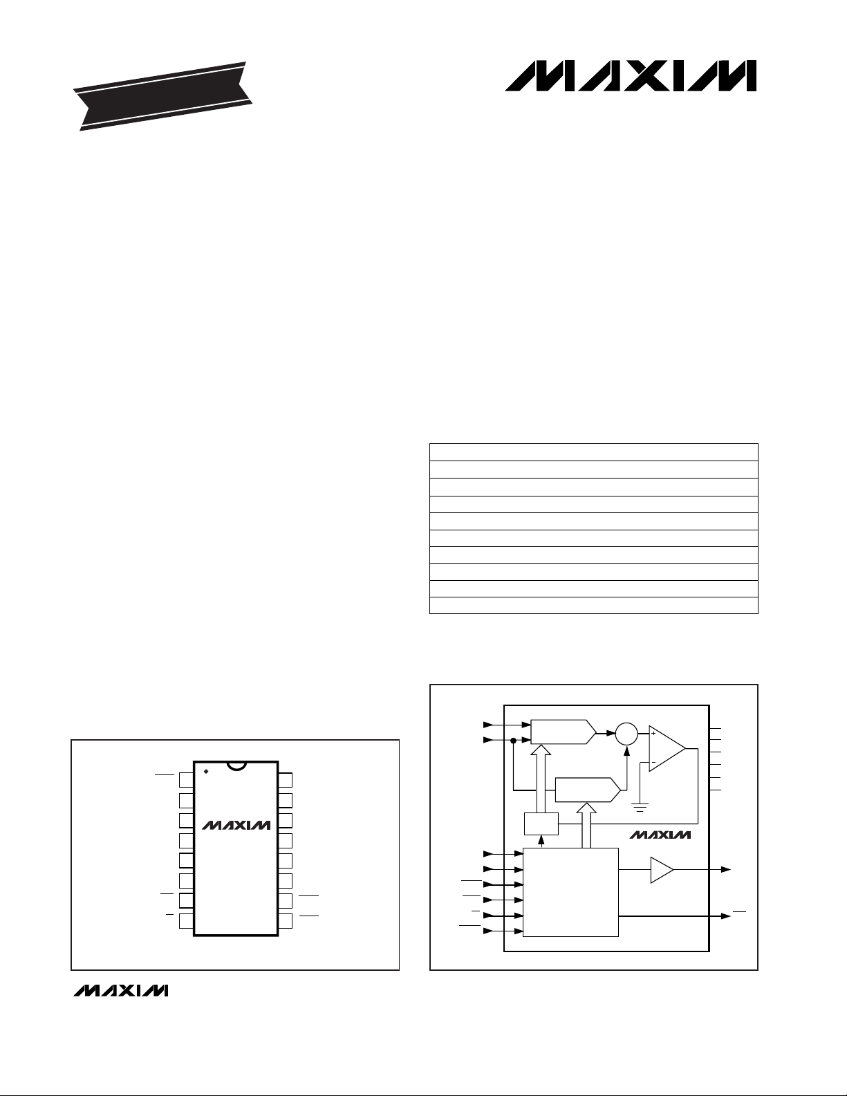
The MAX195 is available in 16-pin DIP, wide SO, and
ceramic sidebraze packages.
________________________Applications
Portable Instruments
Audio
Industrial Controls
Robotics
Multiple Transducer Measurements
Medical Signal Acquisition
Vibrations Analysis
Digital Signal Processing
____________________________Features
♦ 16 Bits, No Missing Codes
♦ 90dB SINAD
♦ 9.4µs Conversion Time
♦ 10µA (max) Shutdown Mode
♦ Built-In Track/Hold
♦ AC and DC Specified
♦ Unipolar (0V to V
REF
) and Bipolar (-V
REF
to V
REF
)
Input Range
♦ Three-State Serial-Data Output
♦ Small 16-Pin DIP, SO, and Ceramic SB Packages
______________Ordering Information
MAX195
16-Bit, 85ksps ADC with 10µA Shutdown
________________________________________________________________
Maxim Integrated Products
1
16
15
14
13
12
11
10
9
1
2
3
4
5
6
7
8
VDDA
VSSA
AGND
AIN
VDDD
SCLK
CLK
BP/UP/SHDN
TOP VIEW
MAX195
REF
VSSD
RESET
CONV
CS
EOC
DGND
DOUT
DIP/Wide SO/Ceramic SB
MAX195
AIN
REF
CONV
SCLK
CLK
BP/UP/SHDN
CS
RESET
VSSD
DGND
VDDD
VDDA
AGND
VSSA
DOUT
EOC
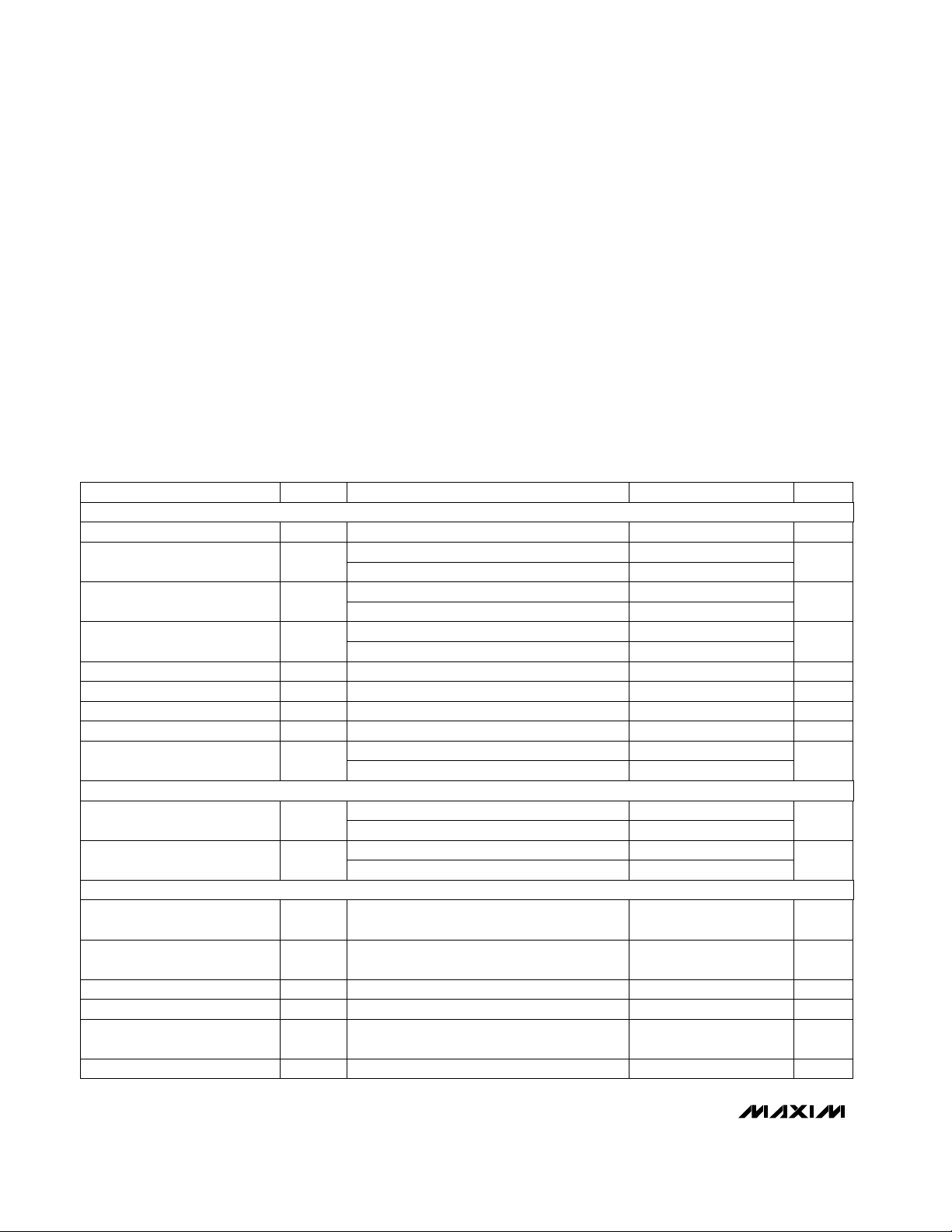
SAR
CONTROL LOGIC
COMPARATOR
CALIBRATION
DACs
THREE-STATE BUFFER
4
6
11
16
14
15
5
7
10
8
1
9
3
2
13
12
MAIN DAC
Σ
________________Functional Diagram
__________________Pin Configuration
19-0377; Rev 1; 12/97
PART
MAX195BCPE
MAX195BCWE
MAX195ACDE 0°C to +70°C
0°C to +70°C
0°C to +70°C
TEMP. RANGE PIN-PACKAGE
16 Plastic DIP
16 Wide SO
16 Ceramic SB
MAX195BC/D 0°C to +70°C Dice*
MAX195BEPE -40°C to +85°C 16 Plastic DIP
MAX195BEWE -40°C to +85°C 16 Wide SO
MAX195AEDE -40°C to +85°C 16 Ceramic SB
MAX195AMDE -55°C to +125°C 16 Ceramic SB**
MAX195BMDE -55°C to +125°C 16 Ceramic SB**
EVALUATION KIT
AVAILABLE
*
Dice are specified at TA= +25°C, DC parameters only.
**
Contact factory for availability and processing to MIL-STD-883.
For free samples & the latest literature: http://www.maxim-ic.com, or phone 1-800-998-8800.
For small orders, phone 408-737-7600 ext. 3468.
MAX195
16-Bit, 85ksps ADC with 10µA Shutdown
2 _______________________________________________________________________________________
ABSOLUTE MAXIMUM RATINGS
ELECTRICAL CHARACTERISTICS
(VDDD = VDDA = +5V, VSSD = VSSA = -5V, f
CLK
= 1.7MHz, V
REF
= +5V, TA= T
MIN
to T
MAX
, unless otherwise noted. Typical
values are at T
A
= +25°C.)
Stresses beyond those listed under “Absolute Maximum Ratings” may cause permanent damage to the device. These are stress ratings only, and functional
operation of the device at these or any other conditions beyond those indicated in the operational sections of the specifications is not implied. Exposure to
absolute maximum rating conditions for extended periods may affect device reliability.
VDDD to DGND .....................................................................+7V
VDDA to AGND......................................................................+7V
VSSD to DGND.........................................................+0.3V to -6V
VSSA to AGND.........................................................+0.3V to -6V
VDDD to VDDA, VSSD to VSSA..........................................±0.3V
AIN, REF ....................................(VSSA - 0.3V) to (VDDA + 0.3V)
AGND to DGND..................................................................±0.3V
Digital Inputs to DGND...............................-0.3V, (VDDA + 0.3V)
Digital Outputs to DGND............................-0.3V, (VDDA + 0.3V)
Continuous Power Dissipation (T
A
= +70°C)
Plastic DIP (derate 10.53mW/°C above +70°C) ............842mW
Wide SO (derate 9.52mW/°C above +70°C)..................762mW
Ceramic SB (derate 10.53mW/°C above +70°C)...........842mW
Operating Temperature Ranges
MAX195_C_E........................................................0°C to +70°C
MAX195_E_E .....................................................-40°C to +85°C
MAX195_MDE..................................................-55°C to +125°C
Storage Temperature Range.............................-65°C to +160°C
Lead Temperature (soldering, 10sec).............................+300°C
MAX195A
16 (t
CLK
)
TA= +25°C
TA= +25°C
Unipolar
V
REF
= 4.75V
MAX195A
MAX195B
MAX195A, V
REF
= 4.75V
VSSA = -5.25V to -4.75V, V
REF
= 4.75V
MAX195B, V
REF
= 4.75V
VDDA = 4.75V to 5.25V, V
REF
= 4.75V
CONDITIONS
MHz1.7f
CLK
Clock Frequency
(Notes 3, 4)
µs9.4t
CONV
Conversion Time
dB-90Peak Spurious Noise (Note 2)
dB-97 -90THD
Total Harmonic Distortion (up to
the 5th harmonic) (Note 2)
V
0 V
REF
Input Range
dB
65
Power-Supply Rejection
Ratio (VDDA and VSSA only)
65
±1
Bits16RESResolution
ppm/°C0.1Full-Scale Tempco
%FSRUnipolar Full-Scale Error ±0.0075
Unipolar/Bipolar Offset Tempco ppm/°C0.4
±0.003
%FSR
±0.004
INLIntegral Nonlinearity
±3
LSB
±4
Unipolar/Bipolar Offset Error
UNITSMIN TYP MAXSYMBOLPARAMETER
Unipolar
pF
250
Input Capacitance
TA= +25°C dB87 90SINAD
Signal-to-Noise plus Distortion
Ratio (Note 2)
MHz5f
SCLK
Serial Clock Frequency
Bipolar
Bipolar 125
-V
REF
V
REF
V
REF
= 4.75V %FSRBipolar Full-Scale Error ±0.018
MAX195B
LSB
±2
DNL
ACCURACY (Note 1)
ANALOG INPUT
DYNAMIC PERFORMANCE (fs= 85kHz, bipolar range AIN = -5V to +5V, 1kHz) (Note 1)
Differential Nonlinearity
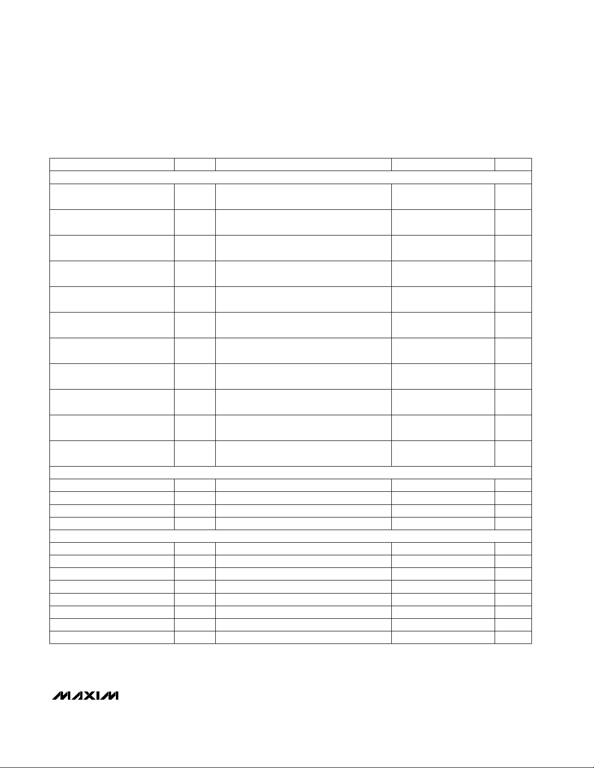
MAX195
16-Bit, 85ksps ADC with 10µA Shutdown
_______________________________________________________________________________________ 3
ELECTRICAL CHARACTERISTICS (continued)
(VDDD = VDDA = +5V, VSSD = VSSA = -5V, f
CLK
= 1.7MHz, V
REF
= +5V, TA= T
MIN
to T
MAX
, unless otherwise noted. Typical
values are at T
A
= +25°C.)
BP/UP/SHDN = open
VDDD = 5.25V
BP/UP/SHDN = open
BP/UP/SHDN = 0V
BP/UP/SHDN = VDDD
Digital inputs = 0 or 5V
VDDD = 4.75V
CONDITIONS
nA-100 +100
BP/UP/SHDN Max Allowed
Leakage, Mid Input
V2.75V
FLT
BP/UP/SHDN Voltage,
Floating
V1.5 VDDD - 1.5V
IM
BP/UP/SHDN
Mid Input Voltage
µA-4.0I
IL
BP/UP/SHDN
Input Current, Low
µA4.0I
IH
BP/UP/SHDN
Input Current, High
V0.5V
IL
BP/UP/SHDN
Input Low Voltage
V2.4V
IH
CLK, CS, CONV, RESET, SCLK
Input High Voltage
VVDDD - 0.5V
IH
BP/UP/SHDN
Input High Voltage
µA±10
CLK, CS, CONV, RESET, SCLK
Input Current
V0.8V
IL
CLK, CS, CONV, RESET, SCLK
Input Low Voltage
pF10
CLK, CS, CONV, RESET, SCLK
Input Capacitance (Note 3)
UNITSMIN TYP MAXSYMBOLPARAMETER
Output Low Voltage V
OL
VDDD = 4.75V, I
SINK
= 1.6mA 0.4 V
Output High Voltage V
OH
VDDD = 4.75V, I
SOURCE
= 1mA VDDD - 0.5 V
DOUT Leakage Current I
LKG
DOUT = 0 or 5V ±10 µA
Output Capacitance (Note 2) 10 pF
VDDD 4.75 5.25 V
VSSD -5.25 -4.75 V
VDDA By supply-rejection test 4.75 5.25 V
VSSA By supply-rejection test -5.25 -4.75 V
VDDD Supply Current I
DDD
VDDD = VDDA = 5.25V, VSSD = VSSA = -5.25V 2.5 4 mA
VSSD Supply Current I
SSD
VDDD = VDDA = 5.25V, VSSD = VSSA = -5.25V 0.9 2 mA
VDDA Supply Current I
DDA
VDDD = VDDA = 5.25V, VSSD = VSSA = -5.25V 3.8 5 mA
VSSA Supply Current I
SSA
VDDD = VDDA = 5.25V, VSSD = VSSA = -5.25V 3.8 5 mA
DIGITAL INPUTS (CLK, CS, CONV, RESET, SCLK, BP/UP/SHDN)
DIGITAL OUTPUTS (DOUT, EOC)
POWER REQUIREMENTS
MAX195
16-Bit, 85ksps ADC with 10µA Shutdown
4 _______________________________________________________________________________________
VDDD = VDDA = 5.25V, VSSD = VSSA = -5.25V
VDDD = VDDA = 5.25V, VSSD = VSSA = -5.25V,
BP/UP/SHDN = 0V
VDDD = VDDA = 5.25V, VSSD = VSSA = -5.25V,
BP/UP/SHDN = 0V
VDDD = VDDA = 5.25V, VSSD = VSSA = -5.25V,
BP/UP/SHDN = 0V
VDDD = VDDA = 5.25V, VSSD = VSSA = -5.25V,
BP/UP/SHDN = 0V
CONDITIONS
mW80Power Dissipation
µA0.1 5I
SSA
VSSA Shutdown Supply Current
µA0.1 5I
DDA
VDDA Shutdown Supply Current
µA1.6 5I
DDD
VDDD Shutdown Supply Current
(Note 5)
µA0.1 5I
SSD
VSSD Shutdown Supply Current
UNITSMIN TYP MAXSYMBOLPARAMETER
ELECTRICAL CHARACTERISTICS (continued)
(VDDD = VDDA = +5V, VSSD = VSSA = -5V, f
CLK
= 1.7MHz, V
REF
= +5V, TA= T
MIN
to T
MAX
, unless otherwise noted. Typical
values are at T
A
= +25°C.)
TIMING CHARACTERISTICS
(VDDD = VDDA = +5V, VSSD = VSSA = -5V, unless otherwise noted.)
Note 1: Accuracy and dynamic performance tests performed after calibration.
Note 2: Guaranteed by design, not tested.
Note 3: Tested with 50% duty cycle. Duty cycles from 25% to 75% at 1.7MHz are acceptable.
Note 4: See
External Clock
section.
Note 5: Measured in shutdown mode with CLK and SCLK low.
POWER REQUIREMENTS (cont.)
PARAMETER SYMBOL CONDITIONS
TA= +25°C
TYP
TA= 0°C to
+70°C
MIN MAX
TA= -40°C to
+85°C
MIN MAX
TA= -55°C to
+125°C
MIN MAX
UNITS
CONV Pulse Width
t
CW
20 30 35 ns
CONV to CLK Falling
Synchronization (Note 2)
t
CC1
10 10 10 ns
CONV to CLK Rising
Synchronization (Note 2)
t
CC2
40 40 ns
Data Access Time t
DV
CL= 50pF 80 80
40
ns
Bus Relinquish Time t
DH
CL= 10pF 40 40 40 ns
CLK to EOC High
t
CEH
CL= 50pF 300 300 350 ns
CLK to EOC Low
t
CEL
CL= 50pF 300 300 350 ns
CLK to DOUT Valid t
CD
CL= 50pF 100 350 100 375 100 400 ns
SCLK to DOUT Valid t
SD
CL= 50pF 20 140 20 160 20 160 ns
CS to SCLK Setup Time
t
CSS
75 75 75 ns
CS to SCLK Hold Time
t
CSH
-10 -10 -10 ns
Acquisition Time t
AQ
2.4 2.4 2.4 µs
Calibration Time t
CAL
14,000 x t
CLK
8.2 8.2 8.2 ms
RESET to CLK Setup Time
t
RCS
-40 -40 -40 ns
RESET to CLK Hold Time
t
RCH
120 120 120
Start-Up Time (Note 6) t
SU
Exiting
shutdown
50
ns
90
µs
Note 6: Settling time required after deasserting shutdown to achieve less than 0.1LSB additional error.
_______________Detailed Description
The MAX195 uses a successive-approximation register
(SAR) to convert an analog input to a 16-bit digital
code, which outputs as a serial data stream. The data
bits can be read either during the conversion, at the
CLK clock rate, or between conversions asynchronous
with CLK at the SCLK rate (up to 5Mbps).
The MAX195 includes a capacitive digital-to-analog
converter (DAC) that provides an inherent track/hold
input. The interface and control logic are designed for
easy connection to most microprocessors (µPs), limiting
the need for external components. In addition to the
SAR and DAC, the MAX195 includes a serial interface, a
sampling comparator used by the SAR, ten calibration
DACs, and control logic for calibration and conversion.
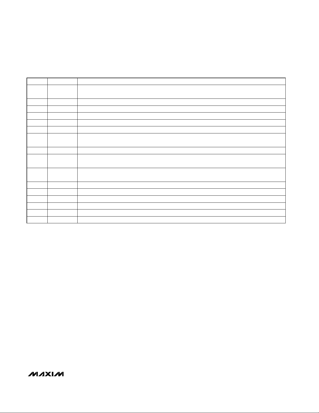
The DAC consists of an array of 16 capacitors with
binary weighted values plus one “dummy LSB” capacitor (Figure 1). During input acquisition in unipolar
mode, the array’s common terminal is connected to
AGND and all free terminals are connected to the input
signal (AIN). After acquisition, the common terminal is
disconnected from AGND and the free terminals are
disconnected from AIN, trapping a charge proportional
to the input voltage on the capacitor array.
The free terminal of the MSB (largest) capacitor is connected to the reference (REF), which pulls the common
terminal (connected to the comparator) positive.
Simultaneously, the free terminals of all other capacitors in the array are connected to AGND, which drives
the comparator input negative. If the analog input is
near V
REF
, connecting the MSB’s free terminal to REF
only pulls the comparator input slightly positive.
However, connecting the remaining capacitor’s free terminals to ground drives the comparator input well
below ground, so the comparator input is negative, the
comparator output is low, and the MSB is set high. If
the analog input is near ground, the comparator output
is high and the MSB is low.
Following this, the next largest capacitor is disconnected from AGND and connected to REF, and the comparator determines the next bit. This continues until all
bits have been determined. For a bipolar input range,
the MSB capacitor is connected to REF rather than AIN
during input acquisition, which results in an input range
of V
REF
to -V
REF
.
MAX195
16-Bit, 85ksps ADC with 10µA Shutdown
_______________________________________________________________________________________ 5
______________________________________________________________Pin Description
PIN NAME FUNCTION
1
BP/UP/SHDN
Bipolar/Unipolar/Shutdown Input. Three-state input selects bipolar or unipolar input range, or shutdown.
0V = shutdown, +5V = unipolar, floating = bipolar.
2 CLK Conversion Clock Input
3 SCLK Serial Clock Input is used to shift data out between conversions. May be asynchronous to CLK.
4 VDDD +5V Digital Power Supply
5 DOUT Serial Data Output, MSB first
6 DGND Digital Ground
7
EOC
End-of-Conversion/Calibration Output—normally low. Rises one clock cycle after the beginning of conversion
or calibration and falls one clock cycle after the end of either. May be used as an output framing signal.
8
CS
Chip-Select Input—active low. Enables the serial interface and the three-state data output (DOUT).
9
CONV
Convert-Start Input—active low. Conversion begins on the falling edge after CONV goes low if the input
signal has been acquired; otherwise, on the falling clock edge after acquisition.
10
RESET
Reset Input. Pulling RESET low places the ADC in an inactive state. Rising edge resets control logic and
begins calibration.
11 VSSD -5V Digital Power Supply
12 REF Reference Input, 0 to 5V
13 AIN Analog Input, 0 to V
REF
unipolar or ±V
REF
bipolar range
14 AGND Analog Ground
15 VSSA -5V Analog Power Supply
16 VDDA +5V Analog Power Supply
MAX195
Calibration
In an ideal DAC, each of the capacitors associated with
the data bits would be exactly twice the value of the
next smaller capacitor. In practice, this results in a
range of values too wide to be realized in an economically feasible size. The capacitor array actually consists
of two arrays, which are capacitively coupled to reduce
the LSB array’s effective value. The capacitors in the
MSB array are production trimmed to reduce errors.
Small variations in the LSB capacitors contribute
insignificant errors to the 16-bit result.
Unfortunately, trimming alone does not yield 16-bit performance or compensate for changes in performance
due to changes in temperature, supply voltage, and
other parameters. For this reason, the MAX195 includes
a calibration DAC for each capacitor in the MSB array.
These DACs are capacitively coupled to the main DAC
output and offset the main DAC’s output according to
the value on their digital inputs. During calibration, the
correct digital code to compensate for the error in each
MSB capacitor is determined and stored. Thereafter,
the stored code is input to the appropriate calibration
DAC whenever the corresponding bit in the main DAC
is high, compensating for errors in the associated
capacitor.
The MAX195 calibrates automatically on power-up. To
reduce the effects of noise, each calibration experiment
is performed many times and the results are averaged.
Calibration requires about 14,000 clock cycles, or
8.2ms at the highest clock (CLK) speed (1.7MHz). In
addition to the power-up calibration, bringing RESET
low halts MAX195 operation, and bringing it high again
initiates a calibration (Figure 2).
16-Bit, 85ksps ADC with 10µA Shutdown
6 _______________________________________________________________________________________
MSB
AIN
REF
AGND
DUMMYLSB
32,768C
16,384C 4C 2C C C
EOC
CLK
RESET
CALIBRATION
BEGINS
CALIBRATION
ENDS
MAX195
OPERATION HALTS
t
CAL
t
RCS
t
RCH
Figure 1. Capacitor DAC Functional Diagram
Figure 2. Initiating Calibration
If the power supplies do not settle within the MAX195’s
power-on delay (500ns minimum), power-up calibration
may begin with supply voltages that differ from the final
values and the converter may not be properly calibrated. If so, recalibrate the converter (pulse RESET low)
before use. For best DC accuracy, calibrate the
MAX195 any time there is a significant change in supply voltages, temperature, reference voltage, or clock
characteristics (see
External Clock
section) because
these parameters affect the DC offset. If linearity is the
only concern, much larger changes in these parameters can be tolerated.
Because the calibration data is stored digitally, there is
no need either to perform frequent conversions to maintain accuracy or to recalibrate if the MAX195 has been
held in shutdown for long periods. However, recalibration is recommended if it is likely that ambient temperature or supply voltages have significantly changed
since the previous calibration.
Digital Interface
The digital interface pins consist of BP/UP/SHDN, CLK,
SCLK, EOC, CS, CONV, and RESET.
BP/UP/SHDN is a three-level input. Leave it floating to
configure the MAX195’s analog input in bipolar mode
(AIN = -V
REF
to V
REF
) or connect it high for a unipolar
input (AIN = 0V to V
REF
). Bringing BP/UP/SHDN low
places the MAX195 in its 10µA shutdown mode.
A logic low on RESET halts MAX195 operation. The ris-
ing edge of RESET initiates calibration as described in
the
Calibration
section above.
Begin a conversion by bringing CONV low. After conversion begins, additional convert start pulses are
ignored. The convert signal must be synchronized with
CLK. The falling edge of CONV must occur during the
period shown in Figures 3 and 4. When CLK is not
directly controlled by your processor, two methods of
ensuring synchronization are to drive CONV from EOC
(continuous conversions) or to gate the conversion-start
signal with the conversion clock so that CONV can go
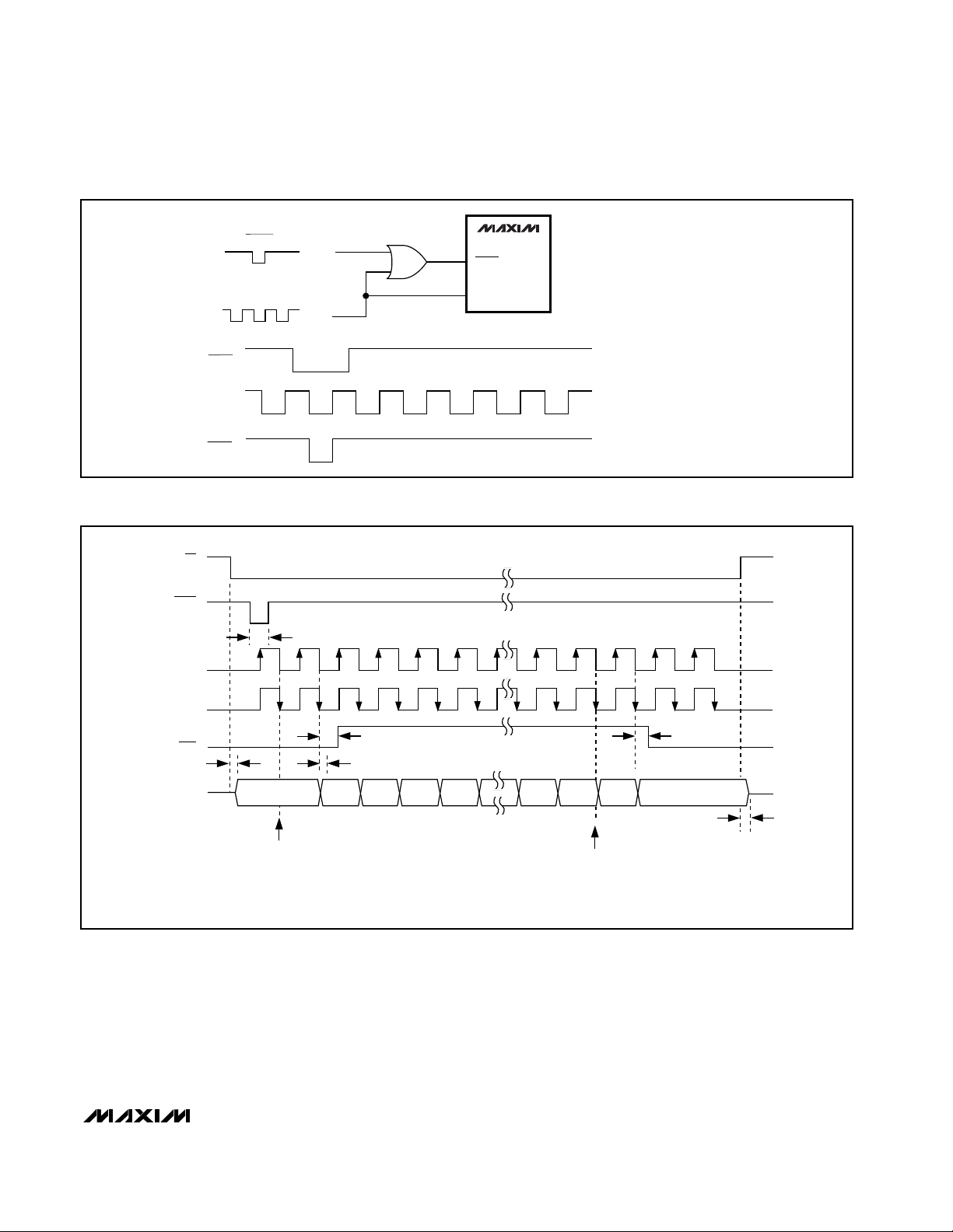
low only while CLK is low (Figure 5). Ensure that the
maximum propagation delay through the gate is less
than 40ns.
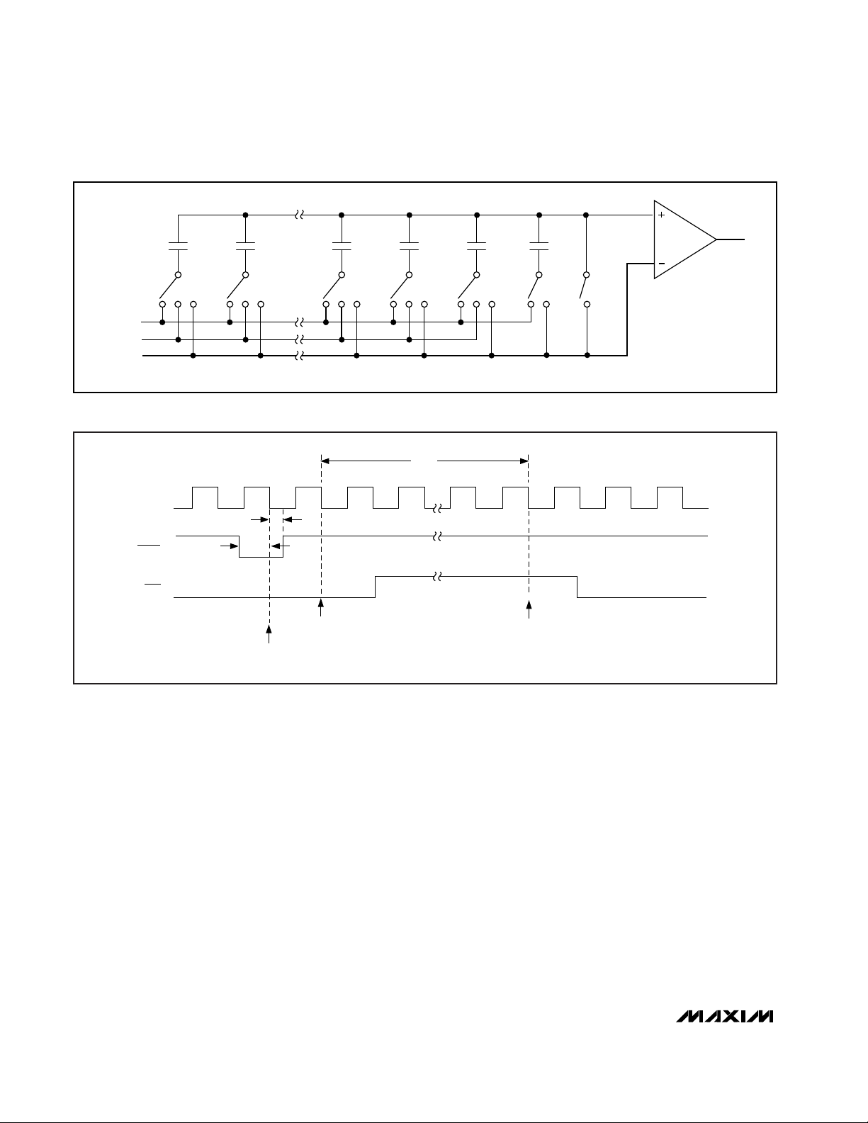
The MAX195 automatically ensures four CLK periods
for track/hold acquisition. If, when CONV is asserted, at
least three clock (CLK) cycles have passed since the
end of the previous conversion, a conversion will begin
on CLK’s next falling edge and EOC will go high on the
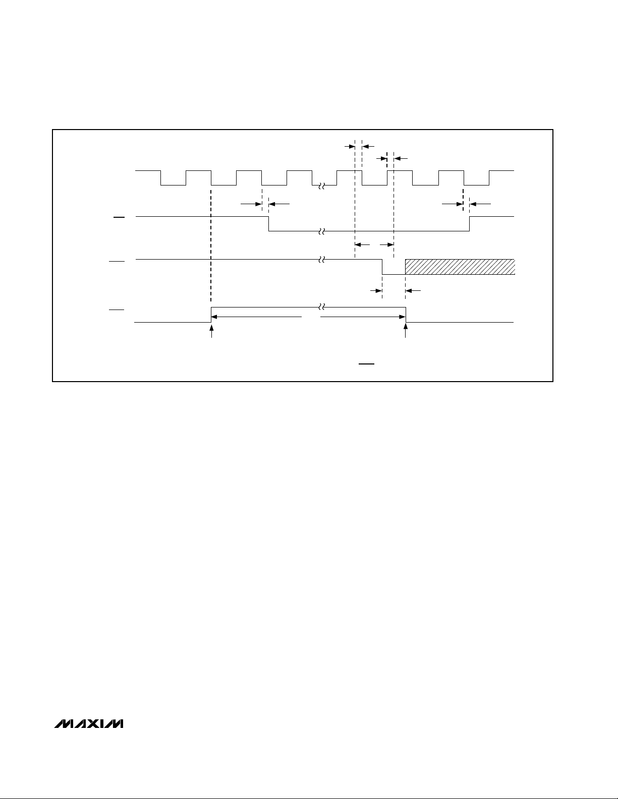
following falling CLK edge (Figure 3). If, when convert
is asserted, less than three clock cycles have passed,
a conversion will begin on the fourth falling clock edge
MAX195
16-Bit, 85ksps ADC with 10µA Shutdown
_______________________________________________________________________________________ 7
TRACK/HOLD
CLK
CONVERSION
BEGINS
CONVERSION
ENDS
t
AQ
*
*
THE FALLING EDGE OF CONV MUST OCCUR IN THIS REGION
t
CEL
t
CW
t
CEH
t
CC2
t
CC1
EOC
CONV
Figure 3. Initiating Conversions—At least 3 CLK cycles since end of previous conversion.
MAX195
after the end of the previous conversion and EOC will
go high on the following CLK falling edge (Figure 4).
External Clock
The conversion clock (CLK) should have a duty cycle
between 25% and 75% at 1.7MHz (the maximum clock
frequency). For lower frequency clocks, ensure the minimum high and low times exceed 150ns. The minimum
clock rate for accurate conversion is 125Hz for temperatures up to +70°C or 1kHz at +125°C due to leakage
of the sampling capacitor array. In addition, CLK
should not remain high longer than 50ms at temperatures up to +70°C or 500µs at +125°C. If CLK is held
high longer than this, RESET must be pulsed low to initiate a recalibration because it is possible that state
information stored in internal dynamic memory may be
lost. The MAX195’s clock can be stopped indefinitely if
it is held low.
If the frequency, duty cycle, or other aspects of the
clock signal’s shape change, the offset created by coupling between CLK and the analog inputs (AIN and
REF) changes. Recalibration corrects for this offset and
restores DC accuracy.
Output Data
The conversion result, clocked out MSB first, is available on DOUT only when CS is held low. Otherwise,
DOUT is in a high-impedance state. There are two ways
to read the data on DOUT. To read the data bits as they
are determined (at the CLK clock rate), hold CS low
during the conversion. To read results between conversions, hold CS low and clock SCLK at up to 5MHz.
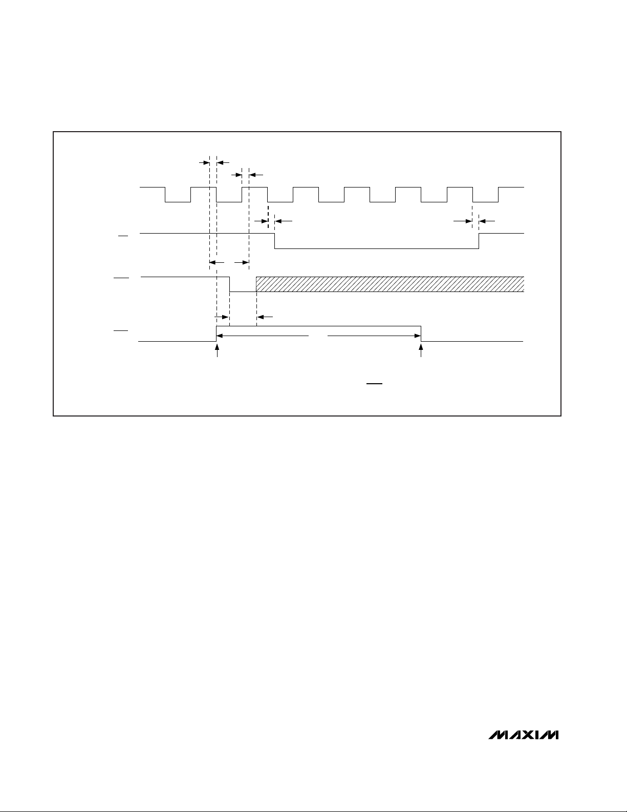
If you read the serial data bits as they are determined,
EOC frames the data bits (Figure 6). Conversion begins
with the first falling CLK edge, after CONV goes low
and the input signal has been acquired. Data bits are
shifted out of DOUT on subsequent falling CLK edges.
Clock data in on CLK’s rising edge or, if the clock
speed is greater than 1MHz, on the following falling
edge of CLK to meet the maximum CLK-to-DOUT timing specification. See the
Operating Modes and
SPI™/QSPI™ Interfaces
section for additional information. Reading the serial data during the conversion
results in the maximum conversion throughput,
because a new conversion can begin immediately after
the input acquisition period following the previous conversion.
16-Bit, 85ksps ADC with 10µA Shutdown
8 _______________________________________________________________________________________
TRACK/HOLD
CLK
CONVERSION
BEGINS
CONVERSION
ENDS
t
AQ
*
*
THE FALLING EDGE OF CONV MUST OCCUR IN THIS REGION
t
CEL
t
CW
t
CEH
t
CC2
t
CC1
EOC
CONV
Figure 4. Initiating Conversions—Less than 3 CLK cycles since end of previous conversion.
SPI/QSPI are trademarks of Motorola Corp.
If you read the data bits between conversions, you can:
1) count CLK cycles until the end of the conversion, or
2) poll EOC to determine when the conversion is
finished, or
3) generate an interrupt on EOC’s falling edge.
Note that the MSB conversion result appears at DOUT
after CS goes low, but before the first SCLK pulse.
Each subsequent SCLK pulse shifts out the next conversion bit. The 15th SCLK pulse shifts out the LSB.
Additional clock pulses shift out zeros.
MAX195
16-Bit, 85ksps ADC with 10µA Shutdown
_______________________________________________________________________________________ 9
CLK
START
CONV
MAX195
CONV
START
CLK
SEE
DIGITAL INTERFACE
SECTION
Figure 5. Gating CONV to Synchronize with CLK
Figure 6. Output Data Format, Reading Data During Conversion (Mode 1)
CS
CONV
t
CW
CLK
(CASE 1)
CLK
(CASE 2)
EOC
DOUT
CASE 1: CLK IDLES LOW, DATA LATCHED ON RISING EDGE (CPOL = 0, CPHA = 0)
CASE 2: CLK IDLES LOW, DATA LATCHED ON FALLING EDGE (CPOL = 0, CPHA = 1)
NOTE: ARROWS ON CLK TRANSITIONS INDICATE LATCHING EDGE
t
DV
B15 FROM PREVIOUS
CONVERSION
CONVERSION
BEGINS
t
CEH
t
CD
B15
B14 B13 B12 B2 B1 B0 B15
MSB
LSB
CONVERSION
ENDS
t
CEL
t
DH

MAX195
Data is clocked out on SCLK’s falling edge. Clock
data in on SCLK’s rising edge or, for clock speeds
above 2.5MHz, on the following falling edge to meet
the maximum SCLK-to-DOUT timing specification
(Figure 7). The maximum SCLK speed is 5MHz. See
the
Operating Modes and SPI/QSPI Interfaces
section
for additional information. When the conversion clock
is near its maximum (1.7MHz), reading the data after
each conversion (during the acquisition time) results
in lower throughput (about 70ksps max) than reading
the data during conversions, because it takes longer
than the minimum input acquisition time (four cycles
at 1.7MHz) to clock 16 data bits at 5Mbps. After the
data has been clocked in, leave some time (about
1µs) for any coupled noise on AIN to settle before
beginning the next conversion.
Whichever method is chosen for reading the data, conversions can be individually initiated by bringing CONV
low, or they can occur continuously by connecting EOC
to CONV. Figure 8 shows the MAX195 in its simplest
operational configuration.
16-Bit, 85ksps ADC with 10µA Shutdown
10 ______________________________________________________________________________________
EOC
CS
SCLK
(CASE 1)
SCLK
(CASE 2)
CASE 1: SCLK IDLES LOW, DATA LATCHED ON RISING EDGE (CPOL = 0, CPHA = 0)
CASE 2: SCLK IDLES LOW, DATA LATCHED ON FALLING EDGE (CPOL = 0, CPHA = 1)
CASE 3: SCLK IDLES HIGH, DATA LATCHED ON FALLING EDGE (CPOL = 1, CPHA = 0)
NOTE: ARROWS ON SCLK TRANSITIONS INDICATE LATCHING EDGE
DOUT
SCLK
(CASE 3)
t
CONV
t
DH
t
SD
t
DV
MSB LSB
B15
B14 B13 B12 B3 B2 B1
B0
B11
t
CSS
t
CSH
Figure 7. Output Data Format, Reading Data Between Conversions (Mode 2)
Figure 8. MAX195 in the Simplest Operating Configuration
+5V
1
2
3
4
5
6
7
8
0.1µF
BP/UP/
SHDN
CLK
SCLK
VDDD
DOUT
DGND
EOC
CS
MAX195
VDDA
VSSA
AGND
AIN
REF
VSSD
RESET
CONV
0.1µF
16
15
14
13
12
11
10
9
ANALOG
INPUT
REFERENCE
(0V TO VDDA)
10µF
CONVERSION
CLOCK
10µF
-5V

MAX195
16-Bit, 85ksps ADC with 10µA Shutdown
______________________________________________________________________________________ 11
BRIDGE
INSTRUMENTATION
AMPLIFIER
+5V
AIN
MAX195
VDDA
AGND
47µF
LOW ESR
0.1µF
CERAMIC
REF
COMPANY CAPACITOR FACTORY FAX [COUNTRY CODE] USA TELEPHONE
Sprague
595D series,
592D series
1-603-224-1430 603-224-1961
AVX TPS series 1-207-283-1941 800-282-4975
Sanyo
OS-CON series,
MVGX series
81-7-2070-1174 619-661-6835
Nichicon PL series 1-708-843-2798 708-843-7500
Figure 9. Ratiometric Measurement Without an Accurate Reference
Table 1. Low-ESR Capacitor Suppliers
__________Applications Information
Reference
The MAX195 reference voltage range is 0V to VDDA.
When choosing the reference voltage, the MAX195’s
equivalent input noise (40µV
RMS
in unipolar mode,
80µV
RMS
in bipolar mode) should be considered. Also, if
V
REF
exceeds VDDA, errors will occur due to the internal
protection diodes that will begin to conduct, so use caution when using a reference near VDDA (unless V
REF
and VDDA are virtually identical). V
REF
must never
exceed its absolute maximum rating (VDDA + 0.3V).
The MAX195 needs a good reference to achieve its
rated performance. The most important requirement is
that the reference must present a low impedance to the
REF input. This is often achieved by buffering the reference through an op amp and bypassing the REF input
with a large (1µF to 47µF), low-ESR capacitor in parallel
with a 0.1µF ceramic capacitor. Low-ESR capacitors
are available from the manufacturers listed in Table 1.
The reference must drive the main conversion DAC
capacitors as well as the capacitors in the calibration
DACs, all of which may be switching between GND and
REF at the conversion clock frequency. The total
capacitive load presented can exceed 1000pF and,
unlike the analog input (AIN), REF is sampled continuously throughout the conversion.
The first step in choosing a reference circuit is to
decide what kind of performance is required. This often
suggests compromises made in the interests of cost
and size. It is possible that a system may not require an
accurate reference at all. If a system makes a ratiometric measurement such as Figure 9’s bridge circuit, any
relatively noise-free voltage that presents a low impedance at the REF input will serve as a reference. The
+5V analog supply suffices if you use a large, lowimpedance bypass capacitor to keep REF stable during switching of the capacitor arrays. Do not place a
resistance between the +5V supply and the bypass
capacitor, because it will cause linearity errors due to
the dynamic REF input current, which typically ranges
from 300µA to 400µA.
Figure 10 shows a more typical scheme that provides
good AC accuracy. The MAX874’s initial accuracy can

MAX195
be improved by trimming, but the drift is too great to
provide good stability over temperature. The MAX427
buffer provides the necessary drive current to stabilize
the REF input quickly after capacitance changes.
The reference inaccuracies contribute additional fullscale error. A reference with less than 1⁄
2
16
total error
(15 parts per million) over the operating temperature
range is required to limit the additional error to less
than 1LSB. The MAX6241 achieves a drift specification
of 1ppm/°C (typ). This allows reasonable temperature
changes with less than 1LSB error. While the
MAX6241’s initial-accuracy specification (0.02%)
results in an offset error of about ±14LSB, the reference
voltage can be trimmed or the offset can be corrected
in software if absolute DC accuracy is essential. Figure
11’s circuit provides outstanding temperature stability
and also provides excellent DC accuracy if the initial
error is corrected.
16-Bit, 85ksps ADC with 10µA Shutdown
12 ______________________________________________________________________________________
14
16
15
12
MAX195
MAX427
AGNDVSSA
VDDA
4
4
7
6
8
6
2
2
3
MAX874
GND
V
IN
COMP
V
OUT
4.096V
+15V
-15V
47µF
LOW ESR
0.1µF
0.1µF
0.1µF
0.1µF
1000pF
0.1µF
0.1µF
1k
10Ω
2k
REF
1N914
1N914
10Ω
-5V
+5V
Figure 10. Typical Reference Circuit for AC Accuracy
Figure 11. High-Accuracy Reference
≥ 8V
V
IN
2
IN
2.2µF
1µF
MAX6241
3
NR
GND
4 14
OUT
TRIM
6
5
10k
2.2µF
0.1µF
12
REF
MAX195
AGND

MAX195
16-Bit, 85ksps ADC with 10µA Shutdown
______________________________________________________________________________________ 13
INPUT
SIGNAL
1N914
DIODE
CLAMPS
+5V
AIN
MAX195
-5V
VSSA
VDDA
+15V
-15V
10Ω
Figure 12. Analog Input Protection for Overvoltage or Improper Supply Sequence
REF and AIN Input Protection
The REF and AIN signals should not exceed the
MAX195 supply rails. If this can occur, diode clamp the
signal to the supply rails. Use silicon diodes and a 10Ω
current-limiting resistor (Figures 10 and 12) or Schottky
diodes without the resistor.
When using the current-limiting resistor, place the resistor between the appropriate input (AIN or REF) and any
bypass capacitor. While this results in AC transients at
the input due to dynamic input currents, the transients
settle quickly and do not affect conversion results.
Improperly placing the bypass capacitor directly at the
input forms an RC lowpass filter with the current-limiting
resistor, which averages the dynamic input current and
causes linearity errors.
Analog Input
The MAX195 uses a capacitive DAC that provides an
inherent track/hold function. The input impedance is
typically 30Ω in series with 250pF in unipolar mode and
50Ω in series with 125pF in bipolar mode.
Input Range
The analog input range can be either unipolar (0V to
V
REF
) or bipolar (-V
REF
to V
REF
), depending on the
state of the BP/UP/SHDN pin (see
Digital Interface
section). The reference range is 0V to VDDA. When choosing the reference voltage, the equivalent MAX195 input
noise (40µV
RMS
in unipolar mode, 80µV
RMS
in bipolar
mode) should be considered.
Input Acquisition and Settling
Four conversion-clock periods are allocated for acquiring the input signal. At the highest conversion rate, four
clock periods is 2.4µs. If more than three clock cycles
have occurred since the end of the previous conversion, conversion begins on the next falling clock edge
after CONV goes low. Otherwise, bringing CONV low
begins a conversion on the fourth falling clock edge
after the previous conversion. This scheme ensures the
minimum input acquisition time is four clock periods.
Most applications require an input buffer amplifier. If
the input signal is multiplexed, the input channel should
be switched near the beginning of a conversion, rather
than near the end of or after a conversion (Figure 13).
This allows time for the input buffer amplifier to respond
to a large step change in input signal. The input amplifier must have a high enough slew rate to complete the
required output voltage change
before
the beginning of
the acquisition time.
At the beginning of acquisition, the capacitive DAC is
connected to the amplifier output, causing some output
disturbance. Ensure that the sampled voltage has settled to within the required limits before the end of the
acquisition time. If the frequency of interest is low, AIN
can be bypassed with a large enough capacitor to
charge the capacitive DAC with very little change in
voltage (Figure 14). However, for AC use, AIN must be
driven by a wideband buffer (at least 10MHz), which
must be stable with the DAC’s capacitive load (in parallel with any AIN bypass capacitor used) and also must
settle quickly (Figure 15 or 16).

MAX195
16-Bit, 85ksps ADC with 10µA Shutdown
14 ______________________________________________________________________________________
MAX400
4
7
6
2
3
IN
+15V
-15V
1.0µF
0.1µF
0.1µF
1000pF
1k
100Ω
AIN
1N914
1N914
+5V
-5V
10Ω
Figure 14. MAX400 Drives AIN for Low-Frequency Use
EOC
A0
A1
CLK
CHANGE MUX INPUT HERE
CONVERSION
IN1
A0 A1
IN2
IN3
IN4
OUT
ACQUISITION
MAX195
4-TO-1
MUX
EOC
AIN
Figure 13. Change multiplexer input near beginning of conversion to allow time for slewing and settling.

Digital Noise
Digital noise can easily be coupled to AIN and REF. The
conversion clock (CLK) and other digital signals that are
active during input acquisition contribute noise to the conversion result. If the noise signal is synchronous to the
sampling interval, an effective input offset is produced.
Asynchronous signals produce random noise on the input,
whose high-frequency components may be aliased into
the frequency band of interest. Minimize noise by presenting a low impedance (at the frequencies contained in the
noise signal) at the inputs. This requires bypassing AIN to
AGND, or buffering the input with an amplifier that has a
small-signal bandwidth of several megahertz, or preferably both. AIN has a bandwidth of about 16MHz.
Offsets resulting from synchronous noise (such as the
conversion clock) are canceled by the MAX195’s calibration scheme. However, because the magnitude of
the offset produced by a synchronous signal depends
on the signal’s shape, recalibration may be appropriate
if the shape or relative timing of the clock or other digital signals change, as might occur if more than one
clock signal or frequency is used.
Distortion
Avoid degrading dynamic performance by choosing an
amplifier with distortion much less than the MAX195’s
THD (-97dB, or 0.0014%) at frequencies of interest. If
the chosen amplifier has insufficient common-mode
rejection, which results in degraded THD performance,
use the inverting configuration (positive input grounded) to eliminate errors from this source. Low temperature-coefficient, gain-setting resistors reduce linearity
errors caused by resistance changes due to self-heat-
ing. Also, to reduce linearity errors due to finite amplifier
gain, use an amplifier circuit with sufficient loop gain at
the frequencies of interest (Figures 14, 15, 16).
DC Accuracy
If DC accuracy is important, choose a buffer with an
offset much less than the MAX195’s maximum offset
(±3LSB = ±366µV for a ±4V input range), or whose
offset can be trimmed while maintaining good stability
over the required temperature range.
Recommended Circuits
Figure 14 shows a good circuit for DC and low-frequency use. The MAX400 has very low offset (10µV) and
drift (0.2µV/°C), and low voltage noise (10nV/√Hz) as
well. However, its gain-bandwidth product (GBW) is
much too low to drive AIN directly, so the analog input
is bypassed to present a low impedance at high frequencies. The large bypass capacitor is isolated from
the amplifier output by a 100Ω resistor, which provides
additional noise filtering. Since the ±15V supplies
exceed the AIN range, add protection diodes at AIN
(see
REF and AIN Input Protection
section).
Figure 15 shows a wide-bandwidth amplifier (MAX427)
driving a wideband video buffer, which is capable of
driving AIN and a small bypass capacitor (for noise
reduction) directly. The video buffer is inside the
MAX427’s feedback loop, providing good DC accuracy, while the buffer’s low output impedance and highcurrent capability provide good AC performance. AIN is
diode-clamped to the ±5V rails to prevent overvoltage.
The MAX427’s 15µV maximum offset voltage, 0.8µV/°C
maximum drift, and less than 5nV/√Hz noise specifications make this an excellent choice for AC/DC use.
MAX195
16-Bit, 85ksps ADC with 10µA Shutdown
______________________________________________________________________________________ 15
MAX427
4
7
6
2
2
3
IN
+15V
-15V
0.0033µF
0.1µF
0.1µF
ELANTEC
EL2003
4
1
7
+15V
-15V
0.1µF
0.1µF
100pF
1k
1k
1N914
1N914
+5V
-5V
AIN
10Ω
Figure 15. AIN Buffer for AC/DC Use

MAX195
If ±15V supplies are unavailable, Figure 16’s circuit
works very well with the ±5V analog supplies used by
the MAX195. The MAX410 has a minimum ±3.5V common-mode input range, with a similar output voltage
swing, which allows use of a reference voltage up to
3.5V. The offset voltage (250µV) is about 2LSB. The
drift (1µV/°C), unity-gain bandwidth (28MHz), and low
voltage noise (2.4nV/√Hz) are appropriate for 16-bit
performance.
Operating Modes and SPI/QSPI Interfaces
The two basic interface modes are defined according
to whether serial data is received during the conversion
(clocked with CLK, SCLK unused) or in bursts between
conversions (clocked with SCLK). Each mode is presented interfaced to a QSPI processor, but is also compatible with SPI.
Mode 1 (Simultaneous
Conversion and Data Transfer)
In this mode, each data bit is read from the MAX195
during the conversion as it is determined. SCLK is
grounded and CLK is used as both the conversion
clock and the serial data clock. Figure 17 shows a
QSPI processor connected to the MAX195 for use in
this mode and Figure 18 is the associated timing diagram.
In addition to the standard QSPI interface signals, general I/O lines are used to monitor EOC and to drive
BP/UP/SHDN and RESET. The two general output pins
may not be necessary for a given application and, if I/O
lines are unavailable, the EOC connection can be omitted as well.
The EOC signal is monitored during calibration to
determine when calibration is finished and before
beginning a conversion to ensure the MAX195 is not in
mid-conversion, but it is possible for a system to ignore
EOC completely. On power-up or after pulsing RESET
low, the µP must provide 14,000 CLK cycles to complete the calibration sequence (Figure 2). One way to
do this is to toggle CLK and monitor EOC until it goes
low, but it is possible to simply count 14,000 CLK
cycles to complete the calibration. Similarly, it is
unnecessary to check the status of EOC before beginning a conversion if you are sure the last conversion is
complete. This can be done by ensuring that every
conversion consists of at least 20 CLK cycles.
Data is clocked out of the MAX195 on CLK’s falling
edge and can be clocked into the µP on the rising
edge or the following falling edge. If you clock data in
on the rising edge (SPI/QSPI with CPOL = 0 and CPHA
= 0; standard MicroWire™: Hitachi H8), the maximum
CLK rate is given by:
where tCDis the MAX195’s CLK-to-DOUT valid delay
and tSDis the data setup time for your µP.
f = /
1
t + t
CLK(max)
1
2
CD SD
16-Bit, 85ksps ADC with 10µA Shutdown
16 ______________________________________________________________________________________
MAX195
QSPI
GPT
BP/UP/SHDN
CLK
SCLK
EOC
DOUT
RESET
CONV
CS
*OC3
SCK
*IC1
MISO
*OC2
* THE USE OF THESE SIGNALS ADDS FLEXIBILITY AND FUNCTIONALITY
BUT IS NOT REQUIRED TO IMPLEMENT THE INTERFACE.
PCS0
Figure 17. MAX195 Connection to QSPI Processor Clocking
Data Out During Conversions
MAX410
4
7
6
2
3
IN
+5V
-5V
0.1µF
0.01µF
22Ω
510Ω
0.1µF
AIN
Figure 16. ±5V Buffer for AC/DC Use Has ±3.5V Swing
MicroWire is a trademark of National Semiconductor Corp.

If clocking data in on the falling edge (CPOL = 0,
CPHA = 1), the maximum CLK rate is given by:
Do not exceed the maximum CLK frequency given in
the
Electrical Characteristics
table. To clock data in on
the falling edge, your processor hold time must not
exceed tCDminimum (100ns).
While QSPI can provide the required 20 CLK cycles as
two continuous 10-bit transfers, SPI is limited to 8-bit
transfers. This means that with SPI, a conversion must
consist of three 8-bit transfers. Ensure that the pauses
between 8-bit operations at your selected clock rate
are short enough to maintain a 20ms or shorter conversion time, or the leakage of the capacitive DAC may
cause errors.
Complete source code for the Motorola 68HC16 and
the MAX195 evaluation kit (EV kit) using this mode is
available with the MAX195 EV kit.
Mode 2 (Asynchronous Data Transfer)
This mode uses a conversion clock (CLK) and a serial
clock (SCLK). The serial data is clocked out between
conversions, which reduces the maximum throughput
for high CLK rates, but may be more convenient for
some applications. Figure 19 is a block diagram with a
QSPI processor (Motorola 68HC16) connected to the
MAX195. Figure 20 shows the associated timing diagram. Figure 21 gives an assembly language listing for
this arrangement.
f =
1
t + t
CLK(max)
CD SD
MAX195
16-Bit, 85ksps ADC with 10µA Shutdown
______________________________________________________________________________________ 17
EOC
CLK
t
CD
t
DV
DATA LATCHED:
t
DH
CS, CONV
DOUT
B15 FROM PREVIOUS
CONVERSION
B15 B15B2B14 B1 B0
Figure 19. MAX195 Connection to QSPI Processor Clocking
Data Out with SCLK Between Conversions
Figure 18. Timing Diagram for Circuit of Figure 17 (Mode 1)
QSPI
PCS0
SCK
MISO
OC3
GPT
IC1
OC2
START
1.3µs
74HC32
CS
MAX195
SCLK
DOUT
BP/UP/SHDN
EOC
RESET
CONV
CLKIC3
1.7MHz

MAX195
An OR gate is used to synchronize the “start” signal to
the asynchronous CLK, as described in the
External
Clock
section. As with Mode 1, the QSPI processor must
run CLK during calibration and either count CLK cycles
or, as is done here, monitor EOC to determine when calibration is complete. Also, EOC is polled by the µP to
determine when a conversion result is available. When
EOC goes low, data is clocked out at the highest QSPI
data rate (4.19Mbps). After the data is transferred, a
new conversion can be initiated whenever desired.
The timing specification for SCLK-to-DOUT valid (tSD)
imposes some constraints on the serial interface. At
SCLK rates up to 2.5Mbps, data is clocked out of the
MAX195 by a falling edge of SCLK and may be
clocked into the µP by the next rising edge (CPOL = 0,
CPHA = 0). For data rates greater than 2.5Mbps (or for
lower rates, if desired) it is necessary to clock data out
of the MAX195 on SCLK’s falling edge and to clock it
into the µP on SCLK’s next falling edge (CPOL = 0,
CPHA = 1). Also, your processor hold time must not
exceed tSDminimum (20ns). As with CLK in mode 1,
maximum SCLK rates may not be possible with some
interface specifications that are subsets of SPI.
Supplies, Layout, Grounding
and Bypassing
For best system performance, use printed circuit
boards with separate analog and digital ground planes.
Wire-wrap boards are not recommended. The two
ground planes should be tied together at the lowimpedance power-supply source and at the MAX195
(Figure 22.) If the analog and digital supplies come
from the same source, isolate the digital supply from
the analog supply with a low-value resistor (10Ω).
Constraints on sequencing the four power supplies are
as follows.
• Apply VDDA before VDDD.
• Apply VSSA before VSSD.
• Apply AIN and REF after VDDA and VSSA are present.
• The power supplies should settle within the
MAX195’s power-on delay (minimum 500ns) or you
should recalibrate the converter (pulse RESET low)
before use.
16-Bit, 85ksps ADC with 10µA Shutdown
18 ______________________________________________________________________________________
CS
CLK
START
588ns
239ns
CONVERSION TIME
4.19MHz
1.3µs 9.4µs 17µs* 5.1µs
4µs
EOC
SCLK
DOUT
B15 B3 B2B13B14 B1 B0
* INTERRUPT LATENCY OF THE PROCESSOR
Figure 20. Timing Diagram for Circuit of Figure 19 (Mode 2)

MAX195
16-Bit, 85ksps ADC with 10µA Shutdown
______________________________________________________________________________________ 19
Figure 21. MAX195 Code Listing for 68HC16 Module and Circuit of Figure 19

MAX195
16-Bit, 85ksps ADC with 10µA Shutdown
20 ______________________________________________________________________________________
Figure 21. MAX195 Code Listing for 68HC16 Module and Circuit of Figure 19 (continued)

MAX195
16-Bit, 85ksps ADC with 10µA Shutdown
______________________________________________________________________________________ 21
Be sure that digital return currents do not pass through
the analog ground and that return-current paths are low
impedance. A 5mA current flowing through a PC board
ground trace impedance of only 0.05Ω creates an error
voltage of about 250µV, or about 2LSBs error with a
±4V full-scale system.
The board layout should ensure as much as possible
that digital and analog signal lines are kept separate.
Do not run analog and digital (especially clock) lines
parallel to one another. If you must cross one with the
other, do so at right angles.
The ADC’s high-speed comparator is sensitive to highfrequency noise on the VDDA and VSSA power supplies. Bypass these supplies to the analog ground
plane with 0.1µF in parallel with 1µF or 10µF low-ESR
capacitors. Keep capacitor leads short for best supplynoise rejection.
Shutdown
The MAX195 may be shut down by pulling BP/UP/
SHDN low. In addition to lowering power dissipation to
10µW (100µW max) when the device is not in use, you
can save considerable power by shutting the converter
down for short periods between conversions. There is
no need to perform a reset (calibration) after the converter has been shut down unless the time in shutdown
is long enough that the supply voltages or ambient temperature may have changed.
The time required for the converter to “wake up” and
settle depends heavily on the amount of additional error
acceptable. For 0.5LSB additional error, 3.2µs is sufficient settling time and also allows enough time for reacquisition of the analog input signal. 50µs settling is
required for less than 0.1LSB error. Figure 23 is a
graph of theoretical power consumption vs. conversions per second for the MAX195 that assumes the
conversion clock is 1.7MHz and the converter is shut
down as much as possible between conversions.
Stop CLK before shutting down the MAX195. CLK must
be stopped without generating short clock pulses. Short
CLK pulses (less than 150ns), or shutting down the
MAX195 without stopping CLK, may adversely affect the
MAX195’s internal calibration data. In applications
where CLK is free-running and asynchronous, use the
circuit of Figure 24 to stop CLK cleanly.
To minimize the time required to settle and perform a
conversion, shut the converter down only after a conversion is finished and the desired mode (unipolar or
bipolar) has been set. This ensures that the sampling
capacitor array is properly connected to the input signal. If shut down in mid-conversion, when awakened,
Figure 21. MAX195 Code Listing for 68HC16 Module and Circuit of Figure 19 (continued)

MAX195
16-Bit, 85ksps ADC with 10µA Shutdown
22 ______________________________________________________________________________________
MAX195
10µF
VDDD
VDDA
VSSA
VSSD
AGND
DGND
5V
5V
0.1µF
0.1µF
10µF
10Ω
10Ω
10µF
0.1µF
0.1µF
10µF
100
0.01
1 10 100 1000 10,000 100,000
0.1
MAX195-FIG23
CONVERSIONS PER SECOND
POWER DISSIPATION (mW)
1
10
20µs WAKE-UP DELAY
0.25LSB ERROR
3.2µs WAKE-UP DELAY
0.5LSB ERROR
50µs WAKE-UP DELAY
0.01LSB ERROR
the MAX195 finishes the old conversion, allows four
clock (CLK) cycles for input acquisition, then begins
the new conversion.
_____________Dynamic Performance
High-speed sampling capability, 85ksps throughput,
and wide dynamic range make the MAX195 ideal for
AC applications and signal processing. To support
these and other related applications, Fast Fourier
Transform (FFT) test techniques are used to guarantee
the ADC’s dynamic frequency response, distortion, and
noise at the rated throughput. Specifically, this involves
applying a low-distortion sine wave to the ADC input
and recording the digital conversion results for a
specified time. The data is then analyzed using an FFT
algorithm, which determines its spectral content.
Conversion errors are then seen as spectral elements
other than the fundamental input frequency.
Signal-to-Noise Ratio and
Effective Number of Bits
Signal-to-Noise Ratio (SNR) is the ratio between the
RMS amplitude of the fundamental input frequency to
the RMS amplitude of all other ADC output signals. The
output band is limited to frequencies above DC and
below one-half the ADC sample rate. This usually (but
not always) includes distortion as well as noise components. For this reason, the ratio is sometimes referred to
as Signal-to-Noise + Distortion (SINAD).
The theoretical minimum ADC noise is caused by quantization error and is a direct result of the ADC’s resolution: SNR = (6.02N + 1.76)dB, where N is the number
of bits of resolution. A perfect 16-bit ADC can, therefore, do no better than 98dB. An FFT plot of the output
shows the output level in various spectral bands. Figure
25 shows the result of sampling a pure 1kHz sinusoid at
85ksps with the MAX195.
By transposing the equation that converts resolution to
SNR, we can, from the measured SNR, determine the
effective resolution or the “effective number of bits” the
ADC provides: N = (SNR - 1.76) / 6.02. Substituting
SINAD for SNR in this formula results in a better measure of the ADC’s usefulness. Figure 26 shows the
effective number of bits as a function of the MAX195’s
input frequency calculated from the SINAD.
If your intended sample rate is much lower than the
MAX195’s maximum of 85ksps, you can improve your
noise performance by taking more samples than necessary (oversampling) and averaging them in software.
Figure 27 is a histogram showing 16,384 samples for
the MAX195 without averaging, with an ideal “noiseless
conversion,” and with a running average of five samples. The standard deviation is 0.621LSB without averaging and 0.382LSB with the running average. If fewer
data points are needed, normal averaging (e.g., five
data points averaged to produce one data point) can be
used instead of a running average, with similar results.
Figure 22. Supply Bypassing and Grounding
Figure 23. Power Dissipation vs. Conversions/sec When
Shutting the MAX195 Down Between Conversions

MAX195
16-Bit, 85ksps ADC with 10µA Shutdown
______________________________________________________________________________________ 23
Even better than oversampling and averaging is oversampling and digital filtering. Averaging is just a rough
(but computationally simple) type of digital filter. Finite
impulse response (and other) digital filter algorithms are
readily available, and are useful even with slow processors if the data rate is low or the data does not need to
be processed in real-time. When using averaging, be
sure to average an odd number of samples to avoid
small offset errors caused by asymmetrical rounding.
Whether simple averaging or more complex digital filtering is used, the effect of oversampling is to spread
the noise across a wider bandwidth. Digital filtering or
averaging then eliminates the portion of this noise that
lies above the filter’s passband, leaving less noise in
the passband than if oversampling was not used. An
additional benefit of oversampling is that it simplifies
the design or choice of an anti-aliasing pre-filter for the
input. You can use a filter with a more gradual rolloff,
because the sample rate is much higher than the frequency of interest.
CK
(2 x CLK)
J
Q
+5V
K
CLK
BP/UP/SHDN
CK
2 x CLK
1
/
2
74HC73
Q
(CLK)
J
(CLOCK SHUTDOWN)
MAX195
CLOCK SHUTDOWN
Figure 24. Circuit to Stop Free-Running Asynchronous CLK
-150
-130
-110
-90
0 5 10 20 25
40
-30
-50
-70
-10
FREQUENCY (kHz)
SIGNAL AMPLITUDE (dB)
15 30 35
fIN = 1kHz
f
S
= 85kHz
T
A
= +25°C
Figure 25. MAX195 FFT Plot

MAX195
16-Bit, 85ksps ADC with 10µA Shutdown
24 ______________________________________________________________________________________
Total Harmonic Distortion
If a pure sine wave is input to an ADC, AC integral nonlinearity (INL) of an ADC’s transfer function results in
harmonics of the input frequency being present in the
sampled output data.
Total Harmonic Distortion (THD) is the ratio of the RMS
sum of all the harmonics (in the frequency band above
DC and below one-half the sample rate, but not including the DC component) to the RMS amplitude of the
fundamental frequency.
This is expressed as follows:
where V
1
is the fundamental RMS amplitude, and V
2
through VNare the amplitudes of the 2nd through Nth
harmonics. The THD specification in the
Electrical
Characteristics
includes the 2nd through 5th harmonics. In the MAX195, this distortion is caused primarily
by the changes in on-resistance of the AIN sampling
switches with changing input voltage. These resistance changes, together with the DAC’s capacitance
(which can also vary with input voltage), cause a
varying time delay for AC signals, which causes significant distortion at moderately high frequencies
(Figure 28).
Spurious-Free Dynamic Range
Spurious-free dynamic range is the ratio of the fundamental RMS amplitude to the amplitude of the next
largest spectral component (in the frequency band
above DC and below one-half the sample rate).
Usually, this peak occurs at some harmonic of the input
frequency. However, if the ADC is exceptionally linear,
it may occur only at a random peak in the ADC’s noise
floor.
Transfer Function
Figures 29 and 30 show the MAX195’s transfer functions. In unipolar mode, the output data is in binary format and in bipolar mode it is offset binary.
THD = 20log
V2 + V3 + V4 + ...+ V
V1
2 2 2
N
2
18
0
8021
14
MAX195 FG27
OUTPUT CODE (HEXADECIMAL)
OCCURRENCES OF OUTPUT CODE (THOUSANDS)
8024
6
2
4
8
12
16
8022 8023 8026
10
8025
8027
NO AVERAGING
IDEAL
CONVERSION
RUNNING
AVERAGE OF
5 SAMPLES
V
REF
= +4.5V
V
AIN
= +2.25V
UNIPOLAR MODE
85ksps
Figure 27. Histogram of 16,384 Conversions Shows Effects of
Noise and Averaging
Figure 26. Effective Bits vs. Input Frequency
100
60
65
0.1 10 100
70
75
80
85
90
95
MAX195-28
FREQUENCY (kHz)
SINAD (dB)
1
fS = 85kHz
T
A
= +25°C
Figure 28. Signal-to-Noise + Distortion vs. Frequency
16
15
14
13
EFFECTIVE BITS
12
11
10
0.1 1 10 100
fS = 85kHz
= +25°C
T
A
FREQUENCY (kHz)
MAX195-26

MAX195
16-Bit, 85ksps ADC with 10µA Shutdown
______________________________________________________________________________________ 25
11 . . . 111
11 . . . 110
11 . . . 101
11 . . . 100
11 . . . 011
11 . . . 010
00 . . . 110
00 . . . 101
00 . . . 100
00 . . . 011
00 . . . 010
00 . . . 001
00 . . . 000
0V V
REF
- (1LSB)
Figure 29. MAX195 Unipolar Transfer Function
Figure 30. MAX195 Bipolar Transfer Function
___________________Chip Topography
0.273"
(6.93mm)
0.144"
(3.66mm)
EOC
CS
CONV
RESET
VSSD
REF
AIN
AGND
VSSA
VDDA
BP/UP/SHDN
CLK
SCLK
DOUT
DGND
VDDD
TRANSISTOR COUNT: 7966
SUBSTRATE CONNECTED TO VDDA
11 . . . 111
11 . . . 110
11 . . . 101
10 . . . 010
10 . . . 001
10 . . . 000
01 . . . 111
01 . . . 110
00 . . . 010
00 . . . 001
00 . . . 000
-V
REF
V
- (1LSB)0V
REF

MAX195
16-Bit, 85ksps ADC with 10µA Shutdown
26 ______________________________________________________________________________________
________________________________________________________Package Information
PDIPN.EPS

MAX195
16-Bit, 85ksps ADC with 10µA Shutdown
______________________________________________________________________________________ 27
___________________________________________Package Information (continued)
SOICW.EPS

MAX195
16-Bit, 85ksps ADC with 10µA Shutdown
Maxim cannot assume responsibility for use of any circuitry other than circuitry entirely embodied in a Maxim product. No circuit patent licenses are
implied. Maxim reserves the right to change the circuitry and specifications without notice at any time.
28
____________________Maxim Integrated Products, 120 San Gabriel Drive, Sunnyvale, CA 94086 408-737-7600
© 1998 Maxim Integrated Products Printed USA is a registered trademark of Maxim Integrated Products.
SBN.EPS
___________________________________________Package Information (continued)
 Loading...