

General Description
The MAX19588 is a 3.3V, high-speed, high-performance analog-to-digital converter (ADC) featuring a
fully differential wideband track-and-hold (T/H) and a
16-bit converter core. The MAX19588 is optimized for
multichannel, multimode receivers, which require the
ADC to meet very stringent dynamic performance
requirements. With a -82dBFS noise floor, the
MAX19588 allows for the design of receivers with superior sensitivity requirements.
At 100Msps, the MAX19588 achieves a 79dB signal-tonoise ratio (SNR) and an 82.1dBc/97.7dBc single-tone
spurious-free dynamic range performance (SFDR1/
SFDR2) at f
IN
= 70MHz. The MAX19588 is not only optimized for excellent dynamic performance in the 2nd
Nyquist region, but also for high-IF input frequencies. For
instance, at 130MHz, the MAX19588 achieves an
82.3dBc SFDR and its SNR performance stays flat (within
2.3dB) up to 175MHz. This level of performance makes
the part ideal for high-performance digital receivers.
The MAX19588 operates from a 3.3V analog supply
voltage and a 1.8V digital voltage, features a 2.56V
P-P
full-scale input range, and allows for a guaranteed sampling speed of up to 100Msps. The input track-and-hold
stage operates with a 600MHz full-scale, full-power
bandwidth.
The MAX19588 features parallel, low-voltage CMOScompatible outputs in two’s-complement output format.
The MAX19588 is manufactured in an 8mm x 8mm,
56-pin thin QFN package with exposed paddle (EP) for
low thermal resistance, and is specified for the extended
industrial (-40°C to +85°C) temperature range.
Applications
Cellular Base-Station Transceiver Systems (BTS)
Wireless Local Loop (WLL)
Multicarrier Receivers
Multistandard Receivers
E911 Location Receivers
High-Performance Instrumentation
Antenna Array Processing
Features
♦ 100Msps Conversion Rate
♦ -82dBFS Noise Floor
♦ Excellent Low-Noise Characteristics
SNR = 79.4dB at f
IN
= 10MHz
SNR = 79dB at fIN= 70MHz
♦ Excellent Dynamic Range (SFDR1/SFDR2)
93.2dBc/102.5dBc at fIN= 10MHz
82.1dBc/97.7dBc at fIN= 70MHz
♦ Less than 0.1ps Sampling Jitter
♦ 1275mW Power Dissipation
♦ 2.56V
P-P
Fully Differential Analog Input Voltage
Range
♦ CMOS-Compatible Two’s-Complement Data
Output
♦ Separate Data Valid Clock and Over-Range Outputs
♦ Flexible Input Clock Buffer
♦ Small 56-Pin, 8mm x 8mm x 0.8mm Thin QFN
Package
♦ EV Kit Available for MAX19588
(Order MAX19588EVKIT)
MAX19588
High-Dynamic-Range, 16-Bit,
100Msps ADC with -82dBFS Noise Floor
________________________________________________________________
Maxim Integrated Products
1
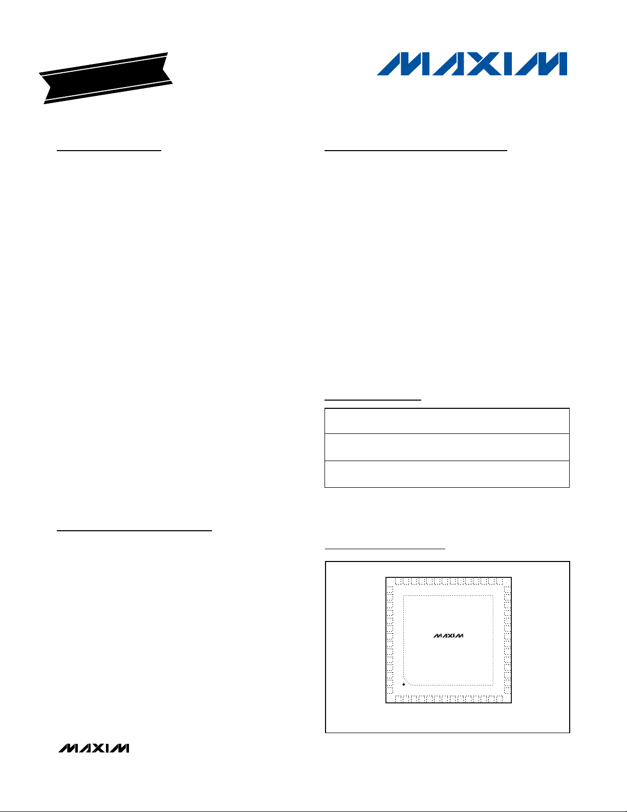
Pin Configuration
Ordering Information
19-0513; Rev 0; 5/06
For pricing, delivery, and ordering information, please contact Maxim/Dallas Direct! at
1-888-629-4642, or visit Maxim’s website at www.maxim-ic.com.
EVALUATION KIT
AVAILABLE
+
Denotes lead-free package.
D = Dry pack.
*
EP = Exposed paddle.
PART
MAX19588ETN-D
MAX19588ETN+D
RANGE
-40°C to
-40°C to
TEMP
+85°C
+85°C
PIN-PACKAGE
56 Thin QFN-EP* T5688-2
56 Thin QFN-EP* T5688-2
PKG
CODE
TOP VIEW
DD
DVDDDV
42 41 40 39 38 37 36 35 34 33 32 31 30 29
D9
43
D10
44
D11
45
D12
46
D13
47
D14
48
D15
49
DAV
50
DV
51
DD
DGND
52
53
DOR
54
N.C.
55
AV
DD
56
AV
DD
1 2 3 4 5 6 7 8 91011121314
MAX19588
EP
DDAAVDDA
CLKP
CLKN
AGND
AGND
AGND
AV
THIN QFN
8mm x 8mm
AGND
AGND
INP
DD
DGND
DGND
DV
D0D1D2D3D4D5D6D7D8
28
AGND
27
REFIN
26
REFOUT
25
AV
DD
24
AV
DD
23
AV
DD
22
AGND
21
AGND
20
AGND
19
AV
DD
18
AV
DD
17
AV
DD
16
N.C.
15
N.C.
INN
AGND
AGND
AGND
MAX19588
High-Dynamic-Range, 16-Bit,
100Msps ADC with -82dBFS Noise Floor
2 _______________________________________________________________________________________
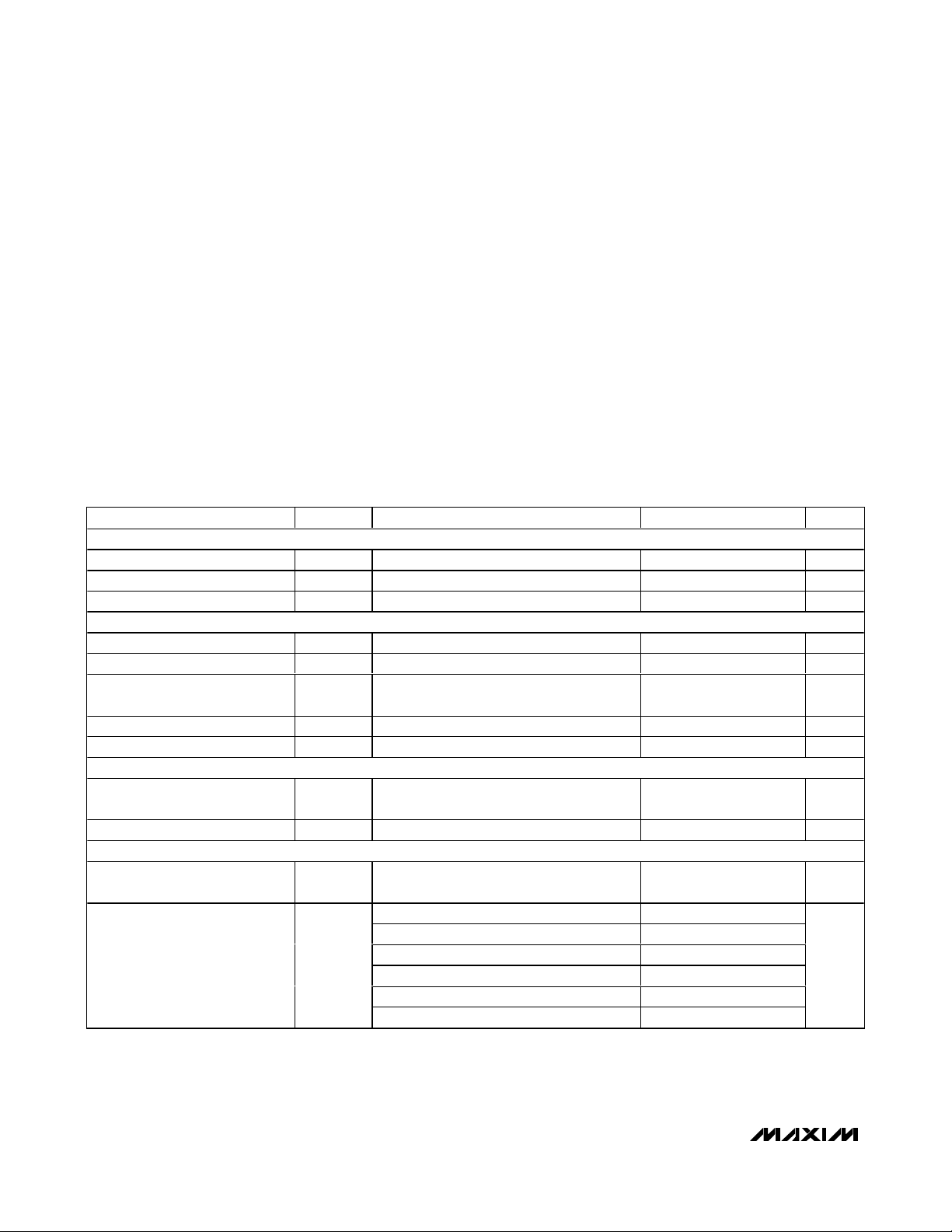
ABSOLUTE MAXIMUM RATINGS
ELECTRICAL CHARACTERISTICS
(AVDD= AV
DDA
= 3.3V, DVDD= 1.8V, AGND = DGND = 0, internal reference, INP and INN driven differentially, CLKP and CLKN driven
differentially, C
L
= 5pF at digital outputs (D0–D15, DOR), CL= 15pF for DAV, f
CLK
= 100MHz, TA= T
MIN
to T
MAX
, unless otherwise noted.
Typical values are at T
A
= +25°C, unless otherwise noted.) (Note 1)
Stresses beyond those listed under “Absolute Maximum Ratings” may cause permanent damage to the device. These are stress ratings only, and functional
operation of the device at these or any other conditions beyond those indicated in the operational sections of the specifications is not implied. Exposure to
absolute maximum rating conditions for extended periods may affect device reliability.
AVDD, AV
DDA
to AGND ........................................ -0.3V to +3.6V
DV
DD
to DGND..................................................... -0.3V to +2.4V
AGND to DGND.................................................... -0.3V to +0.3V
INP, INN, CLKP, CLKN, REFP, REFN,
REFIN, REFOUT to AGND....................-0.3V to (AV
DD
+ 0.3V)
D0–D15, DAV, DOR to GND....................-0.3V to (DV
DD
+ 0.3V)
Continuous Power Dissipation (T
A
= +70°C)
56-Pin Thin QFN-EP
(derate 47.6mW/°C above +70°C).........................3809.5mW
Operating Temperature Range ..........................-40°C to +85°C
Thermal Resistance θ
JA
..................................................21°C/W
Thermal Resistance θ
JC
.................................................0.6°C/W
Junction Temperature......................................................+150°C
Storage Temperature Range .............................-60°C to +150°C
Lead Temperature (soldering, 10s) .................................+300°C
DC ACCURACY
Resolution N 16 Bits
Offset Error V
Gain Error GE -3.5 +3.5 %FS
ANALOG INPUTS (INP, INN)
Input Voltage Range V
Common-Mode Voltage V
Differential Input Resistance R
Differential Input Capacitance C
Full-Power Analog Bandwidth BW
REFERENCE INPUT/OUTPUT (REFIN, REFOUT)
Reference Input Voltage Range REFIN
Reference Output Voltage REFOUT 1.28 V
DYNAMIC SPECIFICATIONS (f
Thermal Plus Quantization Noise
Floor
Signal-to-Noise Ratio
(First 4 Harmonics Excluded)
(Note 2)
PARAMETER SYMBOL CONDITIONS MIN TYP MAX UNITS
OS
DIFF
CM
IN
IN
-3dB
= 100Msps)
CLK
NF A
SNR
Fully differential input, VIN = V
Internally self-biased 2.4 V
-3dB rolloff for FS Input 600 MHz
< -35dBFS -82 dBFS
IN
fIN = 10MHz, AIN = -2dBFS 79.4
fIN = 70MHz, AIN = -2dBFS, TA = +25°C 77.5 79
fIN = 70MHz, AIN = -2dBFS 75.3 79
fIN = 105MHz, AIN = -2dBFS 78.3
fIN = 130MHz, AIN = -2dBFS 77.5
= 168MHz, AIN = -2dBFS 76.6
f
IN
- V
INP
01020mV
INN
2.56 V
10
±20%
7pF
1.28
±10%
P-P
kΩ
V
dB
MAX19588
High-Dynamic-Range, 16-Bit,
100Msps ADC with -82dBFS Noise Floor
_______________________________________________________________________________________ 3
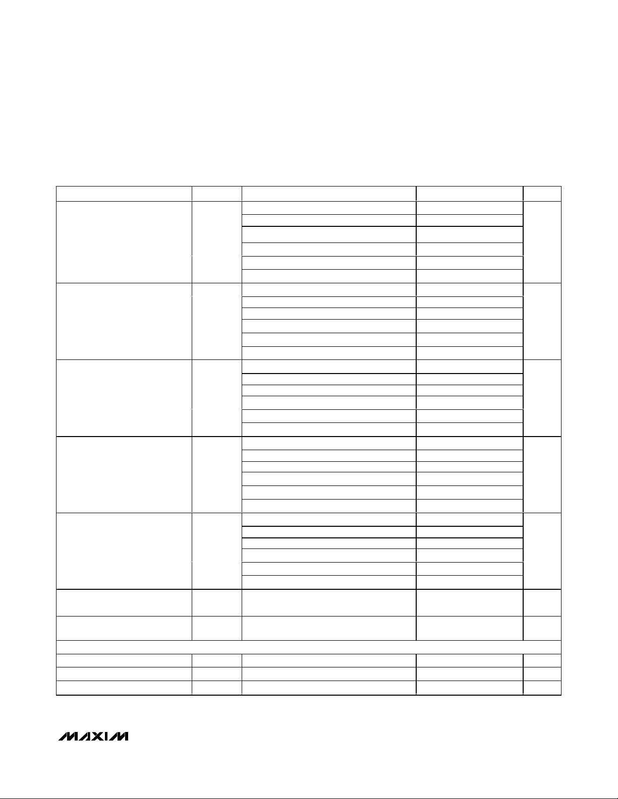
ELECTRICAL CHARACTERISTICS (continued)
(AVDD= AV
DDA
= 3.3V, DVDD= 1.8V, AGND = DGND = 0, internal reference, INP and INN driven differentially, CLKP and CLKN driven
differentially, C
L
= 5pF at digital outputs (D0–D15, DOR), CL= 15pF for DAV, f
CLK
= 100MHz, TA= T
MIN
to T
MAX
, unless otherwise noted.
Typical values are at T
A
= +25°C, unless otherwise noted.) (Note 1)
Signal-to-Noise Plus Distortion
(Note 2)
Spurious-Free Dynamic Range
(Worst Harmonic, 2nd and 3rd)
Spurious-Free Dynamic Range
(Worst Harmonic, 4th and Higher)
(Note 2)
Second-Order Harmonic
Distortion
Third-Order Harmonic Distortion HD3
Third-Order Intermodulation
Distortion
Two-Tone SFDR TTSFDR
CONVERSION RATE
Maximum Conversion Rate f
Minimum Conversion Rate f
Aperture Jitter t
PARAMETER SYMBOL CONDITIONS MIN TYP MAX UNITS
fIN = 10MHz, AIN = -2dBFS 79
fIN = 70MHz, AIN = -2dBFS, TA = +25°C 75 77.1
SINAD
SFDR1
SFDR2
HD2
IM3
CLKMAX
CLKMIN
fIN = 70MHz, AIN = -2dBFS 73.5 77.1
fIN = 105MHz, AIN = -2dBFS 77.1
fIN = 130MHz, AIN = -2dBFS 75.8
f
= 168MHz, AIN = -2dBFS 70.8
IN
fIN = 10MHz, AIN = -2dBFS 93.2
fIN = 70MHz, AIN = -2dBFS, TA = +25°C 79.6 82.1
fIN = 70MHz, AIN = -2dBFS 79.3 82.1
fIN = 105MHz, AIN = -2dBFS 86.6
fIN = 130MHz, AIN = -2dBFS 82.3
f
= 168MHz, AIN = -2dBFS 75.4
IN
fIN = 10MHz, AIN = -2dBFS 102.5
fIN = 70MHz, AIN = -2dBFS, TA = +25°C 90.4 97.7
fIN = 70MHz, AIN = -2dBFS 85 97.7
fIN = 105MHz, AIN = -2dBFS 94.2
fIN = 130MHz, AIN = -2dBFS 94.1
= 168MHz, AIN = -2dBFS 91.5
f
IN
fIN = 10MHz, AIN = -2dBFS -94.3
fIN = 70MHz, AIN = -2dBFS, TA = +25°C -93 -83
fIN = 70MHz, AIN = -2dBFS -93 -78.3
fIN = 105MHz, AIN = -2dBFS -88
fIN = 130MHz, AIN = -2dBFS -82.3
f
= 168MHz, AIN = -2dBFS -77.6
IN
fIN = 10MHz, AIN = -2dBFS -94.3
fIN = 70MHz, AIN = -2dBFS, TA = +25°C -82.1 -79.6
fIN = 70MHz, AIN = -2dBFS -82.1 -79.3
fIN = 105MHz, AIN = -2dBFS -87.4
fIN = 130MHz, AIN = -2dBFS -92.5
f
= 168MHz, AIN = -2dBFS -75.4
IN
f
= 65.1MHz, A
IN1
f
= 70.1MHz, A
IN2
f
= 65.1MHz, f
IN1
< A
< -10dBFS
IN
J
= -8dBFS
IN1
= -8dBFS
IN2
= 70.1MHz, -100dBFS
IN2
100 MHz
-87.7 dBc
98 dBFS
20 MHz
85 fs
dB
dBc
dBc
dBc
dBc
RMS
MAX19588
High-Dynamic-Range, 16-Bit,
100Msps ADC with -82dBFS Noise Floor
4 _______________________________________________________________________________________
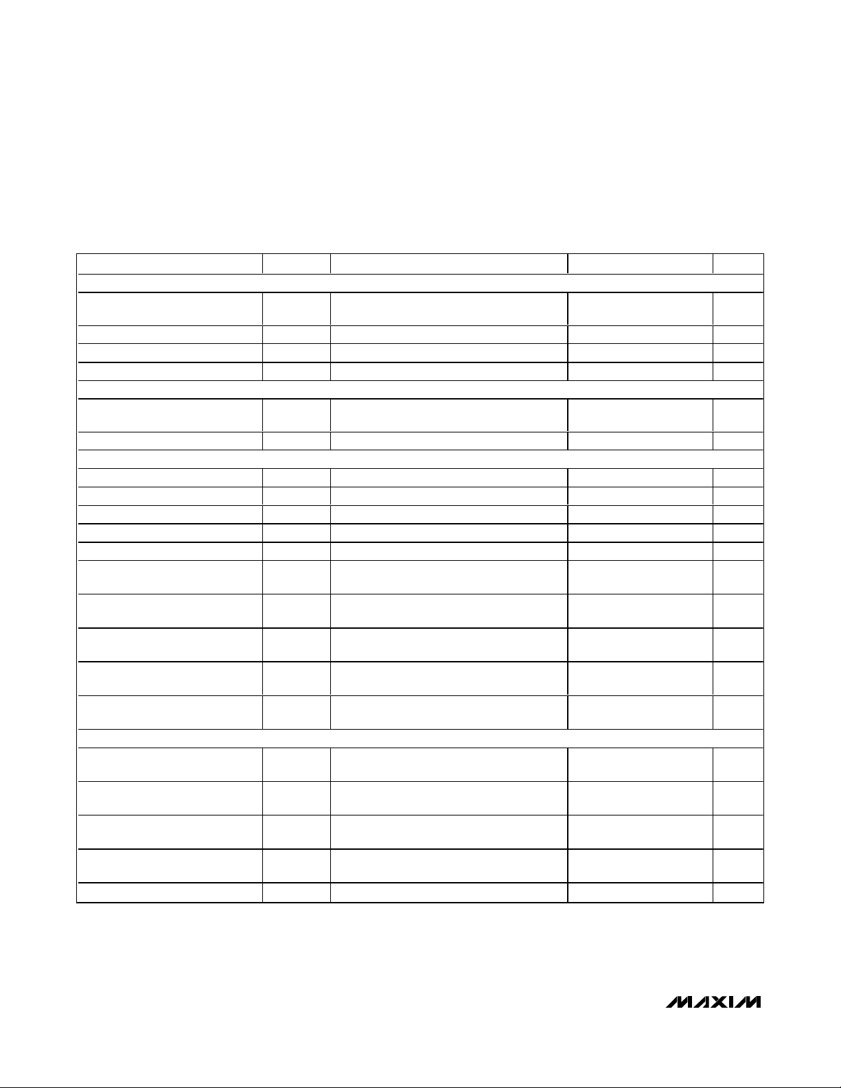
ELECTRICAL CHARACTERISTICS (continued)
(AVDD= AV
DDA
= 3.3V, DVDD= 1.8V, AGND = DGND = 0, internal reference, INP and INN driven differentially, CLKP and CLKN driven
differentially, C
L
= 5pF at digital outputs (D0–D15, DOR), CL= 15pF for DAV, f
CLK
= 100MHz, TA= T
MIN
to T
MAX
, unless otherwise noted.
Typical values are at T
A
= +25°C, unless otherwise noted.) (Note 1)
Note 1: TA≥ +25°C guaranteed by production test, TA< +25°C guaranteed by design and characterization. Typical values are at TA=
+25°C.
Note 2: AC parameter measured in a 32,768-point FFT record, where the first 2 bins of the FFT and 2 bins on either side of the carrier
are excluded. For SNR and SINAD measurements, bins dominated by production test system noise are excluded.
Note 3: Parameter guaranteed by design and characterization.
CLOCK INPUTS (CLKP, CLKN)
Differential Input Swing V
Common-Mode Voltage V
Differential Input Resistance R
Differential Input Capacitance C
CMOS-COMPATIBLE DIGITAL OUTPUTS (D0–D15, DOR, DAV)
Digital Output High Voltage V
Digital Output Low Voltage V
TIMING SPECIFICATIONS (Figures 4, 5), CL = 7.5pF (D0–D15, DOR); CL = 35pF (DAV)
CLKP - CLKN High t
CLKP - CLKN Low t
Effective Aperture Delay t
Output Data Delay t
Data Valid Delay t
Pipeline Latency t
CLKP Rising Edge to DATA Not
Valid
CLKP Rising Edge to DATA
Guaranteed Valid
DATA Setup Time Before Rising
DAV
DATA Hold Time After Rising
DAV
POWER SUPPLIES
Analog Power-Supply Voltage
Digital Output Power-Supply
Voltage
Analog Power-Supply Current
Digital Output Power-Supply
Current
Power Dissipation P
PARAMETER SYMBOL CONDITIONS MIN TYP MAX UNITS
DIFFCLK
CMCLK
INCLK
INCLK
OH
OL
CLKP
CLKN
AD
DAT
DAV
LATENCY
t
DNV
t
DGV
t
t
H
AV
A
VDDA
DV
I
AVDD
I
AVDDA
I
DVDD
DISS
Fully differential inputs
Self-biased 1.6 V
DV
I
I
= 200µA
SOURCE
= 200µA 0.2 V
SINK
DD
0.2
(Note 3) 4 ns
(Note 3) 4 ns
(Note 3) 2.5 4 5.2 ns
(Note 3) 1.1 ns
(Note 3) 7.5 ns
Clock duty cycle = 50% (Note 3) 2 ns
S
Clock duty cycle = 50% (Note 3) 2.5 ns
,
DD
DD
3.13 3.3 3.46 V
1.7 1.8 1.9 V
+
1.0 to
5.0
V
P-P
10 kΩ
3pF
V
-300 ps
3.4 ns
7
Clock
Cycles
369 450 mA
31 42 mA
1275 1561 mW
MAX19588
High-Dynamic-Range, 16-Bit,
100Msps ADC with -82dBFS Noise Floor
_______________________________________________________________________________________
5
Typical Operating Characteristics
(AVDD= AV
DDA =
3.3V, DVDD= 1.8V, INP and INN driven differentially, internal reference, CLKP and CLKN driven differentially, CL=
7.5pF at digital outputs (D0–D15, DOR), C
L
= 35pF for DAV, f
CLK
= 100MHz, TA= +25°C. Unless otherwise noted, all AC data based
on 32k-point FFT records.)
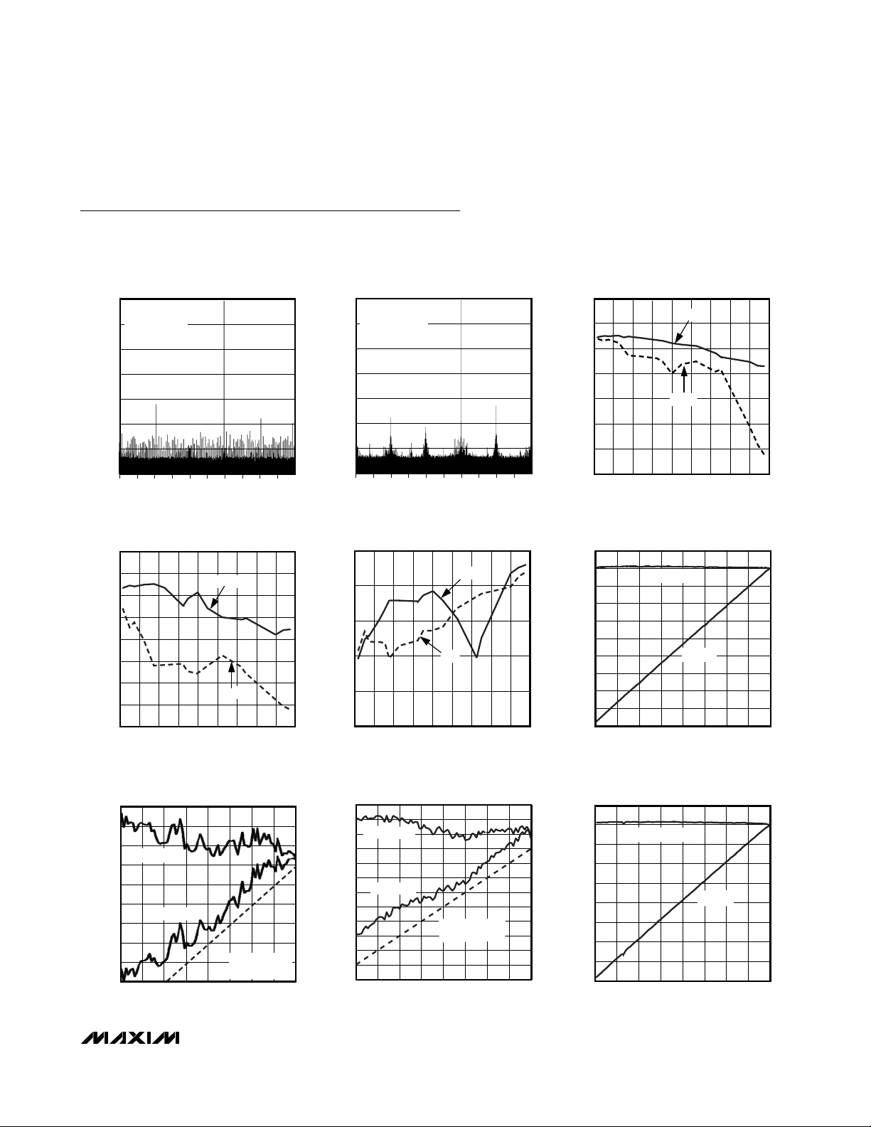
FFT PLOT
(524,288-POINT DATA RECORD)
0
f
= 100MHz
CLK
= 70.164MHz
f
IN
-20
= -1.94dBFS
A
IN
-40
-60
-80
AMPLITUDE (dBFS)
-100
-120
-140
3
0105 152025 35 4530 40
ANALOG INPUT FREQUENCY (MHz)
2
SFDR1/SFDR2 vs. ANALOG INPUT FREQUENCY
= 100MHz, AIN = -2dBFS)
(f
110
105
100
95
90
85
SFDR1/SFDR2 (dBc)
80
75
70
CLK
SFDR2
SFDR1
0 40608020 100 120 140 160 180
fIN (MHz)
0
f
CLK
f
IN
-20
A
MAX19588 toc01
IN
-40
-60
-80
AMPLITUDE (dBFS)
-100
-120
-140
0105 152025 35 45
HD2/HD3 vs. ANALOG INPUT FREQUENCY
-70
MAX19588toc04
-80
-90
-100
HD2/HD3 (dBc)
-110
-120
0 40608020 100 120 140 160 180
(524,288-POINT DATA RECORD)
= 100MHz
= 130.001MHz
= -1.98dBFS
(f
FFT PLOT
3
30 40
ANALOG INPUT FREQUENCY (MHz)
= 100MHz, AIN = -2dBFS)
CLK
HD3
HD2
fIN (MHz)
SNR/SINAD vs. ANALOG INPUT FREQUENCY
82
80
MAX19588 toc02
78
76
MAX19588toc05
74
SNR/SINAD (dB)
72
70
68
04020 60 80 100 120 140 160 180
90
80
70
60
50
40
SNR (dB, dBFS)
30
20
10
0
-80 -60 -50 -40-70 -30 -20 -10 0
2
= 100MHz, AIN = -2dBFS)
(f
CLK
SNR
SINAD
fIN (MHz)
SNR vs. ANALOG INPUT AMPLITUDE
= 100MHz, fIN = 10MHz)
(f
CLK
SNR (dBFS)
SNR (dB)
ANALOG INPUT AMPLITUDE (dBFS)
MAX19588 toc03
MAX19588toc06
SFDR1 vs. ANALOG INPUT AMPLITUDE
= 100MHz, fIN = 10MHz)
(f
120
110
100
90
80
70
SFDR1 (dBc, dBFS)
60
50
40
30
CLK
SFDR1 (dBFS)
SFDR1 (dBc)
SFDR = 90dB
REFERENCE LINE
-80 -60 -50 -40-70 -30 -20 -10 0
ANALOG INPUT AMPLITUDE (dBFS)
MAX19588toc07
SFDR2 (dBc, dBFS)
SFDR2 vs. ANALOG INPUT AMPLITUDE
= 100MHz, fIN = 10MHz)
(f
120
110
100
90
80
70
60
50
40
30
20
10
CLK
SFDR2 (dBFS)
SFDR2 (dBc)
SFDR = 90dB
REFERENCE LINE
0
-80 -60 -50 -40-70 -30 -20 -10 0
ANALOG INPUT AMPLITUDE (dBFS)
MAX19588toc08
SNR vs. ANALOG INPUT AMPLITUDE
= 100MHz, fIN = 70MHz)
(f
90
80
70
60
50
40
SNR (dB, dBFS)
30
20
10
CLK
SNR (dBFS)
SNR (dB)
0
-80 -60 -50 -40-70 -30 -20 -10 0
ANALOG INPUT AMPLITUDE (dBFS)
MAX19588toc09
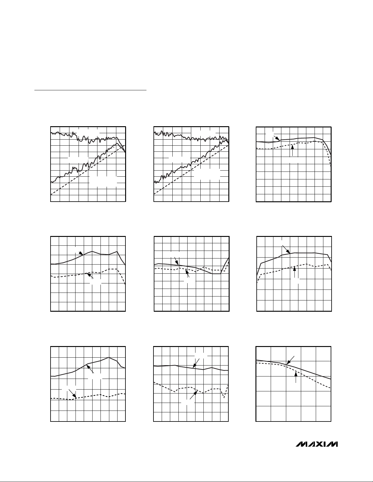
Typical Operating Characteristics (continued)
(AVDD= AV
DDA =
3.3V, DVDD= 1.8V, INP and INN driven differentially, internal reference, CLKP and CLKN driven differentially, CL=
7.5pF at digital outputs (D0–D15, DOR), C
L
= 35pF for DAV, f
CLK
= 100MHz, TA= +25°C. Unless otherwise noted, all AC data based
on 32k-point FFT records.)
70
80
95
75
85
100
90
105
20 40 50 6030 70 80 90 100 110
SFDR1/SFDR2 vs. SAMPLING FREQUENCY
(f
IN
= 70MHz, AIN = -2dBFS)
MAX19588toc16
f
CLK
(MHz)
SFDR/SFDR2 (dB)
SFDR2
SFDR1
-110
-100
-90
-105
-95
-70
20 40 50 6030 70 80 90 100 110
HD2/HD3 vs. SAMPLING FREQUENCY
(f
IN
= 70MHz, AIN = -2dBFS)
MAX19588toc17
f
CLK
(MHz)
HD2/HD3 (dBc)
-80
-85
-75
HD3
HD2
72
74
76
82
-40 -15 10 35 60 85
SNR/SINAD vs. TEMPERATURE
(f
CLK
= 100MHz, fIN = 10.1MHz, AIN = -2dBFS)
MAX19588toc18
TEMPERATURE (°C)
SNR/SINAD (dB)
78
80
SNR
SINAD
MAX19588
High-Dynamic-Range, 16-Bit,
100Msps ADC with -82dBFS Noise Floor
6 _______________________________________________________________________________________
SFDR1 vs. ANALOG INPUT AMPLITUDE
120
110
100
90
80
70
60
50
SFDR1 (dBc, dBFS)
40
30
20
10
0
-80 -60 -50 -40-70 -30 -20 -10 0
= 100MHz, fIN = 70MHz)
(f
CLK
SFDR1 (dBFS)
SFDR1 (dBc)
SFDR = 90dB
REFERENCE LINE
ANALOG INPUT AMPLITUDE (dBFS)
SFDR2 vs. ANALOG INPUT AMPLITUDE
120
110
100
MAX19588toc10
90
80
70
60
50
40
SFDR2 (dBc, dBFS)
30
20
10
0
-80 -60 -50 -40-70 -30 -20 -10 0
SNR/SINAD vs. SAMPLING FREQUENCY
= 100MHz, fIN = 70MHz)
(f
CLK
SFDR2 (dBFS)
SFDR2 (dBc)
SFDR = 90dB
REFERENCE LINE
ANALOG INPUT AMPLITUDE (dBFS)
MAX19588toc11
81
80
79
78
77
76
75
SNR/SINAD (dB)
74
73
72
71
20 40 50 6030 70 80 90 100 110
= 10MHz, AIN = -2dBFS)
(f
IN
SNR
SINAD
f
(MHz)
CLK
MAX19588toc12
SFDR1/SFDR2 vs. SAMPLING FREQUENCY
= 10MHz, AIN = -2dBFS)
(f
110
105
100
95
90
85
SFDR1/SFDR2 (dBc)
80
75
70
IN
SFDR2
20 30 40 50 60 70 80 90 100 110
HD2/HD3 vs. SAMPLING FREQUENCY
= 10MHz, AIN = -2dBFS)
(f
-70
-75
MAX19588toc13
-80
-85
-90
-95
SFDR1
f
(MHz)
CLK
-100
HD2/HD3 (dBc)
-105
-110
-115
-120
IN
HD3
HD2
20 30 40 50 60 70 80 90 100 110
f
(MHz)
CLK
MAX19588toc14
SNR/SINAD vs. SAMPLING FREQUENCY
= 70MHz, AIN = -2dBFS)
(f
82
80
78
76
74
SNR/SINAD (dB)
72
70
68
IN
SNR
SINAD
20 30 40 50 60 70 80 90 100 110
f
(MHz)
CLK
MAX19588toc15
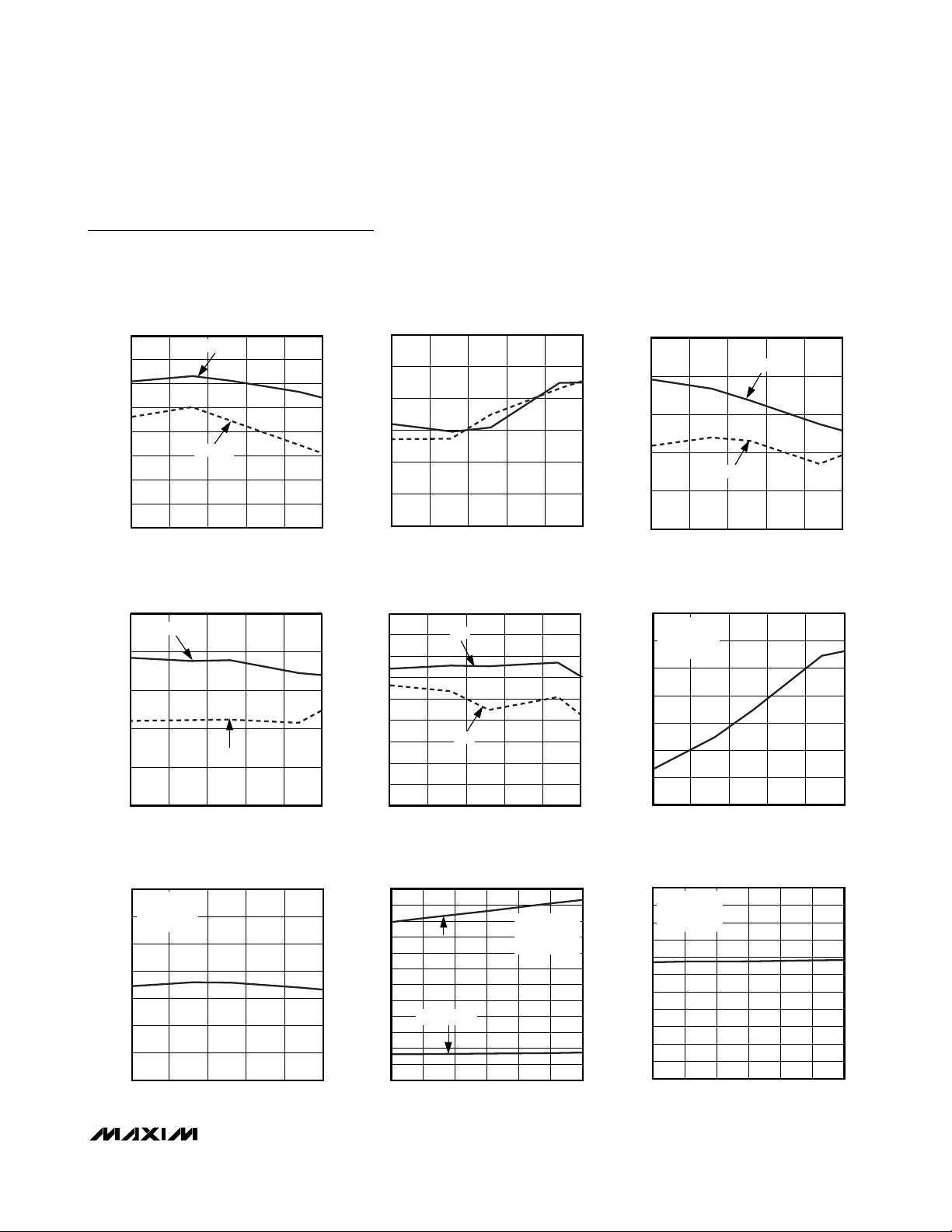
Typical Operating Characteristics (continued)
(AVDD= AV
DDA =
3.3V, DVDD= 1.8V, INP and INN driven differentially, internal reference, CLKP and CLKN driven differentially, CL=
7.5pF at digital outputs (D0–D15, DOR), C
L
= 35pF for DAV, f
CLK
= 100MHz, TA= +25°C. Unless otherwise noted, all AC data based
on 32k-point FFT records.)
MAX19588
High-Dynamic-Range, 16-Bit,
100Msps ADC with -82dBFS Noise Floor
_______________________________________________________________________________________
7
SNR/SINAD
(dB)
HD2/HD3
(dB
)
REFERENCE
VOLTAGE
(V)
SFDR1/SFDR2 vs. TEMPERATURE
= 100MHz, fIN = 10.1MHz, AIN = -2dBFS)
(f
CLK
110
105
100
95
90
85
SFDR1/SFDR2 (dBc)
80
75
70
-40 -15 10 35 60 85
SFDR2
SFDR1
TEMPERATURE (°C)
SFDR1/SFDR2 vs. TEMPERATURE
= 100MHz, fIN = 70.1MHz, AIN = -2dBFS)
(f
CLK
110
SFDR2
100
90
80
SFDR1/SFDR2 (dBc)
70
60
-40 -15 10 35 60 85
SFDR1
TEMPERATURE (°C)
REFERENCE VOLTAGE
vs. TEMPERTURE
1.31
f
= 100MHz
CLK
= 70.1MHz
f
IN
1.30
1.29
1.28
1.27
1.26
REFERENCE VOLTAGE (V)
1.25
1.24
= -2dBFS
A
IN
-40 -15 10 35 60 85
TEMPERATURE (°C)
= 100MHz, fIN = 10.1MHz, AIN = -2dBFS)
(f
CLK
-80
-85
MAX19588toc19
-90
-95
HD2/HD3 (dBc)
-100
-105
-110
-40 -15 10 35 60 85
= 100MHz, fIN = 70.1MHz, AIN = -2dBFS)
(f
CLK
-70
-75
MAX19588toc22
-80
-85
c
-90
-95
-100
-105
-110
-115
-40 -15 10 35 60 85
1400
1300
1200
MAX19588toc25
1100
1000
(mA, mW)
900
DISS
800
, P
700
AVDDA
600
+ I
500
AVDD
I
400
300
200
3.15 3.20 3.25 3.30 3.35 3.40 3.45
HD2/HD3 vs. TEMPERATURE
vs. ANALOG SUPPLY VOLTAGE
HD2/HD3 vs. TEMPERATURE
HD2
HD3
TEMPERATURE (°C)
MAX19588toc20
SNR/SINAD vs. TEMPERATURE
= 100MHz, fIN = 70.1MHz, AIN = -2dBFS)
(f
CLK
82
80
78
76
74
72
-40-1510356085
TEMPERATURE (°C)
SNR
SINAD
POWER DISSIPATION
vs. TEMPERATURE
1300
f
= 100MHz
HD3
MAX19588toc23
HD2
TEMPERATURE (°C)
POWER DISSIPTATION
CLK
= 70.1MHz
f
IN
1290
= -2dBFS
A
IN
1280
1270
1260
1250
POWER DISSIPATION (mW)
1240
1230
-40 -15 10 35 60 85
TEMPERATURE (°C)
REFERENCE VOLTAGE
vs. ANALOG SUPPLY VOLTAGE
1.280
f
= 100MHz
CLK
P
DISS
I
AVDD + IAVDDA
ANALOG SUPPLY VOLTAGE (V)
f
= 100MHz
CLK
= 70.1MHz
f
IN
= -2dBFS
A
IN
MAX19588toc26
1.279
1.278
1.277
1.276
1.275
1.274
1.273
1.272
1.271
1.270
= 70.1MHz
f
IN
= -2dBFS
A
IN
3.15 3.20 3.25 3.30 3.35 3.40 3.45
ANALOG SUPPLY VOLTAGE (V)
MAX19588toc21
MAX19588toc24
MAX19588toc27

Typical Operating Characteristics (continued)
(AVDD= AV
DDA =
3.3V, DVDD= 1.8V, INP and INN driven differentially, internal reference, CLKP and CLKN driven differentially, CL=
7.5pF at digital outputs (D0–D15, DOR), C
L
= 35pF for DAV, f
CLK
= 100MHz, TA= +25°C. Unless otherwise noted, all AC data based
on 32k-point FFT records.)
MAX19588
High-Dynamic-Range, 16-Bit,
100Msps ADC with -82dBFS Noise Floor
8 _______________________________________________________________________________________
81
f
80
f
A
79
78
77
76
SNR/SINAD (dB)
75
74
73
3.15 3.20 3.25 3.30 3.35 3.40 3.45
SNR/SINAD
vs. ANALOG SUPPLY VOLTAGE
= 100MHz
CLK
= 70.1MHz
IN
= -2dBFS
IN
SNR
SINAD
ANALOG SUPPLY VOLTAGE (V)
0
-20
-40
-60
AMPLITUDE (dBFS)
-80
-100
f
IN1
vs. ANALOG SUPPLY VOLTAGE
110
f
= 100MHz
CLK
105
= 70.1MHz
f
MAX19588toc28
SFDR1/SFDR2 (dBc)
IN
= -2dBFS
A
IN
100
95
90
85
80
75
70
3.15 3.20 3.25 3.30 3.35 3.40 3.45
ANALOG SUPPLY VOLTAGE (V)
TWO-TONE SFDR PLOT
(32,786-POINT DATA RECORD)
f
= 100MHz
CLK
= 10.098MHz
f
IN1
= -7.95dBFS
A
IN1
= 14.871MHz
f
IN2
= -8.01dBFS
A
IN2
IM3 = -104.1dBc
f
IN2
f
- f
IN2
IN1
2f
- f
IN2
IN1
SFDR1/SFDR2
-70
f
CLK
-75
= 70.1MHz
f
MAX19588toc29
SFDR2
HD2/HD3 (dBc)
SFDR1
IN
A
IN
-80
-85
-90
-95
-100
-105
-110
3.15 3.20 3.25 3.30 3.35 3.40 3.45
TWO-TONE SFDR PLOT
(32,786-POINT DATA RECORD)
0
f
= 100MHz
CLK
= 70.102MHz
f
IN1
-20
= -8.03dBFS
A
MAX19588 toc31
IN
= 65.097MHz
f
IN2
= -8.13dBFS
A
IN2
-40
IM3 = -87.7dBc
-60
AMPLITUDE (dBFS)
-80
-100
f
IN1
2f
- f
IN1
IN2
vs. ANALOG SUPPLY VOLTAGE
HD2/HD3
= 100MHz
= -2dBFS
HD3
HD2
ANALOG SUPPLY VOLTAGE (V)
MAX19588 toc32
f
IN2
2f
- f
IN2
IN1
MAX19588toc30
-120
0105 152025 35 4530 40 50
ANALOG INPUT FREQUENCY (MHz)
TWO-TONE SFDR vs. ANALOG INPUT
AMPLITUDE (f
= 10.1MHz, f
f
IN1
120
110
100
TTSFDR (dBFS)
90
80
70
60
50
TTSFDR (dBc)
40
TTSFDR (dBc, dBFS)
30
20
10
0
-100 -80 -70 -60-90 -50 -40 -30 -20 -10 0
ANALOG INPUT AMPLITUDE (dBFS)
= 100MHz,
CLK
= 15.1MHz)
IN2
TTSFDR = 90dB
REFERENCE LINE
MAX19588toc33
-120
0105 152025 35 4530 40 50
ANALOG INPUT FREQUENCY (MHz)
TWO-TONE SFDR vs. ANALOG INPUT
AMPLITUDE (f
= 65.1MHz, f
f
IN1
120
110
100
TTSFDR (dBFS)
90
80
70
60
50
TTSFDR (dBc)
40
TTSFDR (dBc, dBFS)
30
20
10
0
-100 -80 -70 -60-90 -50 -40 -30 -20 -10 0
ANALOG INPUT AMPLITUDE (dBFS)
= 100MHz,
CLK
= 70.1MHz)
IN2
TTSFDR = 90dB
REFERENCE LINE
MAX19588toc34

MAX19588
High-Dynamic-Range, 16-Bit,
100Msps ADC with -82dBFS Noise Floor
_______________________________________________________________________________________ 9
Pin Description
PIN NAME FUNCTION
1, 2 AV
3, 6–9, 12,
13, 14, 20,
21, 22, 28
4 CLKP Differential Clock, Positive Input Terminal
5 CLKN Differential Clock, Negative Input Terminal
10 INP Differential Analog Input, Positive Terminal
11 INN Differential Analog Input, Negative Terminal
15, 16, 54 N.C. No Connection. Do not connect to this pin.
17, 18, 19,
23, 24, 25,
55, 56
26 REFOUT Internal Bandgap Reference Output
27 REFIN Reference Voltage Input
29, 41, 42, 51 DV
30, 31, 52 DGND Converter Ground. Digital output-driver ground.
32 D0 Digital CMOS Output Bit 0 (LSB)
33 D1 Digital CMOS Output Bit 1
34 D2 Digital CMOS Output Bit 2
35 D3 Digital CMOS Output Bit 3
36 D4 Digital CMOS Output Bit 4
37 D5 Digital CMOS Output Bit 5
38 D6 Digital CMOS Output Bit 6
39 D7 Digital CMOS Output Bit 7
40 D8 Digital CMOS Output Bit 8
43 D9 Digital CMOS Output Bit 9
44 D10 Digital CMOS Output Bit 10
45 D11 Digital CMOS Output Bit 11
46 D12 Digital CMOS Output Bit 12
47 D13 Digital CMOS Output Bit 13
48 D14 Digital CMOS Output Bit 14
49 D15 Digital CMOS Output Bit 15 (MSB)
50 DAV
DDA
AGND
AV
DD
DD
Auxiliary Analog Supply Voltage. Connect these pins together and connect to AVDD through a 50Ω
series resistor.
Converter Ground. Analog, digital, and output-driver grounds are internally connected to the same
potential. Connect the converter’s exposed paddle (EP) to GND.
Analog Supply Voltage. Provide local bypassing to ground with 0.01µF and 0.1µF capacitors.
Digital Supply Voltage. Provide local bypassing to ground with 0.01µF and 0.1µF capacitors.
Data Valid Output. This output can be used as a clock control line to drive an external buffer or dataacquisition system. The typical delay time between the falling edge of the converter clock and the
rising edge of DAV is 4ns.
Data Over-Range Bit. This control line flags an over-/under-range condition in the ADC. If DOR
53 DOR
— EP Exposed Paddle. Must be connected to AGND.
transitions high, an over-/under-range condition was detected. If DOR remains low, the ADC operates
within the allowable full-scale range.

MAX19588
High-Dynamic-Range, 16-Bit,
100Msps ADC with -82dBFS Noise Floor
10 ______________________________________________________________________________________
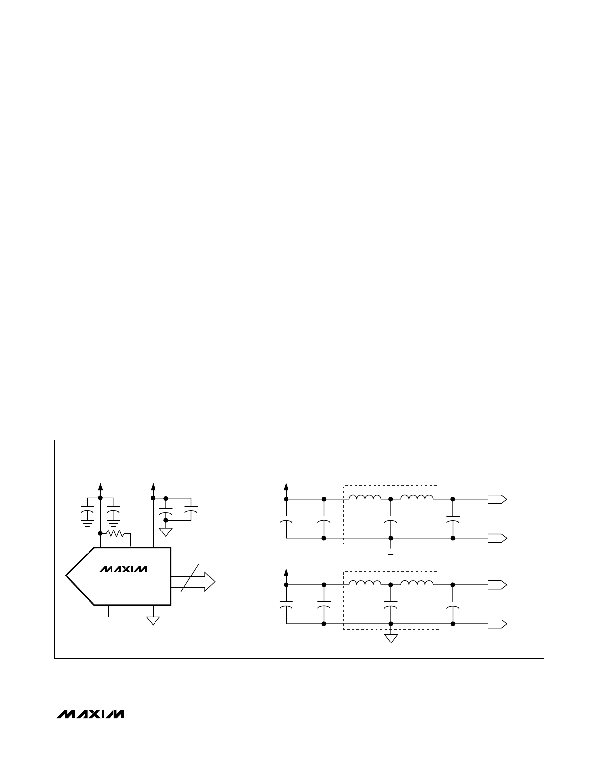
Detailed Description
Figure 1 provides an overview of the MAX19588 architecture. The MAX19588 employs an input track-andhold (T/H) amplifier, which has been optimized for low
thermal noise and low distortion. The high-impedance
differential inputs to the T/H amplifier (INP and INN) are
self-biased at approximately 2.4V, and support a fullscale 2.56V
P-P
differential input voltage. The output of
the T/H amplifier is applied to a multistage pipelined
ADC core, which is designed to achieve a very low
thermal noise floor and low distortion.
A clock buffer receives a differential input clock waveform and generates a low-jitter clock signal for the input
T/H. The signal at the analog inputs is sampled at the
rising edge of the differential clock waveform. The differential clock inputs (CLKP and CLKN) are highimpedance inputs, are self-biased at 1.6V, and support
differential clock waveforms from 1V
P-P
to 5V
P-P
.
The outputs from the multistage pipelined ADC core
are delivered to error correction and formatting logic,
which deliver the 16-bit output code in two’s-complement format to digital output drivers. The output drivers
provide 1.8V CMOS-compatible outputs.
Analog Inputs (INP, INN)
The signal inputs to the MAX19588 (INP and INN) are balanced differential inputs. This differential configuration
provides immunity to common-mode noise coupling and
rejection of even-order harmonic terms. The differential
signal inputs to the MAX19588 should be AC-coupled
and carefully balanced to achieve the best dynamic performance (see
Differential, AC-Coupled Analog Inputs
in
the
Applications Information
section for more details). ACcoupling of the input signal is required because the
MAX19588 inputs are self-biasing as shown in Figure 2.
Although the track-and-hold inputs are high impedance,
the actual differential input impedance is nominally 10kΩ
because of the two 5kΩ resistors connected to the
common-mode bias circuitry.
Avoid injecting any DC leakage currents into these analog inputs. Exceeding a DC leakage current of 10µA
shifts the self-biased common-mode level, adversely
affecting the converter’s performance.
On-Chip Reference Circuit
The MAX19588 incorporates an on-chip 1.28V, low-drift
bandgap reference. This reference potential establishes the full-scale range for the converter, which is nominally 2.56V
P-P
differential (Figure 3). The internal
reference voltage can be monitored by REFOUT.
To use the internal reference voltage the reference
input (REFIN) must be connected to REFOUT
through a 10kΩ resistor. Bypass both pins with sepa-
rate 1µF capacitors to AGND.
The MAX19588 also allows an external reference
source to be connected to REFIN, enabling the user to
overdrive the internal bandgap reference. REFIN
accepts a 1.28V ±10% input voltage range.
Figure 1. Block Diagram
CLKP
CLKN
INP
INN
CLOCK
BUFFER
T/H
MAX19588
PIPELINE
ADC
REFERENCE
REFOUT REFIN
CMOS
DRIVER
CMOS
OUTPUT
DRIVERS
16
AV
DD
AGND
DV
DD
DAV
DOR
D0–D15
DGND

MAX19588
High-Dynamic-Range, 16-Bit,
100Msps ADC with -82dBFS Noise Floor
______________________________________________________________________________________ 11
Clock Inputs (CLKP, CLKN)
The differential clock buffer for the MAX19588 has been
designed to accept an AC-coupled clock waveform.
Like the signal inputs, the clock inputs are self-biasing.
In this case, the self-biased potential is 1.6V and each
input is connected to the reference potential with a 5kΩ
resistor. Consequently, the differential input resistance
associated with the clock inputs is 10kΩ. While differential clock signals as low as 0.5V
P-P
can be used to
drive the clock inputs, best dynamic performance is
achieved with 1V
P-P
to 5V
P-P
clock input voltage levels.
Jitter on the clock signal translates directly to jitter
(noise) on the sampled signal. Therefore, the clock
source must be a very low-jitter (low-phase-noise)
source. Additionally, extremely low phase-noise oscillators and bandpass filters should be used to obtain the
true AC performance of this converter. See the
Differential, AC-Coupled Clock Inputs
and
Testing the
MAX19588
topics in the
Applications Information
section for additional details on the subject of driving the
clock inputs.
System Timing Requirements
Figure 4 depicts the general timing relationships for the
signal input, clock input, data output, and DAV output.
Figure 5 shows the detailed timing specifications and
signal relationships, as defined in the
Electrical
Characteristics
table.
The MAX19588 samples the input signal on the rising
edge of the input clock. Output data is valid on the rising edge of the DAV signal, with a 7 clock-cycle data
latency. Note that the clock duty cycle should typically
be 50% ±10% for proper operation.
Digital Outputs (D0–D15, DAV, DOR)
For best performance, the capacitive loading on the
digital outputs of the MAX19588 should be kept as low
as possible (< 10pF). Due to the current-limited dataoutput driver of the MAX19588, large capacitive loads
increase the rise and fall time of the data and can make
it more difficult to register the data into the next IC. The
loading capacitance can be kept low by keeping the
output traces short and by driving a single CMOS
buffer or latch input (as opposed to multiple CMOS
inputs). The output data is in two’s-complement format,
as illustrated in Table 1.
Data is valid at the rising edge of DAV (Figures 4, 5).
DAV may be used as a clock signal to latch the output
data. Note that the DAV output driver is not current limited, hence it allows for higher capacitive loading.
The converter’s DOR output signal is used to identify
over- and under-range conditions. If the input signal
exceeds the positive or negative full-scale range for the
MAX19588 then DOR will be asserted high. The timing
for DOR is identical to the timing for the data outputs,
and DOR therefore provides an over-range indication
on a sample-by-sample basis.
Figure 2. Simplified Analog Input Architecture
Figure 3. Full-Scale Voltage Range
T/H AMPLIFIER
INP
5kΩ
OTA
5kΩ
INN
T/H AMPLIFIER
TO FIRST QUANTIZER
STAGE
TO FIRST QUANTIZER
STAGE
2.56V
P-P
DIFFERENTIAL FSR
INP
INN
-640mV
+640mV
COMMON-MODE
VOLTAGE (2.4V)

MAX19588
High-Dynamic-Range, 16-Bit,
100Msps ADC with -82dBFS Noise Floor
12 ______________________________________________________________________________________
Figure 4. General System Output Timing Diagram
Figure 5. Detailed Timing Information for Clock Operation
N + 1
N
ANALOG INPUT
CLOCK INPUT
D0–D15
DAV
INP
INN
CLKN
CLKP
D0–D15
DOR
N - 7
N N + 1 N + 2 N + 3
t
DAT
N - 7
t
DAV
N - 6
7 CLOCK-CYCLE LATENCY (t
N + 2
N + 3
N - 5 N - 4 N - 3 N - 2 N - 1 N
t
AD
t
DNV
N - 6
t
DGV
LATENCY
t
CLKP
)
N + 4
t
N + 5
t
CLKN
N - 5
S
t
H
N + 6
N - 4
N + 7
DAV
: DELAY FROM CLKN TO DATA VALID CLOCK DAV
ENCODE AT CLKP - CLKN > 0 (RISING EDGE)
: CLKP - CLKN > 0
t
CLKP
: CLKP - CLKN < 0
t
CLKN
: EFFECTIVE APERTURE DELAY
t
AD
: DELAY FROM CLKP TO OUTPUT DATA TRANSITION
t
DAT
t
DAV
: CLKP RISING EDGE TO DATA NOT VALID
t
DNV
: CLKP RISING EDGE TO DATA GUARANTEED VALID
t
DGV
: DATA SETUP TIME BEFORE RISING DAV
t
S
: DATA HOLD TIME AFTER RISING DAV
t
H

MAX19588
High-Dynamic-Range, 16-Bit,
100Msps ADC with -82dBFS Noise Floor
______________________________________________________________________________________ 13
Applications Information
Differential, AC-Coupled Clock Inputs
The clock inputs to the MAX19588 are driven with an
AC-coupled differential signal, and best performance is
achieved under these conditions. However, it is often
the case that the available clock source is single-ended.
Figure 6 demonstrates one method for converting a single-ended clock signal into a differential signal with a
transformer. In this example, the transformer turns ratio
from the primary to secondary side is 1:1.414. The
impedance ratio from primary to secondary is the
square of the turns ratio, or 1:2. So terminating the sec-
ondary side with a 100Ω differential resistance results in
a 50Ω load looking into the primary side of the transformer. The termination resistor in this example is composed of the series combination of two 50Ω resistors
with their common node AC-coupled to ground.
Figure 6 illustrates the secondary side of the transformer to be coupled directly to the clock inputs. Since
the clock inputs are self-biasing, the center tap of the
transformer must be AC-coupled to ground or left floating. If the center tap of the transformer’s secondary
side is DC-coupled to ground, it is necessary to add
blocking capacitors in series with the clock inputs.
Table 1. MAX19588 Digital Output Coding
Figure 6. Transformer-Coupled Clock Input Configuration
INP
ANALOG VOLTAGE LEVEL
VCM + 0.64V VCM - 0.64V
V
CM
VCM - 0.64V VCM + 0.64V
ANALOG VOLTAGE LEVEL
INN
V
CM
TWO’S-COMPLEMENT CODE
0 1 1 1 1 1 1 1 1 1 1 1 1 1 1 1
0 0 0 0 0 0 0 0 0 0 0 0 0 0 0 0
1 1 1 1 1 1 1 1 1 1 1 1 1 1 1 1
1 0 0 0 0 0 0 0 0 0 0 0 0 0 0 0
D15–D0
(positive full-scale)
(midscale + δ)
(midscale - δ)
(negative full-scale)
AV
DDDVDD
0.1μF
T2-1T-KK81
49.9Ω
49.9Ω
BACK-TO-BACK DIODE
0.1μF
INP
INN
MAX19588
CLKP CLKN
AGND
D0–D15
16
DGND

MAX19588
High-Dynamic-Range, 16-Bit,
100Msps ADC with -82dBFS Noise Floor
14 ______________________________________________________________________________________
Clock jitter is generally improved if the clock signal has
a high slew rate at the time of its zero-crossing.
Therefore, if a sinusoidal source is used to drive the
clock inputs, the clock amplitude should be as large as
possible to maximize the zero-crossing slew rate. The
back-to-back Schottky diodes shown in Figure 6 are not
required as long as the input signal is held to a differential voltage potential of 3V
P-P
or less. If a larger amplitude signal is provided (to maximize the zero-crossing
slew rate), then the diodes serve to limit the differential
signal swing at the clock inputs. Note that all AC specifications for the MAX19588 are measured within this
configuration and with an input clock amplitude of
approximately 12dBm.
Any differential mode noise coupled to the clock inputs
translates to clock jitter and degrades the SNR performance of the MAX19588. Any differential mode coupling
of the analog input signal into the clock inputs results in
harmonic distortion. Consequently, it is important that the
clock lines be well isolated from the analog signal input
and from the digital outputs. See the
Signal Routing
sec-
tion for more discussion on the subject of noise coupling.
Differential, AC-Coupled Analog Inputs
The analog inputs INP and INN are driven with a differential AC-coupled signal. It is important that these
inputs be accurately balanced. Any common-mode signal applied to these inputs degrades even-order distortion terms. Therefore, any attempt at driving these
inputs in a single-ended fashion will result in significant
even-order distortion terms.
Figure 7 presents one method for converting a singleended signal to a balanced differential signal using a
transformer. The primary-to-secondary turns ratio in this
example is 1:1.414. The impedance ratio is the square
of the turns ratio, so in this example the impedance ratio
is 1:2. To achieve a 50Ω input impedance at the primary
side of the transformer, the secondary side is terminated
with a 100Ω differential load. This load, in shunt with the
differential input resistance of the MAX19588, results in
a 100Ω differential load on the secondary side. It is reasonable to use a larger transformer turns ratio to achieve
a larger signal step-up, and this may be desirable to
relax the drive requirements for the circuitry driving the
MAX19588. However, the larger the turns ratio, the larger the effect of the differential input impedance of the
MAX19588 on the primary-referred input impedance.
As stated previously, the signal inputs to the MAX19588
must be accurately balanced to achieve the best evenorder distortion performance.
One note of caution in relation to transformers is important. Any DC current passed through the primary or
secondary windings of a transformer may magnetically
bias the transformer core. When this happens the transformer is no longer accurately balanced and a degradation in the distortion of the MAX19588 may be
observed. The core must be demagnetized to return to
balanced operation.
Layer Assignments
The MAX19588 EV kit is a 6-layer board, and the
assignment of layers is discussed in this context. It is
recommended that the ground plane be on a layer
between the signal routing layer and the supply routing
layer(s). This prevents coupling from the supply lines
into the signal lines. The MAX19588 EV kit PC board
places the signal lines on the top (component) layer
and the ground plane on layer 2. Any region on the top
layer not devoted to signal routing is filled with the
ground plane with vias to layer 2. Layers 3 and 4 are
devoted to supply routing, layer 5 is another ground
plane, and layer 6 is used for the placement of additional components and for additional signal routing.
Figure 7. Transformer-Coupled Analog Input Configuration with Primary-Side Balun Transformer
AV
DDDVDD
POSITIVE
TERMINAL
0.1μF
ADT2-1T
T1-1T-KK81
49.9Ω
49.9Ω
0.1μF
INP
INN
MAX19588
CLKP CLKN
AGND
DGND
D0–D15
16
MAX19588
High-Dynamic-Range, 16-Bit,
100Msps ADC with -82dBFS Noise Floor
______________________________________________________________________________________ 15
A four-layer implementation is also feasible using layer
1 for signal lines, layer 2 as a ground plane, layer 3 for
supply routing, and layer 4 for additional signal routing.
However, care must be taken to ensure that the clock
and signal lines are isolated from each other and from
the supply lines.
Signal Routing
To preserve good even-order distortion, the signal lines
(those traces feeding the INP and INN inputs) must be
carefully balanced. To accomplish this, the signal traces
should be made as symmetric as possible, meaning that
each of the two signal traces should be the same length
and should see the same parasitic environment. As
mentioned previously, the signal lines must be isolated
from the supply lines to prevent coupling from the supplies to the inputs. This is accomplished by making the
necessary layer assignments as described in the previous section. Additionally, it is crucial that the clock
lines be isolated from the signal lines. On the
MAX19588 EV kit this is done by routing the clock lines
on the bottom layer (layer 6). The clock lines then connect to the ADC through vias placed in close proximity
to the device. The clock lines are isolated from the supply lines as well by virtue of the ground plane on layer 5.
As with all high-speed designs, digital output traces
should be kept as short as possible to minimize capacitive loading. The ground plane on layer 2 beneath these
traces should not be removed so that the digital groundreturn currents have an uninterrupted path back to the
bypass capacitors.
Grounding
The practice of providing a split ground plane in an
attempt to confine digital ground-return currents has
often been recommended in ADC application literature.
However, for converters such as the MAX19588 it is
strongly recommended to employ a single, uninterrupted
ground plane. The MAX19588 EV kit achieves excellent
dynamic performance with such a ground plane.
The exposed paddle of the MAX19588 should be soldered directly to a ground pad on layer 1 with vias to
the ground plane on layer 2. This provides excellent
electrical and thermal connections to the PC board.
Supply Bypassing
The MAX19588 EV kit uses 220µF capacitors (and
smaller values such as 47µF and 2µF) on power-supply
lines AVDD, AV
DDA
, and DVDDto provide low-frequency
bypassing. The loss (series resistance) associated with
these capacitors is beneficial in eliminating high-Q supply resonances. Ferrite beads are also used on each of
the power-supply lines to enhance supply bypassing
(Figure 8).
Figure 8. Grounding, Bypassing, and Decoupling Recommendations for the MAX19588
BYPASSING—ADC LEVEL
AV
DD
0.01μF 0.01μF
50Ω
AVDDAV
MAX19588
AGND
DV
DD
DV
DGND
DGND
DD
0.1μF
D0–D15
16
0.1μF
AGND
DDA
2μF
2μF
AV
DD
47μF
DV
DD
47μF
BYPASSING—BOARD LEVEL
FERRITE BEAD
FERRITE BEAD
220μF
220μF
ANALOG POWERSUPPLY SOURCE
DIGITAL POWERSUPPLY SOURCE

MAX19588
High-Dynamic-Range, 16-Bit,
100Msps ADC with -82dBFS Noise Floor
16 ______________________________________________________________________________________
Combinations of small value (0.01µF and 0.1µF), lowinductance surface-mount capacitors should be placed
at each supply pin or each grouping of supply pins to
attenuate high-frequency supply noise. Place these
capacitors on the top side of the board and as close to
the converter as possible with short connections to the
ground plane.
Supply/Clock Sequencing
Power up the MAX19588 (any sequence will be acceptible) and then apply the clock. If the clock is present
before the MAX19588 is powered up, ensure that DV
DD
is brought up first followed by AVDD.
Testing the MAX19588
The MAX19588 has a very low thermal noise floor
(-82dBFS) and very low jitter (< 100fs). As a consequence, test system limitations can easily obscure the
performance of the ADC. Figure 9a is a block diagram
of a conventional high-speed ADC test system. The
input signal and the clock source are generated by
low-phase-noise synthesizers (e.g., HP/Agilent 8644B).
Bandpass filters in both the signal and the clock paths
then attenuate noise and harmonic components.
Figure 9b shows the resulting power spectrum, which
results from this setup for a 70MHz input tone and a
100Msps clock. Note the substantial lift in the noise
floor near the carrier. The bandwidth of this particular
noise-floor lift near the carrier corresponds to the bandwidth of the filter in the input signal path.
Figure 9c illustrates the impact on the spectrum if the
input frequency is shifted away from the center frequency of the input signal filter. Note that the fundamental tone has moved, but the noise-floor lift remains
in the same location. This is evidence of the validity of
the claim that the lift in the noise floor is due to the test
system and not the ADC. In this figure, the magnitude
of the lift in the noise floor increased relative to the previous figure because the signal is located on the skirt of
the filter and the signal amplitude had to be increased
to obtain a signal near full scale.
Figure 9b. 70MHz FFT with Standard High-Speed ADC Test
Setup
Figure 9c. 68MHz FFT with Standard High-Speed ADC Test
Setup
Figure 9a. Standard High-Speed ADC Test Setup (Simplified
Diagram)
10dB
SIGNAL PATH
BANDPASS
FILTER
CLOCK PATH
BANDPASS
FILTER
3dB
PAD
MAX19588
AGILENT 8644B
BOTH SIGNAL GENERATORS
ARE PHASE-LOCKED
AGILENT 8644B
FFT PLOT
(524,288-POINT DATA RECORD)
0
-20
-40
-60
-80
AMPLITUDE (dBFS)
-100
-120
-140
0105 15202530 4035 45
3
ANALOG INPUT FREQUENCY (MHz)
f
= 100MHz
CLK
= 70.1MHz
f
IN
= -2.04dBFS
A
IN
2
FFT PLOT
(542,288-POINT DATA RECORD)
0
f
= 100MHz
CLK
= 67.6MHz
f
IN
-20
= -1.98dBFS
A
IN
-40
-60
-80
3
AMPLITUDE (dBFS)
-100
-120
-140
0105152025304035 45
ANALOG FREQUENCY (MHz)
2

MAX19588
High-Dynamic-Range, 16-Bit,
100Msps ADC with -82dBFS Noise Floor
______________________________________________________________________________________ 17
To truly reveal the performance of the MAX19588, the test
system performance must be improved substantially.
Figure 9d depicts such an improved test system. In this
system, the synthesizers provide reference inputs to two
dedicated low-noise phase-locked loops (PLLs), one
centered at approximately 100MHz (for the clock path)
and the other centered at 70MHz (for the signal path).
The oscillators in these PLLs are very low-noise oscillators, and the PLLs act as extremely narrow bandwidth
filters (on the order of 20Hz) to attenuate the noise of
the synthesizers. The system provides a total system
jitter on the order of 20fs. Note that while the low-noise
oscillators could be used by themselves without being
locked to their respective signal sources, this would
result in FFTs that are not coherent and which would
require windowing.
Figure 9e is an FFT plot of the spectrum obtained when
the improved test system is employed. The noise-floor
lift in the vicinity of the carrier is now almost completely
eliminated. The SNR associated with this FFT is 79dB,
whereas the SNR obtained using the standard test system is 77.2dB.
Figure 9f demonstrates the impact of test system jitter
on measured SNR. The figure plots SNR due to test system jitter only, neglecting all other sources of noise, for
two different input frequencies. For example, note that
for a 70MHz input frequency a test system jitter number
of 100fs results in an SNR (due to the test system alone)
of about 87dB. In the case of the MAX19588, which has
a -82dBFS noise floor, this is not an inconsequential
amount of additional noise.
Figure 9d. Improved Test System Employing Narrowband PLLs (Simplified Diagram)
Figure 9e. 70MHz FFT with Improved High-Speed ADC Test Setup
Figure 9f. SNR vs. System Jitter Performance Graph
AGILENT 8644B
AGILENT 8644B
REF
TUNE
PLL
SIGNAL
LOW-NOISE PLL
BOTH SIGNAL GENERATORS
ARE PHASE-LOCKED
REF
TUNE
PLL
SIGNAL
LOW-NOISE PLL
VCXO
VCXO
SIGNAL PATH
CLOCK PATH
10dB
10dB
VARIABLE
ATTENUATOR
FFT PLOT
(524,288-POINT DATA RECORD)
0
-20
-40
-60
-80
AMPLITUDE (dBFS)
-100
-120
-140
0105 15202530 4035 45
3
ANALOG INPUT FREQUENCY (MHz)
f
= 100MHz
CLK
= 70.164MHz
f
IN
= -1.94dBFS
A
IN
2
110
105
100
95
90
85
80
SNR (dB)
75
70
65
60
BANDPASS
FILTER
3dB
BANDPASS
FILTER
PAD
MAX19588
SNR vs. RMS
JITTER PERFORMANCE
INPUT FREQUENCY = 70MHz
INPUT FREQUENCY = 140MHz
10 100 1000
RMS JITTER (fs)

MAX19588
High-Dynamic-Range, 16-Bit,
100Msps ADC with -82dBFS Noise Floor
18 ______________________________________________________________________________________
In conclusion, careful attention must be paid to both the
input signal source and the clock signal source, if the
true performance of the MAX19588 is to be properly
characterized. Dedicated PLLs with low-noise VCOs,
such as those used in Figure 9d, are capable of providing signals with the required low jitter performance.
Parameter Definitions
Offset Error
Offset error is a figure of merit that indicates how well
the actual transfer function matches the ideal transfer
function at a single point. Ideally, the midscale
MAX19588 transition occurs at 0.5 LSB above midscale. The offset error is the amount of deviation
between the measured midscale transition point and
the ideal midscale transition point.
Gain Error
Gain error is a figure of merit that indicates how well the
slope of the actual transfer function matches the slope
of the ideal transfer function. The slope of the actual
transfer function is measured between two data points:
positive full scale and negative full scale. Ideally, the
positive full-scale MAX19588 transition occurs at 1.5
LSBs below positive full scale, and the negative fullscale transition occurs at 0.5 LSB above negative full
scale. The gain error is the difference of the measured
transition points minus the difference of the ideal transition points.
Small-Signal Noise Floor (SSNF)
Small-signal noise floor is the integrated noise and distortion power in the Nyquist band for small-signal
inputs. The DC offset is excluded from this noise calculation. For this converter, a small signal is defined as a
single tone with an amplitude of less than -35dBFS.
This parameter captures the thermal and quantization
noise characteristics of the data converter and can be
used to help calculate the overall noise figure of a digital receiver signal path.
Signal-to-Noise Ratio (SNR)
For a waveform perfectly reconstructed from digital
samples, the theoretical maximum SNR is the ratio of
the full-scale analog input (RMS value) to the RMS
quantization error (residual error). The ideal, theoretical
minimum analog-to-digital noise is caused by quantization error only and results directly from the ADC’s resolution (N bits):
SNR[max] = 6.02 x N + 1.76
In reality, there are other noise sources besides quantization noise: thermal noise, reference noise, clock jitter,
etc. SNR is computed by taking the ratio of the RMS
signal to the RMS noise. RMS noise includes all spectral components to the Nyquist frequency excluding the
fundamental, the first four harmonics (HD2 through
HD5), and the DC offset.
SNR = 20 x log (SIGNAL
RMS
/ NOISE
RMS
)
Signal-to-Noise Plus Distortion (SINAD)
SINAD is computed by taking the ratio of the RMS signal to the RMS noise plus distortion. RMS noise plus
distortion includes all spectral components to the
Nyquist frequency excluding the fundamental and the
DC offset.
Spurious-Free Dynamic Range
(SFDR1 and SFDR2)
SFDR is the ratio expressed in decibels of the RMS
amplitude of the fundamental (maximum signal component) to the RMS value of the next largest spurious
component, excluding DC offset. SFDR1 reflects the
MAX19588 spurious performance based on worst 2ndor 3rd-order harmonic distortion. SFDR2 is defined by
the worst spurious component excluding 2nd- and 3rdorder harmonic spurs and DC offset.
Two-Tone Spurious-Free Dynamic
Range (TTSFDR)
Two-tone SFDR is the ratio of the full scale of the converter to the RMS value of the peak spurious component. The peak spurious component can be related to
the intermodulation distortion components, but does
not have to be. Two-tone SFDR for the MAX19588 is
expressed in dBFS.
3rd-Order Intermodulation (IM3)
IM3 is the power of the largest 3rd-order intermodulation product relative to the input power of either of the
input tones f
IN1
and f
IN2
. The individual input tone
power levels are set to -8dBFS for the MAX19588. The
3rd-order intermodulation products are 2 x f
IN1
- f
IN2
and 2 x f
IN2
- f
IN1
.
Aperture Jitter
Aperture jitter (tAJ) represents the sample-to-sample
variation in the aperture delay specification.
Aperture Delay
Aperture delay (tAD) is the time defined between the
rising edge of the sampling clock and the instant when
an actual sample is taken (Figure 5).

MAX19588
High-Dynamic-Range, 16-Bit,
100Msps ADC with -82dBFS Noise Floor
Maxim cannot assume responsibility for use of any circuitry other than circuitry entirely embodied in a Maxim product. No circuit patent licenses are
implied. Maxim reserves the right to change the circuitry and specifications without notice at any time.
Maxim Integrated Products, 120 San Gabriel Drive, Sunnyvale, CA 94086 408-737-7600 ____________________
19
© 2006 Maxim Integrated Products Printed USA is a registered trademark of Maxim Integrated Products, Inc.
Freed
Package Information
(The package drawing(s) in this data sheet may not reflect the most current specifications. For the latest package outline information
go to www.maxim-ic.com/packages
.)
FREED
56L THIN QFN.EPS
PACKAGE OUTLINE
56L THIN QFN, 8x8x0.8mm
21-0135
1
E
2
PACKAGE OUTLINE
56L THIN QFN, 8x8x0.8mm
21-0135
2
E
2
 Loading...