

Page 1

19-5309; Rev 0; 6/10
EVALUATION KIT
AVAILABLE
Ultra-Low-Power, Octal, 12-Bit, 50Msps,
1.8V ADC with Serial LVDS Outputs
General Description
The MAX19527 is an octal, 12-bit analog-to-digital
converter (ADC), optimized for the low-power and
high-dynamic performance requirements of medical
imaging instrumentation and digital communications
applications. The device operates from a single 1.8V
supply and consumes 440mW (55mW per channel),
while providing a 69dBFS signal-to-noise ratio (SNR) at
a 5.3MHz input frequency. In addition to low operating
power, the device features programmable power management for idle states and reduced-channel operation.
An internal 1.25V precision bandgap reference sets the
full-scale range of the ADC to 1.5V
ence structure allows the use of an external reference
for applications requiring greater gain accuracy or a
different input voltage range. A programmable commonmode voltage reference output is provided to enable
DC-coupled input applications.
Various adjustments and feature selections are available through programmable registers that are accessed
through the 3-wire serial peripheral interface (SPIK).
A flexible clock input circuit allows for a single-ended,
logic-level clock or a differential clock signal. An on-chip
PLL generates the multiplied (6x) clock required for
the serial LVDS digital outputs. The serial LVDS output
provides programmable test patterns for data timing
alignment and output drivers with programmable current
drive and programmable internal termination.
The device is available in a small, 10mm x 10mm x
1.2mm, 144-lead thin chip ball grid array (CTBGA) package and is specified for the extended industrial (-40NC to
+85NC) temperature range.
. A flexible refer-
P-P
MAX19527
Features
S Ultra-Low-Power Operation
55mW per Channel at 50Msps
S Single 1.8V Power Supply
S Excellent Dynamic Performance
69dBFS SNR at 5.3MHz
140dBc/Hz Near-Carrier SNR at 1kHz Offset
from a 5.3MHz Tone
84dBc SFDR at 5.3MHz
90dB Channel Isolation at 5.3MHz
S User-Programmable Adjustment and Feature
Selection through an SPI Interface
S Serial LVDS Outputs with Programmable Current
Drive and Internal Termination
S Programmable Power Management
S Internal or External Reference Operation
S Single-Ended or Differential Clock Input
S Programmable Output Data Format
S Built-In Output Data Test Patterns
S Small, 10mm x 10mm, 144-Lead CTBGA Package
S Evaluation Kit Available (Order MAX19527EVKIT+)
Applications
Ultrasound and Medical Imaging
Instrumentation
Multichannel Communications
ZIF GSM and TD-SCDMA Transceivers
SPI is a trademark of Motorola, Inc.
_______________________________________________________________ Maxim Integrated Products 1
Ordering Information
PART TEMP RANGE PIN-PACKAGE
MAX19527EXE+
+Denotes a lead(Pb)-free/RoHS-compliant package.
-40NC to +85NC
144 CTBGA
For pricing, delivery, and ordering information, please contact Maxim Direct at 1-888-629-4642,
or visit Maxim’s website at www.maxim-ic.com.
Page 2
Ultra-Low-Power, Octal, 12-Bit, 50Msps,
1.8V ADC with Serial LVDS Outputs
ABSOLUTE MAXIMUM RATINGS
AVDD, OVDD to GND ......................................... -0.3V to +2.1V
OGND to GND ......................................................-0.3V to +0.3V
IN_+, IN_-, CMOUT, REFIO, REFH,
REFL, CLKIN+, CLKIN- to GND ..............-0.3V to the lower of
(V
+ 0.3V) and +2.1V
OUT_+, OUT_-, FRAME+,
FRAME-, CLKOUT+, CLKOUT-,
SHDN, CS, SCLK, SDIO to GND .............-0.3V to the lower of
MAX19527
Stresses beyond those listed under “Absolute Maximum Ratings” may cause permanent damage to the device. These are stress ratings only, and functional
operation of the device at these or any other conditions beyond those indicated in the operational sections of the specifications is not implied. Exposure to absolute
maximum rating conditions for extended periods may affect device reliability.
AVDD
(V
+ 0.3V) and +2.1V
OVDD
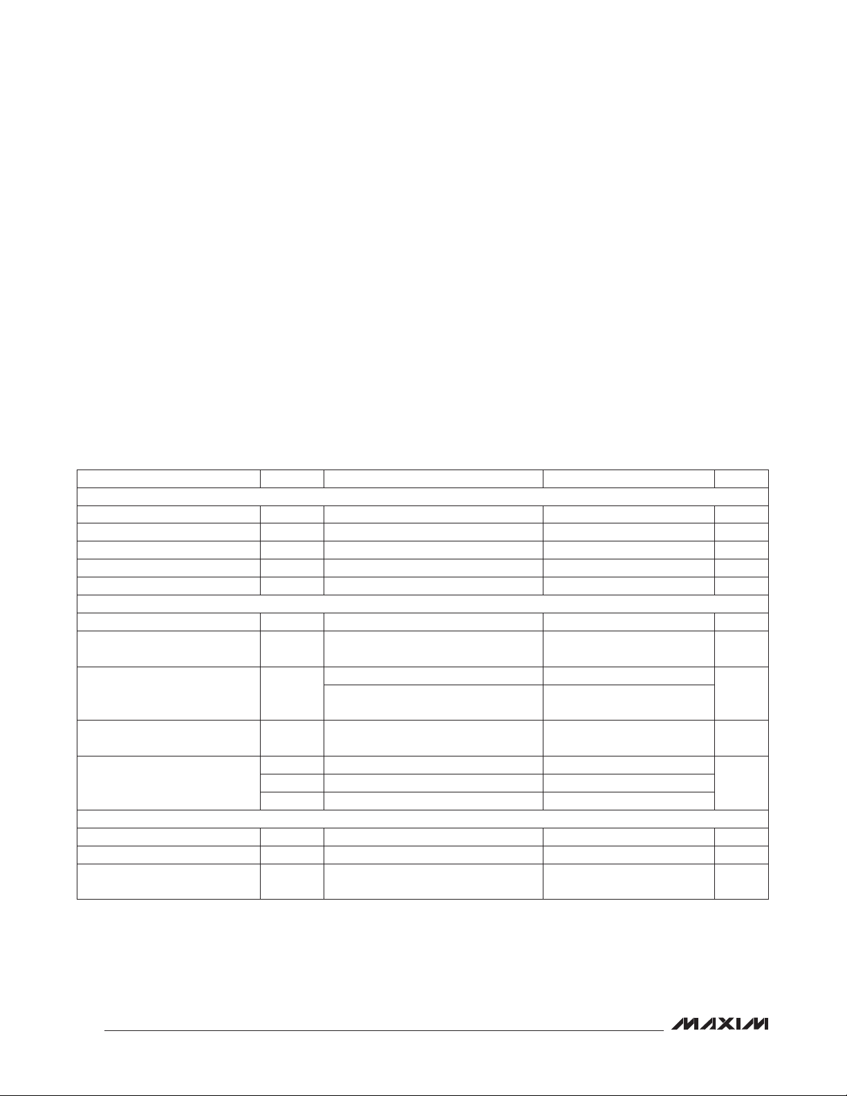
ELECTRICAL CHARACTERISTICS
(V
= 1.8V, V
AVDD
registers at default settings (Table 1), TA = -40NC to +85NC, typical values are at TA = +25NC, unless otherwise noted.) (Note 1)
PARAMETER SYMBOL CONDITIONS MIN TYP MAX UNITS
DC ACCURACY
Resolution 12 Bits
Integral Nonlinearity INL fIN = 5.3MHz
Differential Nonlinearity DNL fIN = 5.3MHz, no missing codes
Offset Error OE Internal reference
Gain Error GE External reference = 1.25V
ANALOG INPUTS (IN_+, IN_-) (Figure 2)
Input Differential Range V
Common-Mode Input Voltage
Range
Input Resistance R
Input Current I
Input Capacitance
CONVERSION RATE
Maximum Clock Frequency f
Minimum Clock Frequency f
Data Latency Figure 5 8.5
= 1.8V, internal reference, AIN = -0.5dBFS, differential clock, V
OVDD
DIFF
V
C
C
SAMPLE
CLK
CLK
IN_+ - IN_- 1.5 V
Q50mV tolerance
CM
Fixed resistance to GND > 100
Differential input resistance, common
IN
mode connected to inputs
Switched capacitance input current,
IN
each input, V
Fixed capacitance to GND, each input 1
INS
Fixed differential capacitance 0.2
IND
Switched capacitance, each input 1.5
CM
Continuous Power Dissipation (TA = +70NC)
144-Lead CTBGA (derate 37mW/NC above +70NC)
Multilayer Board ...................................................... 2963mW
Operating Temperature Range ......................... -40NC to +85NC
Junction Temperature ....................................................+150NC
Storage Temperature Range .......................... -65NC to +150NC
Lead Temperature (soldering, 10s) ................................+300NC
Soldering Temperature (reflow) ......................................+260NC
= 1.050V
CLKD
= 1.5V
, f
P-P
50 MHz
= 50MHz, programmable
CLK
Q0.5 Q1.7
Q0.3 Q1.0
Q0.07 Q0.7
Q0.2 Q3.0
1050 mV
4
36
25 MHz
LSB
LSB
%FS
%FS
P-P
kI
FA
pFC
Clock
Cycles
2
Page 3
Ultra-Low-Power, Octal, 12-Bit, 50Msps,
1.8V ADC with Serial LVDS Outputs
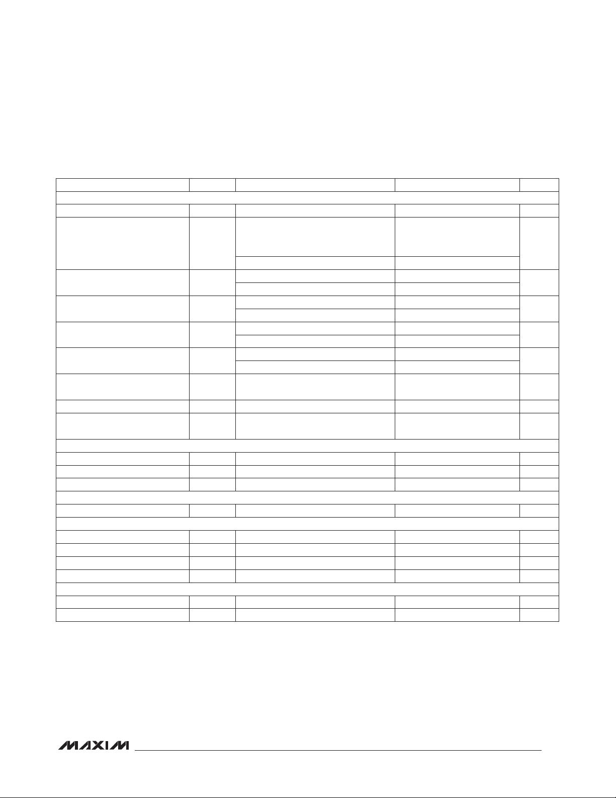
ELECTRICAL CHARACTERISTICS (continued)
(V
= 1.8V, V
AVDD
registers at default settings (Table 1), TA = -40NC to +85NC, typical values are at TA = +25NC, unless otherwise noted.) (Note 1)
PARAMETER SYMBOL CONDITIONS MIN TYP MAX UNITS
DYNAMIC PERFORMANCE
Small-Signal Noise Floor SSNF Analog input < -35dBFS, fIN = 5.3MHz -69.5 dBFS
Near-Carrier Signal-to-Noise
Ratio
Signal-to-Noise Ratio SNR
Signal-to-Noise and Distortion
Ratio
Spurious-Free Dynamic Range SFDR
Total Harmonic Distortion THD
Intermodulation Distortion IMD
Full-Power Bandwidth FPBW
Overdrive Recovery Time
INTERCHANNEL CHARACTERISTICS
Crosstalk fIN = 5.3MHz at -0.5dBFS -90 dB
Gain Matching fIN = 5.3MHz
Phase Matching fIN = 5.3MHz
ANALOG OUTPUT (CMOUT)
CMOUT Output Voltage V
INTERNAL REFERENCE
REFIO Output Voltage V
REFIO Temperature Coefficient TC
REFH Voltage V
REFL Voltage V
EXTERNAL REFERENCE
REFIO Input Voltage Range V
REFIO Input Resistance R
= 1.8V, internal reference, AIN = -0.5dBFS, differential clock, V
OVDD
1kHz offset from 5.3MHz full-scale tone,
C
NCSNR
SINAD
CMOUT
REFIO
REF
REFH
REFL
REFIN
REFIN
= C
REFIO
(Figure 3)
8-channel coherent sum 147
fIN = 5.3MHz at -0.5dBFS 67.0 68.5
fIN = 19.3MHz at -0.5dBFS 68.5
fIN = 5.3MHz at -0.5dBFS 66.6 68.2
fIN = 19.3MHz at -0.5dBFS 68.2
fIN = 5.3MHz at -0.5dBFS 70.0 84
fIN = 19.3MHz at -0.5dBFS 84
fIN = 5.3MHz at -0.5dBFS -81 -72
fIN = 19.3MHz at -0.5dBFS -81
f
= 5.15MHz at -6.5dBFS,
IN1
f
= 5.45MHz at -6.5dBFS
IN2
R
SOURCE
6dB beyond full scale (recover accuracy
to < 1% of full scale)
Default programming state 1.05 1.10 1.15 V
Bypass only, no DC load 1.22 1.25 1.28 V
Bypass only, no DC load 1.61 V
Bypass only, no DC load 0.86 V
+5%/-15% tolerance 1.25 V
REFH/REFL
= 50I differential
= 0.1FF
CLKD
= 1.5V
, f
P-P
= 50MHz, programmable
CLK
140
-83 dB
> 500 MHz
< 1
Q0.1
Q0.25
< Q60 ppm/NC
10 Q 20% kI
dBc/Hz
dB
dB
dBc
dBc
Clock
Cycles
dB
Degrees
MAX19527
3
Page 4
Ultra-Low-Power, Octal, 12-Bit, 50Msps,
1.8V ADC with Serial LVDS Outputs
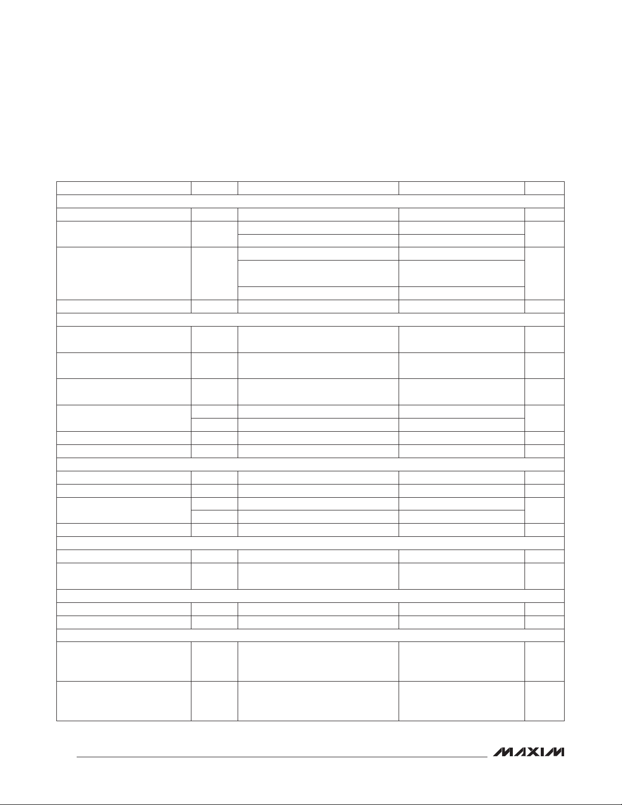
ELECTRICAL CHARACTERISTICS (continued)
(V
= 1.8V, V
AVDD
registers at default settings (Table 1), TA = -40NC to +85NC, typical values are at TA = +25NC, unless otherwise noted.) (Note 1)
PARAMETER SYMBOL CONDITIONS MIN TYP MAX UNITS
CLOCK INPUTS (CLKIN+, CLKIN-)—DIFFERENTIAL MODE (Figure 4)
Differential Clock Input Voltage V
Common-Mode Voltage V
MAX19527
Input Resistance R
Input Capacitance C
CLOCK INPUTS (CLKIN+, CLKIN-)—SINGLE-ENDED MODE (CLKIN- < 0.1V) (Figure 4)
Single-Ended Mode Selection
Threshold (CLKIN-)
Single-Ended Clock Input High
Threshold (CLKIN+)
Single-Ended Clock Input Low
Threshold (CLKIN+)
Input Leakage (CLKIN+)
Input Leakage (CLKIN-) I
Input Capacitance (CLKIN+) 3 pF
DIGITAL INPUTS (SHDN, SCLK, SDIN, CS)
Input High Threshold V
Input Low Threshold V
Input Leakage
Input Capacitance C
DIGITAL OUTPUTS (SDIO)
Output Voltage Low V
Output Voltage High V
LVDS DIGITAL OUTPUTS (OUT_+/OUT_-, CLKOUT+/CLKOUT-, FRAME+/FRAME-)
Differential Output Voltage |VOD|
Output Offset Voltage V
POWER-MANAGEMENT CHARACTERISTICS (Figure 3)
Wake-Up Time from Sleep Mode t
Wake-Up Time from Nap Mode t
= 1.8V, internal reference, AIN = -0.5dBFS, differential clock, V
OVDD
CLKD
CLKCM
V
V
V
I
I
SWAKE
NWAKE
Self-biased 1.2
DC-coupled clock signal 1.0 to 1.4
Differential, default setting 10
Differential, programmable internal
CLK
termination selected
Common mode to GND 9
Capacitance to GND, each input 3 pF
CLK
IL
IH
IL
VIH = 1.8V +5
IH
I
VIH = 0V -5
IL
VIH = 0V -150 -50
IL
IH
IL
VIH = 1.8V +5
IH
I
VIL = 0V -5
IL
DIN
I
OL
OH
OS
= 200FA
SINK
I
SOURCE
External R
External R
Internal reference, C
C
with respect to steady-state gain
Internal reference, C
C
with respect to steady-state gain
= 200FA
REFH/REFL
REFH/REFL
= 100I
LOAD
= 100I
LOAD
REFIO
= 0.1FF; Q1% gain error,
REFIO
= 0.1FF; Q1% gain error,
= 0.1FF,
= 0.1FF,
= 1.5V
CLKD
OVDD -
250 450 mV
1.125 1.375 V
, f
P-P
1.5 V
1.5 V
0.2
= 50MHz, programmable
CLK
0.4 to 2.0 V
0.1
3 pF
10 ms
2
0.1 V
0.3 V
0.3 V
0.2 V
P-P
V
kI
FA
FA
FA
V
Fs
4
Page 5
Ultra-Low-Power, Octal, 12-Bit, 50Msps,
1.8V ADC with Serial LVDS Outputs
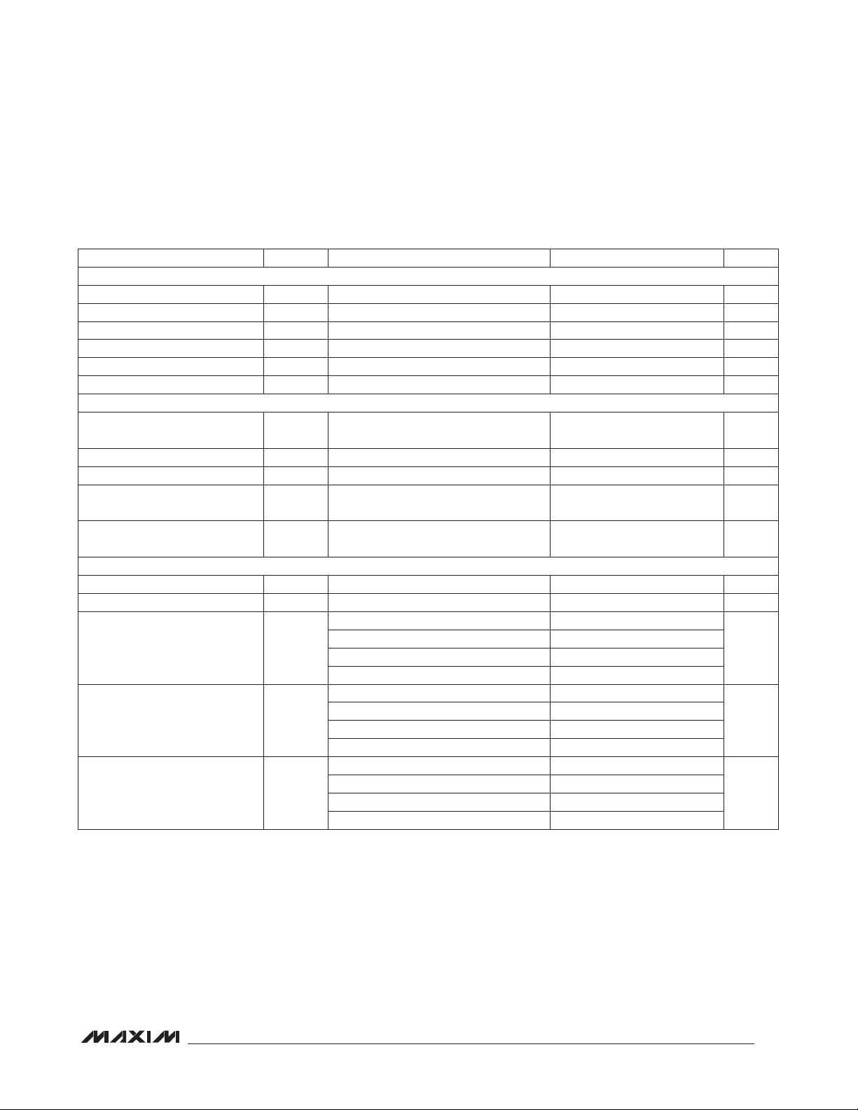
ELECTRICAL CHARACTERISTICS (continued)
(V
= 1.8V, V
AVDD
registers at default settings (Table 1), TA = -40NC to +85NC, typical values are at TA = +25NC, unless otherwise noted.) (Note 1)
PARAMETER SYMBOL CONDITIONS MIN TYP MAX UNITS
SERIAL PERIPHERAL INTERFACE (SPI) TIMING (Figure 9, Note 2)
SCLK Period t
SCLK to CS Setup Time
SCLK to CS Hold Time
SDIO to SCLK Setup Time t
SDIO to SCLK Hold Time t
SCLK to SDIO Output Data Delay t
TIMING CHARACTERISTICS (Figures 6 and 7, Note 2)
Data Valid to CLKOUT Rise/Fall t
CLKOUT Output-Width High t
CLKOUT Output-Width Low t
FRAME Rise to CLKOUT Rise t
Sample CLK Rise to Frame Rise t
POWER REQUIREMENTS
Analog Supply Voltage V
Digital Output Supply Voltage V
Analog Supply Current I
Digital Output Supply Current I
Total Power Dissipation P
Note 1: Specifications are 100% production tested at TA R +25NC. Specifications for TA < +25NC are guaranteed by design and
characterization.
Note 2: Specifications guaranteed by design and characterization.
= 1.8V, internal reference, AIN = -0.5dBFS, differential clock, V
OVDD
SCLK
t
CSS
t
CSH
SDS
SDH
SDD
AVDD
OVDD
AVDD
OVDD
Serial-data write 10 ns
Serial-data write 0 ns
Serial-data read 10 ns
OD
CH
CL
DF
SF
8 channels active 158 180
Incremental channel power-down -18
Nap mode 13 15
Sleep mode 0.35 0.5
8 channels active, external R
Incremental channel power-down -7.4
Nap mode 28
Sleep mode < 0.1
8 channels active 440
Incremental channel power-down -46
TD
Nap mode 74
Sleep mode 0.8
LOAD
CLKD
= 100I
= 1.5V
t
SAMPLE
24 - 0.10
t
SAMPLE
24 - 0.10
t
SAMPLE
2 + 1.6
, f
P-P
50 ns
10 ns
10 ns
/
/
/
1.7 1.8 1.9 V
1.7 1.8 1.9 V
= 50MHz, programmable
CLK
t
24 + 0.05
t
SAMPLE
t
SAMPLE
t
SAMPLE
24 + 0.05
t
SAMPLE
/
SAMPLE
2 + 2.3
t
24 + 0.20
/12 ns
/12 ns
/
t
24 + 0.20
/
t
87
SAMPLE
SAMPLE
SAMPLE
2 + 3.3
/
ns
/
ns
/
ns
mA
mA
mW
MAX19527
5
Page 6
Ultra-Low-Power, Octal, 12-Bit, 50Msps,
1.8V ADC with Serial LVDS Outputs
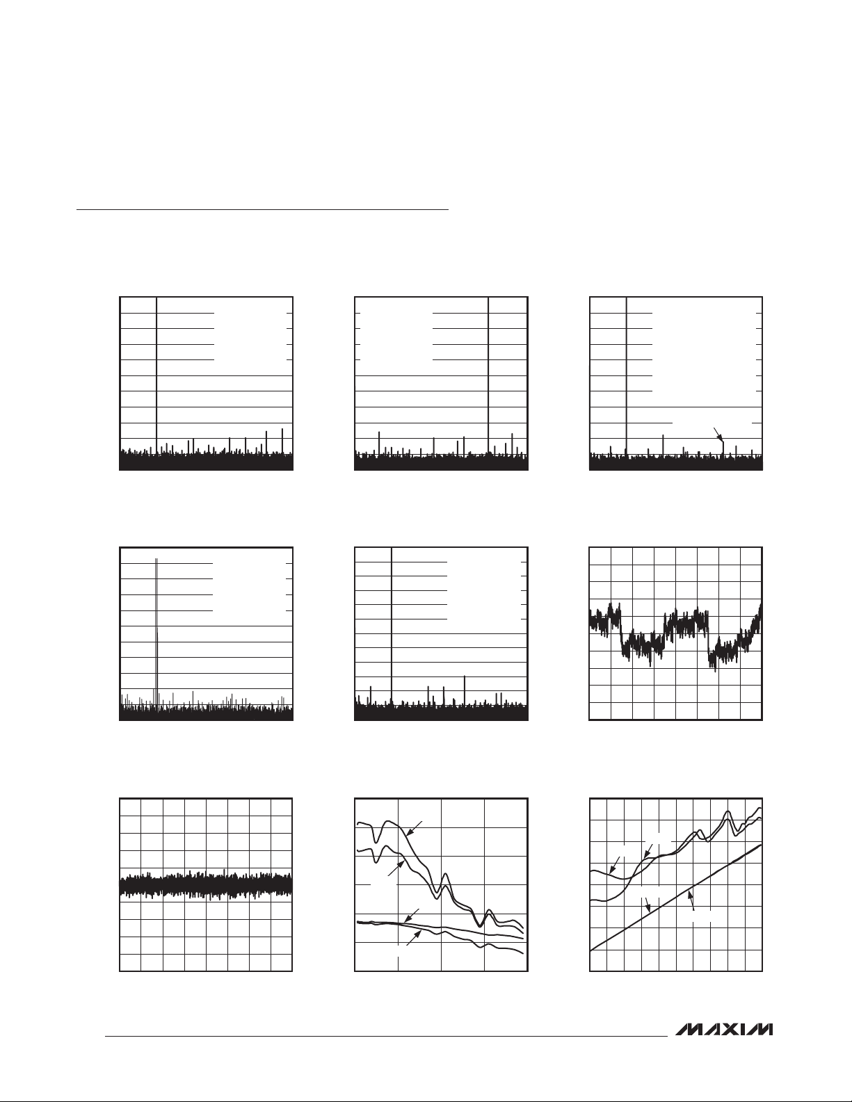
Typical Operating Characteristics
(V
= 1.8V, V
AVDD
registers at default settings (Table 1), TA = -40NC to +85NC, typical values are at TA = +25NC, unless otherwise noted. Specifications
are 100% production tested at TA R +25NC. Specifications for TA < +25NC are guaranteed by design and characterization.)
= 1.8V, internal reference, AIN = -0.5dBFS, differential clock, V
OVDD
CLKD
= 1.5V
P-P
, f
= 50MHz, programmable
CLK
0
-10
-20
MAX19527
-30
-40
-50
-60
-70
AMPLITUDE (dBFS)
-80
-90
-100
-110
0 25
FREQUENCY (MHz)
TWO-TONE INTERMODULATION
DISTORTION
0
-10
-20
-30
-40
-50
-60
-70
AMPLITUDE (dBFS)
-80
-90
-100
-110
0 25
FREQUENCY (MHz)
5.3MHz INPUT FFT PLOT
fIN = 5.301324MHz
AIN = -0.49dBFS
SNR = 68.58dB
SINAD = 68.35dB
THD = -81.19dBc
SFDR = 85.17dB
2015105
f
= 5.154828MHz
IN1
f
= 5.423404MHz
IN2
A
= -6.95dBFS
IN1
A
= -7.02dBFS
IN2
IM3 = -83dBc
2015105
MAX19527 toc01
AMPLITUDE (dBFS)
-100
-110
MAX19527 toc04
AMPLITUDE (dBFS)
-100
-110
-120
19.3MHz INPUT FFT PLOT
0
fIN = 19.303900MHz
-10
AIN = -0.51dBFS
-20
SNR = 68.49dB
SINAD = 68.24dB
-30
THD = -80.90dBc
-40
SFDR = 85.73dB
-50
-60
-70
-80
-90
0 25
FREQUENCY (MHz)
5.3MHz INPUT FFT PLOT
8-CHANNEL COHERENT SUM
0
-10
-20
-30
-40
-50
-60
-70
-80
-90
0 25
FREQUENCY (MHz)
fIN = 5.301324MHz
A
= -0.50dBFS
IN
SNR = 77.20dB
SINAD = 76.84dB
THD = -87.80dBc
SFDR = 89.31dB
0
-10
-20
MAX19527 toc02
-30
-40
-50
-60
-70
AMPLITUDE (dBFS)
-80
-90
-100
-110
2015105
0 25
MEASURED ON CHANNEL 1,
WITH INTERFERING SIGNAL
FREQUENCY (MHz)
ON CHANNEL 2
f
= 5.301324MHz
IN(IN1)
f
= 19.303900MHz
IN(IN2)
= -0.5dBFS
A
IN(IN1)
A
= -0.5dBFS
IN(IN2)
CROSSTALK = -92dB
f
= 19.3039MHz
IN(IN2)
MAX19527 toc03
2015105
INTEGRAL NONLINEARITY
vs. DIGITAL OUTPUT CODE
1.0
0.8
CROSSTALK FFT PLOT
MAX19527 toc05
0.6
0.4
0.2
0
INL (LSB)
-0.2
-0.4
-0.6
-0.8
2015105
-1.0
0 4096
DIGITAL OUTPUT CODE
MAX19527 toc06
358430722048 25601024 1536512
DIFFERENTIAL NONLINEARITY
vs. DIGITAL OUTPUT CODE
1.0
0.8
0.6
0.4
0.2
0
DNL (LSB)
-0.2
-0.4
-0.6
-0.8
-1.0
0 4096
DIGITAL OUTPUT CODE
6
DYNAMIC PERFORMANCE
vs. INPUT FREQUENCY
90
85
MAX19527 toc07
80
75
70
DYNAMIC PERFORMANCE (dB)
65
358430722048 25601024 1536512
60
0 200
SFDR
-THD
SNR
SINAD
15010050
INPUT FREQUENCY (MHz)
90
80
MAX195027 toc08
70
60
50
40
30
DYNAMIC PERFORMANCE (dB)
20
10
DYNAMIC PERFORMANCE
vs. ANALOG INPUT POWER
SFDR
-THD
SNR
SINAD
-50 0
ANALOG INPUT POWER (dBFS)
-5-10-45 -40 -35 -25 -20-30 -15
MAX19527 toc09
Page 7
Ultra-Low-Power, Octal, 12-Bit, 50Msps,
1.8V ADC with Serial LVDS Outputs
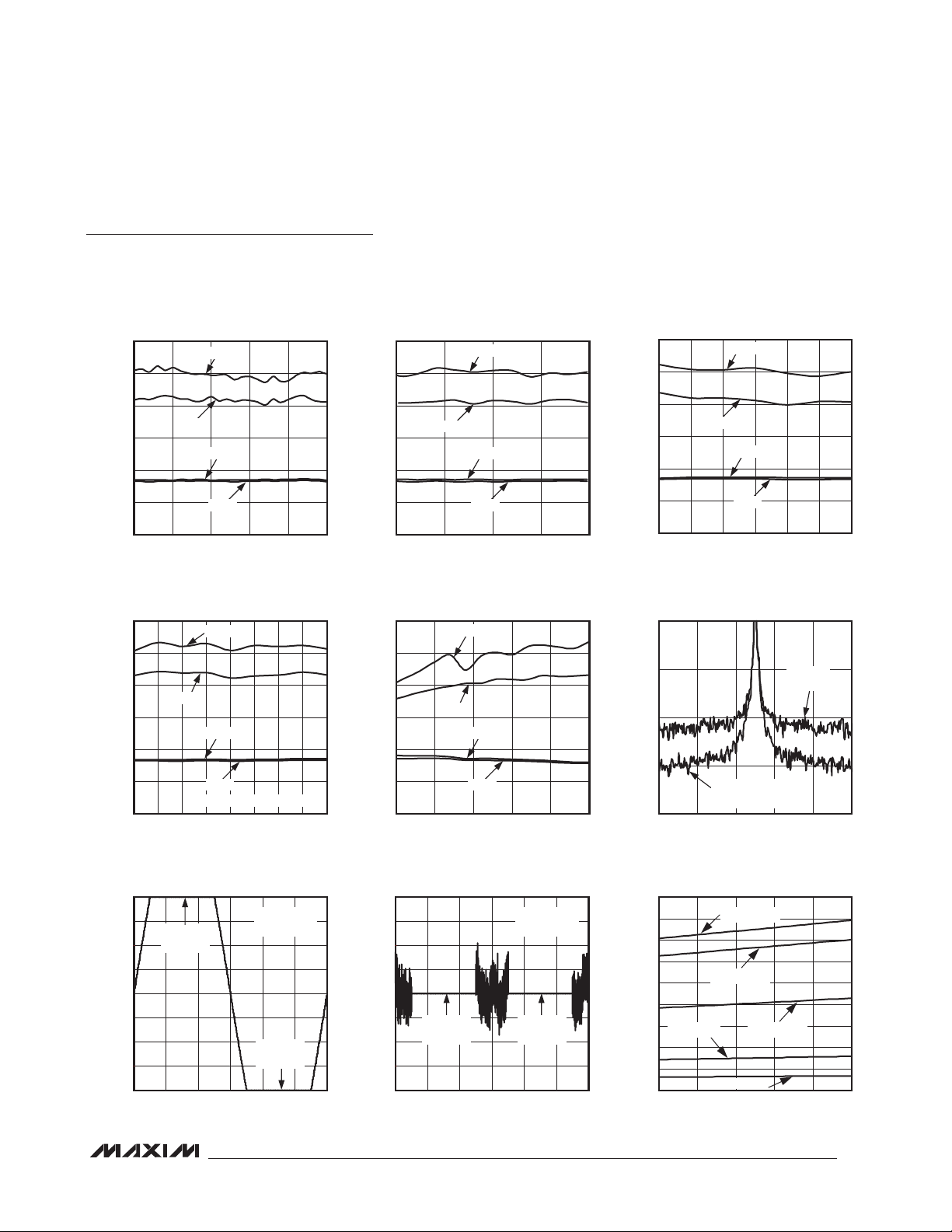
Typical Operating Characteristics (continued)
(V
= 1.8V, V
AVDD
registers at default settings (Table 1), TA = -40NC to +85NC, typical values are at TA = +25NC, unless otherwise noted. Specifications
are 100% production tested at TA R +25NC. Specifications for TA < +25NC are guaranteed by design and characterization.)
DYNAMIC PERFORMANCE
90
85
80
75
70
DYNAMIC PERFORMANCE (dB)
65
= 1.8V, internal reference, AIN = -0.5dBFS, differential clock, V
OVDD
DYNAMIC PERFORMANCE
vs. SAMPLING RATE
SFDR
MAX19527 toc10
-THD
SNR
SINAD
vs. INPUT COMMON-MODE VOLTAGE
90
85
80
75
70
DYNAMIC PERFORMANCE (dB)
65
SFDR
-THD
SNR
SINAD
= 1.5V
CLKD
MAX19527 toc11
P-P
90
85
80
75
70
DYNAMIC PERFORMANCE (dB)
65
, f
= 50MHz, programmable
CLK
DYNAMIC PERFORMANCE
vs. ANALOG SUPPLY VOLTAGE
SFDR
-THD
SNR
SINAD
MAX19527
MAX19527 toc12
60
25 50
SAMPLING RATE (MHz)
DYNAMIC PERFORMANCE
vs. CLOCK DUTY CYCLE
90
85
80
75
70
DYNAMIC PERFORMANCE (dB)
65
60
SFDR
-THD
SNR
SINAD
SINGLE-ENDED CLOCK MODE
CLOCK DUTY CYCLE (%)
+6dB OVERDRIVE
OUTPUT CODE vs. SIGNAL PHASE
4096
3584
3072
2560
2048
1536
1024
+6dB OVERDRIVE OUTPUT CODE
512
CLIPPED AT
4095
CLIPPED AT
0
0 360
SIGNAL PHASE (DEGREES)
240 30018060 120
45403530
60555045403530 70
65
fIN = 5.3MHz
AIN = +6dBFS
0
60
INPUT COMMON-MODE VOLTAGE (V)
90
85
MAX19527 toc13
80
75
70
DYNAMIC PERFORMANCE (dB)
65
60
-40 85
1.00
0.75
MAX19527 toc16
0.50
0.25
0
-0.25
-0.50
+6dB OVERDRIVE ERROR (LSB)
-0.75
-1.00
0 360
1.051.000.95 1.15
1.10
DYNAMIC PERFORMANCE
vs. TEMPERATURE
SFDR
-THD
SNR
SINAD
TEMPERATURE (°C)
+6dB OVERDRIVE
ERROR vs. SIGNAL PHASE
fIN = 5.3MHz
AIN = +6dBFS
CLIPPED AT
4095
SIGNAL PHASE (DEGREES)
CLIPPED AT
240 30018060 120
60
V
AVDD
(V)
1.851.801.751.701.65 1.95
1.90
NEAR-CARRIER NOISE SPECTRUM
vs. FREQUENCY OFFSET
-120
MAX19527 toc14
-130
-140
-150
NEAR-CARRIER NOISE SPECTRUM (dBC/Hz)
603510-15
-160
-5 5
8-CHANNEL
COHERENT SUM
FREQUENCY OFFSET (kHz)
SINGLE
CHANNEL
31-1-3
MAX19527 toc15
ANALOG SUPPLY CURRENT
vs. SAMPLING RATE (AVDD)
180
160
MAX19527 toc17
140
120
100
80
60
0
ANALOG SUPPLY CURRENT (mA)
1 CHANNEL
40
20
0
25 50
8 CHANNELS
MAX19527 toc18
7 CHANNELS
4 CHANNELS
NAP MODE
45403530
SAMPLING RATE (MHz)
7
Page 8
Ultra-Low-Power, Octal, 12-Bit, 50Msps,
CMOUT VOLTAGE (V)
1.8V ADC with Serial LVDS Outputs
Typical Operating Characteristics (continued)
(V
= 1.8V, V
AVDD
registers at default settings (Table 1), TA = -40NC to +85NC, typical values are at TA = +25NC, unless otherwise noted. Specifications
are 100% production tested at TA R +25NC. Specifications for TA < +25NC are guaranteed by design and characterization.)
ANALOG SUPPLY CURRENT
vs. TEMPERATURE (AVDD)
180
175
170
MAX19527
165
160
155
150
ANALOG SUPPLY CURRENT (mA)
145
140
-40 85
DIGITAL SUPPLY CURRENT
vs. TEMPERATURE (OVDD)
95
= 1.8V, internal reference, AIN = -0.5dBFS, differential clock, V
OVDD
ANALOG SUPPLY CURRENT
vs. SUPPLY VOLTAGE (AVDD)
170
165
MAX19527 toc19
160
155
150
ANALOG SUPPLY CURRENT (mA)
145
140
6035-15 10
TEMPERATURE (°C)
1.65 1.95
SUPPLY VOLTAGE (V)
DIGITAL SUPPLY CURRENT
vs. SUPPLY VOLTAGE (OVDD)
100
CLKD
= 1.5V
P-P
, f
= 50MHz, programmable
CLK
DIGITAL SUPPLY CURRENT
vs. SAMPLING RATE (OVDD)
100
90
MAX19527 toc20
80
70
60
50
40
30
DIGITAL SUPPLY CURRENT (mA)
20
10
0
1.901.851.801.751.70
25 50
8 CHANNELS
7 CHANNELS
4 CHANNELS
1 CHANNEL
NAP MODE
SAMPLING RATE (MHz)
REFERENCE VOLTAGE
vs. TEMPERATURE
1.260
MAX19527 toc21
45403530
90
85
80
DIGITAL SUPPLY CURRENT (mA)
75
-40 85
TEMPERATURE (°C)
CMOUT VOLTAGE
vs. TEMPERATURE
1.18
1.16
1.14
1.12
1.10
1.08
1.06
CMOUT VOLTAGE (V)
1.04
1.02
1.00
111
110
101
100
011
010
001
000
-40 80
TEMPERATURE (°C)
8
603510-15
CMI_ADJ[2:0]
6040200-20
95
MAX19527 toc22
90
85
80
DIGITAL SUPPLY CURRENT (mA)
75
70
1.65 1.95
1.12
MAX19527 toc25
1.11
1.10
1.09
1.08
1.07
0 1000
1.901.851.801.751.70
SUPPLY VOLTAGE (V)
CMOUT VOLTAGE
vs. CMOUT LOAD CURRENT
800600400200
CMOUT LOAD CURRENT (µA)
MAX19527 toc23
1.255
1.250
1.245
REFERENCE VOLTAGE (V)
1.240
1.230
-40 85
50
45
MAX19527 toc26
40
35
30
ANALOG INPUT CURRENT (µA)
25
20
0.95 1.15
MAX19527 toc24
603510-15
TEMPERATURE (°C)
ANALOG INPUT CURRENT
vs. INPUT COMMON-MODE
VOLTAGE (AVDD)
MAX19527 toc27
1.101.051.00
INPUT COMMON-MODE VOLTAGE (V)
Page 9
Ultra-Low-Power, Octal, 12-Bit, 50Msps,
1.8V ADC with Serial LVDS Outputs
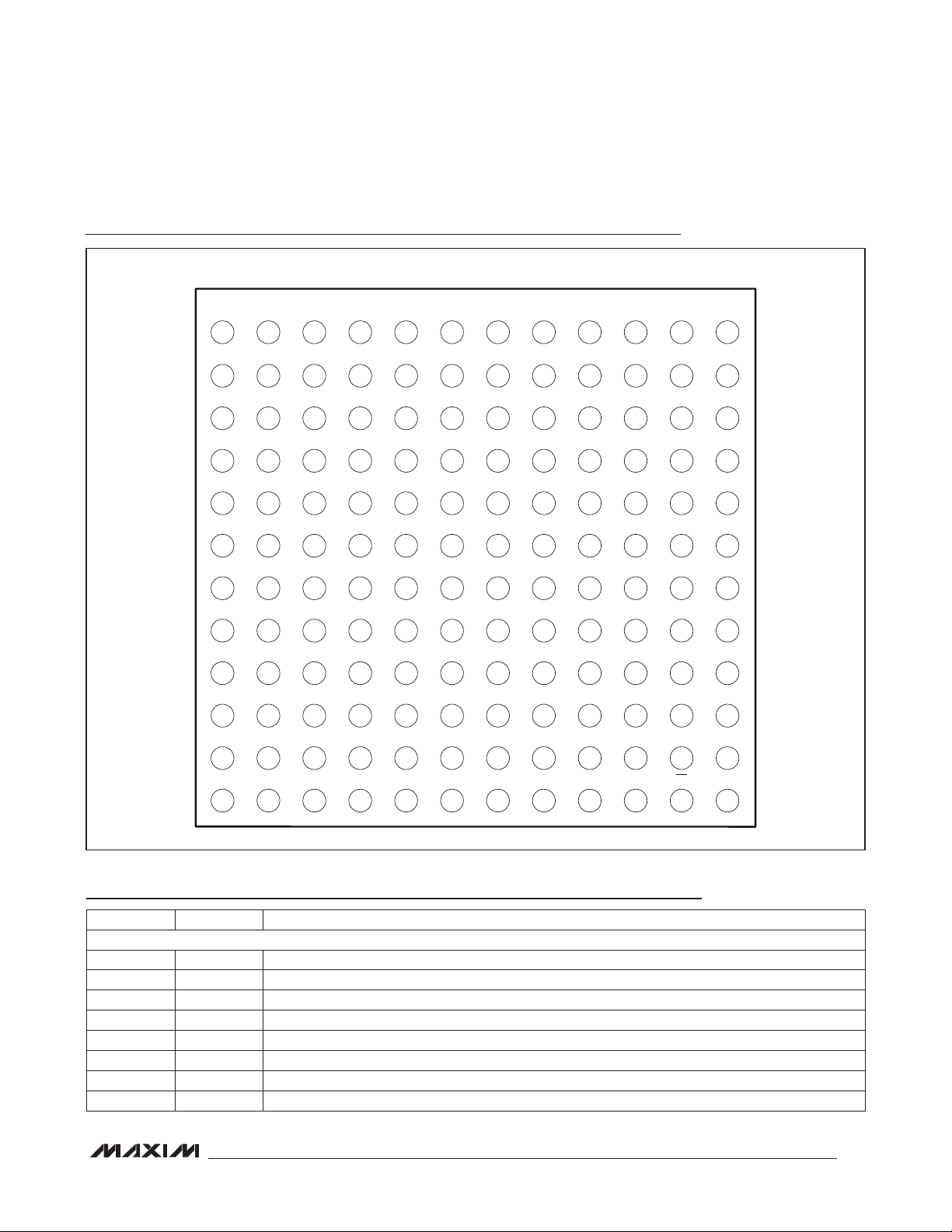
Pin Configuration
TOP VIEW
REFLN.C. N.C.N.C. OGNDN.C.N.C. N.C. REFH REFIO OVDDAVDD
A1 A2 A3 A4 A5 A6 A7 A8 A9 A10 A11 A12
SHDNN.C. N.C. N.C. N.C. N.C. N.C. OUT1+AVDD I.C. OUT1-N.C.
B1 B2 B3 B4 B5 B6 B7 B8 B9 B10 B11 B12
IN1- GNDGND GNDIN1+ GND GND GND GND OGND OUT2+ OUT2-
C1 C2 C3 C4 C5 C6 C7 C8 C9 C10 C11 C12
GND OGND OUT3+ OUT3-IN2- GND GND GND GND GND GNDIN2+
D1 D2 D3 D4 D5 D6 D7 D8 D9 D10 D11 D12
GND OGND OUT4+ OUT4-IN3- GND GND GND GND GND GNDIN3+
E1 E2 E3 E4 E5 E6 E7 E8 E9 E10 E11 E12
GND OVDD CLKOUT+ CLKOUT-IN4- CMOUT GND GND GND AVDD GNDIN4+
F1 F2 F3 F4 F5 F6 F7 F8 F9 F10 F11 F12
GND OVDD FRAME+ FRAME-IN5- CMOUT GND GND GND AVDD GNDIN5+
G1 G2 G3 G4 G5 G6 G7 G8 G9 G10 G11 G12
GND OGND OUT5+ OUT5-IN6- GND GND GND GND GND GNDIN6+
H1 H2 H3 H4 H5 H6 H7 H8 H9 H10 H11 H12
GND OGND OUT6+ OUT6-IN7- GND GND GND GND GND GNDIN7+
J1 J2 J3 J4 J5 J6 J7 J8 J9 J10 J11 J12
GND OGND OUT7+ OUT7-IN8- GND GND GND GND GND GNDIN8+
K1 K2 K3 K4 K5 K6 K7 K8 K9 K10 K11 K12
SDION.C. N.C.N.C. OUT8+N.C. N.C.N.C. GND OUT8-AVDD CLKIN+
L1 L2 L3 L4 L5 L6 L7 L8 L9 L10 L11 L12
SCLKN.C. N.C.N.C. CSN.C. N.C.N.C. GND OVDDAVDD CLKIN-
M1 M2 M3 M4 M5 M6 M7 M8 M9 M10 M11 M12
MAX19527
Pin Description
PIN NAME FUNCTION
ANALOG INPUTS
C1 IN1- Channel 1 Negative (Inverting) Analog Input
C2 IN1+ Channel 1 Positive (Noninverting) Analog Input
D1 IN2- Channel 2 Negative (Inverting) Analog Input
D2 IN2+ Channel 2 Positive (Noninverting) Analog Input
E1 IN3- Channel 3 Negative (Inverting) Analog Input
E2 IN3+ Channel 3 Positive (Noninverting) Analog Input
F1 IN4- Channel 4 Negative (Inverting) Analog Input
F2 IN4+ Channel 4 Positive (Noninverting) Analog Input
9
Page 10

Ultra-Low-Power, Octal, 12-Bit, 50Msps,
1.8V ADC with Serial LVDS Outputs
Pin Description (continued)
PIN NAME FUNCTION
G1 IN5- Channel 5 Negative (Inverting) Analog Input
G2 IN5+ Channel 5 Positive (Noninverting) Analog Input
H1 IN6- Channel 6 Negative (Inverting) Analog Input
H2 IN6+ Channel 6 Positive (Noninverting) Analog Input
J1 IN7- Channel 7 Negative (Inverting) Analog Input
MAX19527
J2 IN7+ Channel 7 Positive (Noninverting) Analog Input
K1 IN8- Channel 8 Negative (Inverting) Analog Input
K2 IN8+ Channel 8 Positive (Noninverting) Analog Input
L8 CLKIN+ Clock Positive (Noninverting) Input
M8 CLKIN-
LVDS OUTPUTS
B11 OUT1+ Channel 1 Positive (Noninverting) LVDS Digital Output
B12 OUT1- Channel 1 Negative (Inverting) LVDS Digital Output
C11 OUT2+ Channel 2 Positive (Noninverting) LVDS Digital Output
C12 OUT2- Channel 2 Negative (Inverting) LVDS Digital Output
D11 OUT3+ Channel 3 Positive (Noninverting) LVDS Digital Output
D12 OUT3- Channel 3 Negative (Inverting) LVDS Digital Output
E11 OUT4+ Channel 4 Positive (Noninverting) LVDS Digital Output
E12 OUT4- Channel 4 Negative (Inverting) LVDS Digital Output
F11 CLKOUT+ Positive (Noninverting) Serial LVDS Clock Output
F12 CLKOUT- Negative (Inverting) Serial LVDS Clock Output
G11 FRAME+
G12 FRAME-
H11 OUT5+ Channel 5 Positive (Noninverting) LVDS Digital Output
H12 OUT5- Channel 5 Negative (Inverting) LVDS Digital Output
J11 OUT6+ Channel 6 Positive (Noninverting) LVDS Digital Output
J12 OUT6- Channel 6 Negative (Inverting) LVDS Digital Output
K11 OUT7+ Channel 7 Positive (Noninverting) LVDS Digital Output
K12 OUT7- Channel 7 Negative (Inverting) LVDS Digital Output
L11 OUT8+ Channel 8 Positive (Noninverting) LVDS Digital Output
L12 OUT8- Channel 8 Negative (Inverting) LVDS Digital Output
3-WIRE SERIAL PERIPHERAL INTERFACE (SPI)
L10 SDIO SPI Data Input/Output
M10 SCLK SPI Clock
M11
CS
Clock Negative (Inverting) Input. If CLKIN- is connected to ground, CLKIN+ is a single-ended,
logic-level clock input. Otherwise, CLKIN+ and CLKIN- are self-biased differential clock inputs.
Positive (Noninverting) Frame-Alignment LVDS Output. A rising edge on the differential FRAME
output aligns to a valid output data frame.
Negative (Inverting) Frame-Alignment LVDS Output. A rising edge on the differential FRAME output
aligns to a valid output data frame.
SPI Chip Select
10
Page 11

Ultra-Low-Power, Octal, 12-Bit, 50Msps,
1.8V ADC with Serial LVDS Outputs
Pin Description (continued)
PIN NAME FUNCTION
REFERENCE
A8 REFH
A9 REFIO
A10 REFL
SUPPLY AND BIAS
A7, B8, F7,
G7, L7, M7
A11, C10,
D10, E10,
H10, J10,
K10
A12, F10,
G10, M12
B10 SHDN
C3–C9, D3–
D9, E3–E9,
F4, F5, F6,
F8, F9, G4,
G5, G6, G8,
G9, H3–H9,
J3–J9, K3–
K9, L9, M9
F3, G3 CMOUT
OTHER
A1–A6, B1–
B7, L1–L6,
M1–M6
B9 I.C. Internal Connection. Leave I.C. unconnected.
AVDD
OGND
OVDD
GND
N.C. No Connection. Not internally connected.
High Reference Bypass. Bypass REFH with a 0.1FF capacitor to REFL. See the Reference
Configurations section for details.
Reference Input/Output. To use internal reference, bypass to GND with a capacitor value of 0.1 FF.
See the Reference Configurations section for an external reference.
Low Reference Bypass. Bypass REFL with a 0.1FF capacitor to REFH. See the Reference
Configurations section for details.
Analog Supply Voltage. Apply 1.8V to all AVDD inputs. Bypass each input to GND with a 0.1FF
capacitor.
Digital Ground. Connect all GND (analog ground) and OGND (digital ground) pins to the board
ground plane.
Digital Supply Voltage. Digital and output driver supply input. Apply 1.8V to all OVDD inputs.
Bypass each input to GND with a 0.1FF capacitor.
Active-High Power-Down. Programmable power-management state selection. See the Power
Management section for details.
Analog Ground. Connect all GND (analog ground) and OGND (digital ground) pins to the board
ground plane.
Common-Mode Output. Input common-mode reference output. Bypass CMOUT with a 1FF
capacitor to GND.
MAX19527
11
Page 12

Ultra-Low-Power, Octal, 12-Bit, 50Msps,
1.8V ADC with Serial LVDS Outputs
Simplified Block Diagram
REFIO
REFH REFL CS SCLK SDIO SHDN
MAX19527
CMOUT
IN1+
IN1-
IN2+
IN2-
IN8+
IN8-
CLKIN+
CLKIN-
REFERENCE AND
BIAS GENERATION
12-BIT
ADC
12-BIT
ADC
12-BIT
ADC
CLOCK
CIRCUITRY
SPI, REGISTERS,
AND CONTROL
DIGITAL SERIALIZER
DIGITAL SERIALIZER
DIGITAL
PLL
AVDD OVDD GND
SERIALIZER
6x
MAX19527
1x
LVDS
LVDS
LVDS
LVDS
LVDS
OUT1+
OUT1-
OUT2+
OUT2-
OUT8+
OUT8-
CLKOUT+
CLKOUT-
FRAME+
FRAME-
12
Page 13

Ultra-Low-Power, Octal, 12-Bit, 50Msps,
1.8V ADC with Serial LVDS Outputs
Detailed Description
The MAX19527 is an octal, 12-bit, 50Msps analogto-digital converter (ADC). The ADC features fully
differential inputs, a differential, pipelined architecture
with digital error correction, 3-wire SPI-compatible interface for device configuration, serial LVDS digital outputs,
and fully configurable power management. The device
has an internal precision bandgap reference, but the
reference structure also allows the use of an external
reference. A flexible clock input circuit allows for a
single-ended or differential clock signal, while an on-chip
configurable PLL generates the multiplied (6x) clock
required for the serial LVDS digital outputs.
The ADC offers eight separate, fully differential
channels with synchronized inputs and outputs. The device
features a 9-stage, fully differential, pipelined architecture
that is ideal for high-speed conversion while minimizing
power consumption (Figure 1). Sampled signals taken at
a channel input move progressively through the pipeline
stages every half clock cycle. From input to serial output, the total latency is 8.5 clock cycles. Each pipeline
stage converts its input voltage to a digital output code.
At every stage, except the last, the error between the
input voltage and the digital output code is multiplied
and passed on to the next pipeline stage. Digital error
correction compensates for ADC comparator offsets
MAX19527
in each pipeline stage and ensures that there are no
missing codes. See the Simplified Block Diagram.
Analog Inputs and
Common-Mode Reference
Apply the differential analog input signal to the
analog inputs (IN_+, IN_-), which are connected to
the input sampling switch (Figure 2). When the input
sampling switch is closed, the input signal is applied
to the sampling capacitors through the input switch
resistance. The input signal is sampled at the instant
the input switch opens. Carefully balance the input
impedance of IN_+ and IN_- for optimum performance.
Before the input switch is closed to begin the next
sampling cycle, the sampling capacitors are reset to the
input common-mode potential.
Common-mode bias can be provided externally (default)
or internally through 2kI resistors (programmed). In
DC-coupled applications, the signal source provides
the external bias and the bias current. In AC-coupled
applications, the input current is supplied by the
common-mode input voltage. For example, the input
current can be supplied through the center tap of a
transformer’s secondary winding.
FLASH
ADC
IN1_+
IN1_-
MAX19527
Figure 1. Pipeline Architecture—Stage Blocks
STAGE 1
C
DAC
STAGE 2 STAGE 8
DIGITAL ERROR CORRECTION
12
X2
STAGE 9,
END OF
PIPELINE
DATA[11:0]
13
Page 14

Ultra-Low-Power, Octal, 12-Bit, 50Msps,
1.8V ADC with Serial LVDS Outputs
Alternatively, program the Input Common-Mode Control
register (04h, see Tables 17 and 18 for configuration
details) through the SPI interface to supply the input
DC common-mode voltage and current through internal 2kI resistors (Figure 2). When the input current is
supplied through the internal resistors, the input commonmode potential is reduced by the voltage drop across the
resistors. The common-mode input reference voltage can
be adjusted through programmable register settings from
MAX19527
1.020V to 1.160V in 0.020V increments. The default setting
is 1.100V. CMOUT can be used to provide a commonmode output reference to a DC-coupled driving circuit.
CMOUT
IN_+
2kI
2kI
IN_-
TO OTHER ADC
CHANNELS
AVDD
V
COM
Reference Configurations
A trimmed internal bandgap voltage generator provides
an internal reference voltage of 1.25V. The bandgap voltage is buffered and applied to REFIO through a 10kI
resistor. The buffered bandgap voltage is applied to a
scaling and level-shift circuit, which creates the internal
reference potentials (REFH, REFL) that establish the
full-scale range of the ADC. A simplified schematic of
the reference circuit is shown in Figure 3. Alternatively,
REFIO can be driven externally for greater gain
accuracy, or to establish a different full-scale range.
R
SWITCH
100I
C
PAR
1.0pF
*
AVDD
C
PAR
1.0pF
R
SWITCH
100I
C
SAMPLE
MAX19527
C
SAMPLE
1.5pF
1.5pF
*V
PROGRAMMABLE FROM 1.02V TO 1.16V— SEE THE INPUT COMMON-MODE AND CLKIN CONTROL REGISTER (04h)
COM
Figure 2. Internal Track-and-Hold (T/H) Circuit
INTERNAL GAIN—BYPASS REFIO
EXTERNAL GAIN CONTROL—DRIVE REFIO
BANDGAP
REFERENCE
1.250V
BUFFER
Figure 3. Simplified Reference Schematic
14
SAMPLING
CLOCK
0.1µF
EXTERNAL
REFIO REFH REFL
10kI
BYPASS
SCALE AND
LEVEL
SHIFT
10kI
10kI
0.1µF
EXTERNAL
BYPASS
TO PIPELINE ADCs
INTERNAL REFERENCE
(CONTROLS ADC GAIN)
Page 15

Ultra-Low-Power, Octal, 12-Bit, 50Msps,
1.8V ADC with Serial LVDS Outputs
Internal Reference Mode
In a typical application, the internal absolute gain
accuracy is sufficient and the internal reference is
used to establish the full-scale range of the ADC. An
external 0.1FF bypass capacitor from REFIO to GND is
recommended. An external bypass capacitor placed
across REFH and REFL is required to achieve optimal
near-carrier noise performance, and a value of 0.1FF is
recommended to achieve the performance specified in
the Electrical Characteristics table.
When using sleep mode for power management, the
wake-up time is determined by the reference-bypass
capacitor values. The wake-up from sleep-mode
characteristic appears as ADC gain vs. time where the
ADC full-scale voltage is to first order a 2-pole response.
The first pole is established by the RC time constant
on pin REFIO. The second pole is established by the
RC time constant on pins REFH and REFL. When the
recommended capacitor values are used, the wake-up
from sleep time is 10ms. When nap mode is used for
power management, the reference remains powered on
and the wake-up time from nap mode is not affected by
the reference bypass capacitance values.
External Reference Mode
In applications where control over the full-scale range
of the ADC is desired, an external voltage of 1.25V
can be applied to REFIO. For optimal performance, the
recommended adjustment range is limited to +5/-15%.
The REFIO-to-ADC gain-transfer function is:
VFS = 1.5 x [V
As in the case of internal reference mode, apply a
0.1FF capacitor across pins REFH and REFL to achieve
optimal near-carrier noise performance and provide
noise filtering of the external reference source.
The input clock interface provides for flexibility in the
requirements of the clock driver. The device accepts a
fully differential clock or single-ended logic-level clock.
The device is specified for an input sampling frequency
range of 25MHz to 50MHz. By default, the internal PLL
is configured to accept input clock frequencies from
39MHz to 50MHz. The PLL is programmed through the
PLL Sampling Rate register (00h, Table 2). Table 3 details
the complete range of PLL sampling frequency settings.
REFIO
/1.25]
Clock Input
For differential clock operation, connect a differential
MAX19527
clock to the CLKIN+ and CLKIN- inputs. The input
common mode is established internally to allow for
AC-coupling. The self-biased input common-mode
voltage defaults to 1.2V. The differential clock signal
can also be DC-coupled if the externally established
common-mode voltage is constrained to the specified
clock input common-mode range of 1.0V to 1.4V. A
differential input termination of 100I can be switched
in by programming the CLKIN Control register (04h[4],
Table 17).
For single-ended operation, connect CLKIN- to GND
and drive the CLKIN+ input with a logic-level signal.
When the CLKIN- input is grounded (or pulled below the
threshold of the clock-mode detection comparator), the
differential-to-single-ended conversion stage is disabled
and the logic-level inverter path is activated. The input
common-mode self-bias is disconnected from CLKIN+,
and provides a weak pullup bias to AVDD for CLKINduring single-ended clock operation (Figure 4).
System Timing Requirements
Figure 5 shows the relationship between the analog
inputs, input clock, frame-alignment output, serial-clock
output, and serial-data outputs. The differential analog
input (IN_+, IN_-) is sampled on the rising edge of the
applied clock signal (CLKIN+, CLKIN-) and the resulting data appears at the digital outputs 8.5 clock cycles
later. Figure 6 provides a detailed, two-conversion timing
diagram of the relationship between inputs and outputs.
Clock Output (CLKOUT+, CLKOUT-)
The ADC provides a differential clock output that consists of CLKOUT+ and CLKOUT-. As shown in Figure
6, the serial output data is clocked out of the device on
both edges of the clock output. The frequency of the
output clock is six times (6x) the frequency of the input
clock. The Output Data Format and Test Pattern register
(01h) allows the phase of the clock output to be adjusted
relative to the output data frame (Table 5, Figure 10).
Frame-Alignment Output (FRAME+, FRAME-)
The ADC provides a differential frame-alignment signal
that consists of FRAME+ and FRAME-. As shown in
Figure 6, the rising edge of the frame-alignment signal
corresponds to the first bit (D0) of the 12-bit serial-data
stream. The frequency of the frame-alignment signal is
identical to the frequency of the input clock; however, the
duty cycle varies depending on the input clock frequency.
15
Page 16

Ultra-Low-Power, Octal, 12-Bit, 50Msps,
1.8V ADC with Serial LVDS Outputs
CLKIN+
5kI
AVDD
MAX19527
10kI
20kI
5kI
CLKIN-
INPUT COMMON-MODE
SELF-BIAS BLOCK
Figure 4. Simplified Clock Input Schematic
N+1 N+8N N+2 N+3 N+4 N+5 N+6 N+7 N+9 N+10 N+11
50I
50I
CLKIN_INTERNAL 100I
TERMINATION, PROGRAMMED: 04h[4]
DIFFERENTIAL-TO-SINGLE-ENDED
CLOCK CONVERSION
2:1 MUX
SINGLE-ENDED CLOCK
MODE: INVERTER PATH
SELECT
SELECT
THRESHOLD
DIFFERENTIAL MODE: CLKIN- > SELECT THRESHOLD
SINGLE-ENDED MODE: CLKIN- < SELECT THRESHOLD
- V
IN_+
- V
- V
+ - V
- V
FRAME-
CLKOUT-
IN_-
CLKIN-
OUT_-
)
)
)
)
)
OUTPUT DATA
FOR SAMPLE N-8
(V
(V
CLKOUT+
(V
CLKIN+
FRAME+
(V
OUT_
(V
Figure 5. Global Timing Diagram
16
t
SAMPLE
8.5 CLOCK-CYCLE DATA LATENCY
OUTPUT DATA
FOR SAMPLE N
Page 17

Ultra-Low-Power, Octal, 12-Bit, 50Msps,
1.8V ADC with Serial LVDS Outputs
Serial Output Data (OUT_+, OUT_-)
The ADC provides conversion results through individual
differential outputs consisting of OUT_+ and OUT_-. The
results are valid 8.5 input clock cycles after a sample is
taken. As shown in Figure 5, the output data is clocked
out on both edges of the output clock, LSB (D0) first
(by default). Figure 7 displays the detailed serial-output
timing diagram.
Differential LVDS Digital Outputs
The ADC features programmable, fully differential LVDS
digital outputs. By default, the 12-bit data output is
transmitted LSB first, in offset binary format. The Output
Data Format and Test Pattern register (01h, Table 5)
allows customization of the output bit order and data
format. The output bit order can be reconfigured to
transmit MSB first, and the output data format can be
MAX19527
changed to two’s complement. Table 6 contains full
output data configuration details.
The LVDS outputs feature flexible programming
options. First, the output common-mode voltage can be
programmed from 0.6V to 1.2V (default) in 200mV steps
(Table 13). Use the LVDS Output Driver Level register
(02h, Table 9) to adjust the output common-mode voltage.
The LVDS output driver current is also fully
programmable through the LVDS Output Driver
Management register (03h, Table 14). By default, the
output driver current is set to 3.5mA. The output driver
current can be adjusted from 0.5mA to 7.5mA in 0.5mA
steps (Table 15).
N
+ - V
IN_
- V
+ - V
- V
CLKIN-
CLKOUT-
OUT_-
)
IN_-
t
SAMPLE
)
)
)
)
D6
D5
D7 D8
OUTPUT DATA FOR SAMPLE N-9 OUTPUT DATA FOR SAMPLE N-8 OUTPUT DATA FOR SAMPLE N-7
D9 D10 D11 D0
(V
(V
CLKIN+
(V
FRAME+ - VFRAME-
(V
CLKOUT+
(V
OUT_
Figure 6. Detailed Two-Conversion Timing Diagram
(V
- V
FRAME-
)
t
CF
FRAME+
N+1 N+1
t
SF
t
DF
D1 D2 D3 D4 D5 D6 D7 D8 D9 D10 D11 D0 D1 D2 D3 D4 D5 D6 D7
t
CH
t
CL
(V
- V
CLKOUT-
- V
OUT_-
)
)
D0 D1 D2 D3
CLKOUT+
(V
OUT_+
Figure 7. Serial-Output Detailed Timing Diagram
t
OD
t
OD
17
Page 18

Ultra-Low-Power, Octal, 12-Bit, 50Msps,
1.8V ADC with Serial LVDS Outputs
The LVDS output drivers also feature optional internal
termination that can be enabled and adjusted by the
LVDS Output Driver Management register (03h, Table
14). By default, the internal output driver termination is
disabled. See Table 16 for all possible configurations.
Output Driver Level Tests
The LVDS outputs (data, clock, and frame) can be
configured to static logic-level test states through the
LVDS Output Driver Level register (02h, Table 9). The
MAX19527
complete list of settings for the static logic-level test
states can be found in Tables 10, 11, and 12.
Data Output Test Patterns
The LVDS data outputs can be configured to
output several different, recognizable test patterns. Test
patterns are enabled and selected using the Output
Data Format and Test Pattern register (01h, Table 5). A
complete list of test pattern options is listed in Table
7, and custom test pattern details can be found in the
Custom Test Pattern Registers (07h, 08h, 09h) section
(including Tables 21, 22, and 23).
Power Management
The SHDN input is used to toggle between two powermanagement states. Power state 0 corresponds to SHDN
= 0, while power state 1 corresponds to SHDN = 1. The
PLL Sampling Rate and Power Management register
(00h) and the Channel Power Management registers
(05h and 06h) fully define each power-management
state. By default, SHDN = 1 shuts down the device and
SHDN = 0 returns the ADCs to full-power operation. Use
of the SHDN input is not required for power management.
For either state of SHDN, complete power-management flexibility is provided, including individual ADC
channel power-management control, as well as the
option of which reduced power-mode to utilize in each
power state. The available reduced-power modes are
called sleep mode and nap mode. The device cannot
enter either of these states unless no ADC channels are
active in the current power state (Table 4).
In nap mode, the reference, duty-cycle equalizer, and
clock-multiplier PLL circuits remain active for rapid
wake-up time. In nap mode, the externally applied clock
signal must remain active for the duty-cycle equalizer
and PLL to remain locked. Typical wake-up time from
nap mode is 2Fs.
In sleep mode, all circuits are turned off except for the
bandgap voltage-generation circuit. All registers retain
previously programmed values during sleep mode.
Typical wake-up time from sleep mode is 10ms, which
is dominated by the RC time constants on REFIO and
REFH/REFL.
Power On and Reset
The user-programmable register default settings and
other factory-programmed settings are stored in a nonvolatile memory. Upon device power-up, these values are
loaded into the control registers. The operation occurs
after the application of a valid supply voltage to AVDD
and OVDD, and the presence of an input clock signal.
The user-programmed register values are retained as
long as the AVDD and OVDD voltages are applied.
A reset condition overwrites all user-programmed
registers with the default factory values. The reset
condition occurs on power-up and can be initiated while
powered with a software write command (write 5Ah)
through the serial-port interface to the Special Function
register (10h). The reset time is proportional to the ADC
clock period and requires 415Fs at 50Msps.
3-Wire Serial Peripheral Interface (SPI)
The ADC operates as a slave device that sends
and receives data through a 3-wire SPI interface. A
master device must initiate all data transfers to and from
the device. The device uses an active-low SPI chipselect input (CS) to enable communication with timing
controlled through the externally generated SPl clock
input (SCLK). All data is sent and received through the
bidirectional SPI data line (SDIO). The device has 10
user-programmable control registers and one specialfunction register, which are accessed and programmed
through this interface.
SPI Communication Format
Figure 8 shows an ADC SPI communication cycle.
All SPI communication cycles are made up of two
bytes of data on SDIO and require 16 clock cycles on
SCLK to be completed. To initiate an SPI read or write
communication cycle, CS must first transition from a
logic-high to a logic-low state. While CS remains low,
serial data is clocked in from SDIO on rising edges of
SCLK and clocked out (for a read) on the falling edges
of SCLK. When CS is high, the device does not respond
to SCLK transitions, and no data is read from or written
to SDIO. CS must transition back to logic-high after each
read/write cycle is completed.
18
Page 19

Ultra-Low-Power, Octal, 12-Bit, 50Msps,
1.8V ADC with Serial LVDS Outputs
The first byte transmitted on SDIO is always provided by
the master. The ADC (slave device) clocks in the data
from SDIO on each rising edge of SCLK. The first bit
received selects whether the communication cycle is a
read or write. Logic 1 selects a read cycle, while logic 0
selects a write cycle. The next 7 bits (MSB first) are the
register address for the read or write cycle. The address
can indicate any of the 10 user-programmable control
registers (00h to 09h), or the special-function register
(10h, write only). Attempting to read/write with any other
address has no effect (Table 1).
The second byte on SDIO is sent to the ADC in the case
of a write, or received from the ADC in the case of a read.
For a write command, the device continues to clock in the
data on SDIO on each rising edge of SCLK. In the case
of a read command, the device writes data to SDIO on
each falling edge of SCLK. The data byte is transmitted
CS
and received MSB first in both cases. The detailed SPI
MAX19527
timing requirements are shown in Figure 9.
User-Programmable Control Registers
The ADC has 10 user-programmable control registers, and one special-function register (Table 1). Each
register is set to its power-on-reset (POR) default value
when the device powers up or after a reset condition
clears.
PLL Sampling Rate and
Power Management Register (00h)
The PLL Sampling Rate and Power-Management register
(00h, Table 2) has two distinct functions. The first is to
adjust the internal PLL to facilitate a wide range of input
sampling frequencies. The second is to set the type of
power-down mode used by each power state (set by
SHDN).
SCLK
A6 A5 A4 A3 A2 A1 D7 D6 D5 D1A0 D4 D3
SDIO
Figure 8. SPI Communication Cycle
CS
SCLK
SDIO
R/W
0 = WRITE
1 = READ
t
CSS
t
SDS
ADDRESS DATA (WRITE OR READ)
t
SCLK
t
SDH
D2
t
CSH
t
SDD
D0
Figure 9. SPI Timing Diagram
19
Page 20

Ultra-Low-Power, Octal, 12-Bit, 50Msps,
1.8V ADC with Serial LVDS Outputs
The PLL[2:0] bits (00h[6:4]) are used to program the
clock multiplier for the internal PLL in order to set the
input sampling frequency range. The default setting
is PLL[2:0] = 001, which allows for 39MHz to 50MHz
operation. See Table 3 for the full range of PLL settings
and the corresponding sampling frequencies.
The NAP_SHDN1 (00h[1]) and NAP_SHDN0 (00h[0]) bits
are used to set the state of the ADC when all channels
are turned off for the SHDN = 1 and SHDN = 0 power-
MAX19527
management states, respectively. When they are set to
logic 0, the device enters sleep mode if no channels are
enabled in that power state. When they are set to logic
1, the device instead enters nap mode if no channels
are enabled for that power state. If even one channel
is active in the current power state, the device cannot
enter nap or sleep mode (Table 4). The default states
are NAP_SHDN1 = 0 and NAP_SHDN0 = 1, meaning
that if all channels are disabled in the corresponding
power state, SHDN = 1 corresponds to sleep mode and
SHDN = 0 corresponds to nap mode.
Output Data Format and Test Pattern Register (01h)
The Output Data Format and Test Pattern register (01h,
Table 5) has several functions. The first is used to adjust
the LVDS output bit order and data format. The second is
used to set the CLKOUT phase with respect to the output
frame. Finally, this register is used to enable and select
test pattern outputs.
Table 1. Summary of User-Programmable Control Registers
ADDRESS READ/WRITE POR STATE FUNCTION
00h R/W 0001-0001 PLL sampling rate and power management
01h R/W 0000-0000 Output data format and test patterns
02h R/W 0000-0000 LVDS output driver level
03h R/W 0000-0000 LVDS output driver management
04h R/W 0000-1000 Input common mode and CLKIN control
05h R/W 1111-1111 Channel power management: SHDN0
06h R/W 0000-0000 Channel power management: SHDN1
07h R/W 1010-1010 Custom test patterns 1
08h R/W 0101-0101 Custom test patterns 2
09h R/W 0101-1010 Custom test patterns 3
0Ah to 0Fh — Reserved Reserved registers (do not use)
10h R/W — Special function
Table 2. PLL Sampling Rate and Power Management (00h)
BIT 7 BIT 6 BIT 5 BIT 4 BIT 3 BIT 2 BIT 1 BIT 0
— PLL[2:0] — — NAP_SHDN1 NAP_SHDN0
Table 3. PLL Frequency Control Settings (00h[6:4])
CLOCK MULTIPLIER SETTING
PLL[2] PLL[1] PLL[0]
0 0 0 Not used
0 0 1 39 50
0 1 0 28.5 39
0 1 1 25 28.5
1 X X Not used
X = Don’t care.
20
MINIMUM SAMPLING
FREQUENCY (MHz)
MAXIMUM SAMPLING
FREQUENCY (MHz)
Page 21

Ultra-Low-Power, Octal, 12-Bit, 50Msps,
1.8V ADC with Serial LVDS Outputs
The LVDS data output format can be adjusted using
the DATA_FORMAT bit (01h[1]) and the BIT_ORDER bit
(01h[0]). The default state for both is logic 0, corresponding to a binary digital output code, presented LSB first.
Setting BIT_ORDER to logic 1 changes the LVDS output
data to an MSB-first format. Setting DATA_FORMAT to
logic 1 changes the LVDS output format from binary to
two’s complement. Table 6 contains the LVDS output
data format programming details.
The phase of the serial LVDS output clock (CLKOUT) can
be adjusted, relative to the output data frame, by using
the CLKOUT_PHASE[1:0] bits (01h[3:2]). The default
state for CLKOUT_PHASE[1:0] is 00, and by changing
this value the default phase relationship can be adjusted
in 90N increments. Figure 10 illustrates both the default
phase relationship (between an output data frame and
the output clock), as well as the other three settings
(shown with the default LSB first output data format).
The serial LVDS outputs also feature programmable
test patterns for data timing alignment. By default,
the TEST_DATA bit (01h[4]) is set to logic 0, enabling
MAX19527
normal channel data outputs. By setting TEST_DATA
to logic 1, test data output patterns are enabled. The
ADC has five preset test data output settings, as well
as one custom pattern setting (custom test patterns are
programmed through registers 07h, 08h, and 09h). The
TEST_PATTERN[2:0] bits (01h[7:5]) are used to select
the type of output test pattern. All test patterns consist of
a sequence of one or more 12-bit data frames. Table 7
contains the test pattern programming details.
Pseudo-random data patterns are bit sequences without regard to bit position within the frame. The short
sequence repeats every 29 - 1 (511) bits. The bit
sequence is generated according to the ITU-T 0.150
standard, with an initial value shown in Table 8. The long
sequence repeats every 223 - 1 (8,388,607) bits according to ITU-T 0.150 with an initial value shown in Table 8
and an inverted bit stream.
Table 4. Power-Management Programming Table
SHDN
0 0 0000-0000 X XXXX-XXXX Sleep mode
0 1 0000-0000 X XXXX-XXXX Nap mode
0 X One or more bits set to 1 X XXXX-XXXX Active mode
1 X XXXX-XXXX 0 0000-0000 Sleep mode
1 X XXXX-XXXX 1 0000-0000 Nap mode
1 X XXXX-XXXX X One or more bits set to 1 Active mode
X = Don’t care.
NAP_SHDN0
00h[0]
CHx_SHDN0
05h[7:0]
NAP_SHDN1
00h[1]
CHx_SHDN1
06h[7:0]
MAX19527 STATE
Table 5. Output Data Format and Test Pattern (01h)
BIT 7 BIT 6 BIT 5 BIT 4 BIT 3 BIT 2 BIT 1 BIT 0
TEST_PATTERN[2:0] TEST_DATA CLKOUT_PHASE[1:0] DATA_FORMAT BIT_ORDER
Table 6. LVDS Output Data Format Programming
DATA_FORMAT BIT_ORDER LVDS OUTPUT DATA FORMAT
0 0 Binary, LSB first (default)
0 1 Binary, MSB first
1 0 Two’s complement, LSB first
1 1 Two’s complement, MSB first
21
Page 22

Ultra-Low-Power, Octal, 12-Bit, 50Msps,
1.8V ADC with Serial LVDS Outputs
LVDS Output Driver Level Register (02h)
Use the LVDS Output Driver Level register (02h, Table 9)
to test the LVDS output driver static logic levels (OUT_,
CLKOUT_, FRAME_) and to set the output commonmode voltage for all LVDS outputs.
To test the LVDS outputs at static logic levels, the
TEST_FRAME_LEVEL[1:0], TEST_CLKOUT_LEVEL[1:0],
and TEST_DATA_LEVEL[1:0] bits (02h[5:0]) are used.
The LSB of each, when set to logic 0 (default), disables
MAX19527
the static output level test (normal data output). When the
LSB of each is set to logic 1, the static output level test
CLKOUT_PHASE[1:0] = 00 (DEFAULT)
V
FRAME
V
CLKOUT
V
V
FRAME
OUT_
D0 D1 D2 D3
CLKOUT_PHASE[1:0] = 10
is enabled. The MSB of each is then used to determine
if the static output is logic 1 or 0 (matches the logic state
of the MSB). For detailed programming information, see
Tables 10, 11, and 12.
To set the LVDS output common-mode voltage, use the
LVDS_CM[1:0] bits (02h[7:6]). By default, LVDS_CM[1:0]
is set to 00, which corresponds to a default setting of
1.2V for the LVDS output common-mode voltage. Table
13 contains complete programming details.
CLKOUT_PHASE[1:0] = 01
V
FRAME
V
CLKOUT
V
V
OUT_
FRAME
D0 D1 D2 D3
CLKOUT_PHASE[1:0] = 11
V
CLKOUT
V
OUT_
D0 D1 D2 D3
V
= (V
- V
FRAME
FRAME+
FRAME-
) V
CLKOUT
= (V
V
CLKOUT
V
CLKOUT+
OUT_
- V
CLKOUT-
D0 D1 D2 D3
) V
= (V
OUT_
+ - V
OUT_
OUT_
Figure 10. Serial LVDS Output Clock (CLKOUT) Phase Adjustment
Table 7. Test Pattern Programming
TEST_DATA TEST_PATTERN[2:0] TEST PATTERN FORMAT
0 X X X Disabled, normal data output (default)
1 0 0 0 Data skew (010101010101), repeats every frame
1 0 0 1 Data sync (111111000000), repeats every frame
1 0 1 0 Custom test pattern, repeats every two frames
1 0 1 1 Ramping pattern from 0 to 4095 (repeats)
1 1 0 0 Pseudo-random data pattern, short sequence (29)
1 1 0 1 Pseudo-random data pattern, long sequence (223)
1 1 1 0 Not used
1 1 1 1 Not used
X = Don’t care.
22
-)
Page 23

Ultra-Low-Power, Octal, 12-Bit, 50Msps,
1.8V ADC with Serial LVDS Outputs
LVDS Output Driver Management Register (03h)
Use the LVDS Output Driver Management register (03h,
Table 14) to set the LVDS output drive current and to enable
and set the value of the internal LVDS output termination.
The LVDS output drive current is fully configurable
through the LVDS_IADJ[3:0] bits (03h[3:0]). The default
setting for LVDS_IADJ[3:0] is 0000, which corresponds
to a 3.5mA output drive current (350mV at 100I). The
output drive current can be reprogrammed from 0.5mA
to 7.5mA in 0.5mA increments. Table 15 contains
complete programming details.
Table 8. Pseudo-Random Data Pattern
SEQUENCE INITIAL VALUE FIRST THREE SAMPLES
Short (29) 0x0df 0xdf9, 0x353, 0x301
Long (223) 0x29b80a 0x591, 0xfd7, 0x0a3
Table 9. LVDS Output Driver Level (02h)
BIT 7 BIT 6 BIT 5 BIT 4 BIT 3 BIT 2 BIT 1 BIT 0
LVDS_CM[1:0] TEST_FRAME_LEVEL[1:0] TEST_CLKOUT_LEVEL[1:0] TEST_DATA_LEVEL[1:0]
The LVDS output driver features optional internal termination that is programmable through the LVDS_TERM[2:0]
bits (03h[6:4]). By default, LVDS_TERM[2:0] is set to
000, disabling the optional internal termination. Table 16
contains the configuration details.
Input Common-Mode and
CLKIN Control Register (04h)
Use the Input Common-Mode and CLKIN Control
register (04h, Table 17) to enable a self-biased,
input common-mode voltage level, and to enable
optional internal termination between the differential
CLKIN_ inputs.
MAX19527
Table 10. Test Data (OUT_) Level Programming
TEST_DATA_LEVEL[1:0] DATA (OUT_) OUTPUT
X 0 Normal data output
0 1 Output low (static)
1 1 Output high (static)
X = Don’t care.
Table 11. Test CLKOUT Level Programming
TEST_CLKOUT_LEVEL[1:0] CLKOUT OUTPUT
X 0 Normal CLKOUT output
0 1 Output low (static)
1 1 Output high (static)
X = Don’t care.
Table 12. Test FRAME Level Programming
TEST_FRAME_LEVEL[1:0] FRAME OUTPUT
X 0 Normal FRAME output
0 1 Output low (static)
1 1 Output high (static)
X = Don’t care.
23
Page 24

Ultra-Low-Power, Octal, 12-Bit, 50Msps,
1.8V ADC with Serial LVDS Outputs
The CMI_SELF bit (04h[0]) is used to enable the optional,
self-biased input common-mode voltage. By default,
CMI_SELF is set to logic 0, disabling this feature. Setting
CMI_SELF to logic 1 allows the specified common-mode
voltage to be applied to the analog input pins through
approximately 2kI resistance. The level of the input
common-mode voltage is set by the CMI_ADJ[2:0] bits
(04h[3:1]). The default setting for CMI_ADJ[2:0] is 100,
which corresponds to a CMOUT voltage of 1100mV.
MAX19527
The internally supplied and programmed input commonmode voltage is always available on the CMOUT pin.
Table 18 contains configuration options, and Figure 2
details the input configuration.
By default, the CLKIN_TERM bit (04h[4]) is set to
logic 0, disabling the internal, differential CLKIN input
termination resistance. To enable the optional internal
differential 100I termination resistance (from CLKIN+ to
CLKIN-), set CLKIN_TERM to logic 1 (Figure 4).
The SHDN input allows the ADC to support two
individually programmed power states. The Channel
Power Management (CPM): SHDN0 register (05h) is
used to individually enable or disable each channel
for power state 0 (SHDN = 0). The default state of
Table 13. LVDS Output Common-Mode Voltage Adjustment
LVDS_CM[1:0] LVDS OUTPUT COMMON-MODE VOLTAGE (V)
0 0 1.2 (default)
0 1 1.0
1 0 0.8
1 1 0.6
Table 14. LVDS Output Driver Management (03h)
BIT 7 BIT 6 BIT 5 BIT 4 BIT 3 BIT 2 BIT 1 BIT 0
— LVDS_TERM[2:0] LVDS_IADJ[3:0]
Channel Power Management:
SHDN0 (05h) and SHDN1 (06h) Registers
Table 15. LVDS Output Drive Current
Configuration
LVDS_IADJ[3:0] DRIVE CURRENT (mA)
0 0 0 0 3.5 (default)
0 0 0 1 0.5
0 0 1 0 1.0
0 0 1 1 1.5
0 1 0 0 2.0
0 1 0 1 2.5
0 1 1 0 3.0
0 1 1 1 3.5
1 0 0 0 4.0
1 0 0 1 4.5
1 0 1 0 5.0
1 0 1 1 5.5
1 1 0 0 6.0
1 1 0 1 6.5
1 1 1 0 7.0
1 1 1 1 7.5
24
Table 16. LVDS Output Drive Internal
Termination Configuration
LVDS_TERM[2:0]
0 0 0 Disabled (default)
0 0 1 800
0 1 0 400
0 1 1 267
1 0 0 200
1 0 1 160
1 1 0 133
1 1 1 100
LVDS INTERNAL
TERMINATION (I)
Page 25

Ultra-Low-Power, Octal, 12-Bit, 50Msps,
1.8V ADC with Serial LVDS Outputs
CPM: SHDN0 is 1111-1111, which causes power
state 0 to enable all eight channels (by default). The
CPM: SHDN1 register (06h) is used to enable or disable
each channel for power state 1 (SHDN = 1). The default
state of CPM: SHDN1 is 0000-0000, which causes power
state 1 to disable all eight channels (by default). Both
power states are independently configurable for any
combination of enabled and disabled channels (Tables
19 and 20).
The Custom Test Pattern (1, 2, and 3) registers are used to
create a user-programmed test pattern sequence (TEST_
DATA = 1, TEST_PATTERN[2:0] = 010, see Tables 5 and
7). The data for the custom test pattern sequence is divided
among the three Custom Test Pattern registers (Tables 21,
22, and 23). The custom test pattern comprises a series
of two, 12-bit sequences (BITS_CUSTOM1[11:0] first,
followed by BITS_CUSTOM2[11:0]) that repeat continuously.
Table 17. Input Common Mode and CLKIN Control (04h)
BIT 7 BIT 6 BIT 5 BIT 4 BIT 3 BIT 2 BIT 1 BIT 0
— — — CLKIN_TERM CMI_ADJ[2:0] CMI_SELF
Table 18. Input Common-Mode Voltage Configuration
CMI_ADJ[2:0] INPUT COMMON-MODE VOLTAGE (mV)
0 0 0 1020
0 0 1 1040
0 1 0 1060
0 1 1 1080
1 0 0 1100 (default)
1 0 1 1120
1 1 0 1140
1 1 1 1160
Custom Test Pattern Registers (07h, 08h, 09h)
MAX19527
Table 19. Channel Power Management: SHDN0 (05h)
BIT 7 BIT 6 BIT 5 BIT 4 BIT 3 BIT 2 BIT 1 BIT 0
CH8_SHDN0 CH7_SHDN0 CH6_SHDN0 CH5_SHDN0 CH4_SHDN0 CH3_SHDN0 CH2_SHDN0 CH1_SHDN0
Table 20. Channel Power Management: SHDN1 (06h)
BIT 7 BIT 6 BIT 5 BIT 4 BIT 3 BIT 2 BIT 1 BIT 0
CH8_SHDN1 CH7_SHDN1 CH6_SHDN1 CH5_SHDN1 CH4_SHDN1 CH3_SHDN1 CH2_SHDN1 CH1_SHDN1
Table 21. Custom Test Pattern 1 (07h)
BIT 7 BIT 6 BIT 5 BIT 4 BIT 3 BIT 2 BIT 1 BIT 0
BITS_CUSTOM1[7:0]
Table 22. Custom Test Pattern 2 (08h)
BIT 7 BIT 6 BIT 5 BIT 4 BIT 3 BIT 2 BIT 1 BIT 0
BITS_CUSTOM2[7:0]
25
Page 26

Ultra-Low-Power, Octal, 12-Bit, 50Msps,
1.8V ADC with Serial LVDS Outputs
Table 23. Custom Test Pattern 3 (09h)
BIT 7 BIT 6 BIT 5 BIT 4 BIT 3 BIT 2 BIT 1 BIT 0
BITS_CUSTOM2[11:8] BITS_CUSTOM1[11:8]
Table 24. Special Function Register (10h)
Status Byte (Read)
STATUS
MAX19527
BIT NO.
7 0 Reserved
6 0 Reserved
5 0 or 1 1 = ROM read in progress
4 0 or 1
3 0 Reserved
2 1 Reserved
1 0 or 1 Reserved
0 0 or 1
These registers are reserved and should not be used or
programmed. It is possible to read from or write to these
registers, but the commands have no effect on device
operation.
The Special Function register has two key functions: software device reset and device status. To initiate a software device reset, write the command 5Ah to the Special
Function register. Do not write any other values to this
register as they could permanently alter the device configuration. When read, the register returns a status byte
with the information described in Table 24.
READ
VALUE
DESCRIPTION
1 = ROM read completed, and
register data is valid (checksum ok)
1 = Duty-cycle equalizer DLL is
locked
Reserved Registers (0Ah to 0Fh)
Special Function Register (10h)
Applications Information
Analog Inputs
The ADC provides better SFDR and THD with fully
differential input signals than a single-ended input drive.
In differential input mode, even-order harmonics are
lower as both inputs are balanced, and each of the ADC
inputs only require half the signal swing compared to
single-ended input mode. Single-ended operation for the
device is not recommended.
AC-Coupled Inputs
An RF transformer provides an excellent solution for
converting a single-ended signal to a fully differential
signal (Figure 11). CMOUT provides the common-mode
voltage for an AC-coupled input. The transformer shown
has an impedance ratio of 1:1. Alternatively, a different
step-up transformer can be selected to reduce the drive
requirements. A reduced signal swing from the input
driver can also improve the overall distortion.
Clock Inputs
Differential, AC-Coupled Clock Inputs
For optimum dynamic performance, the clock inputs
to the device should be driven with an AC-coupled
differential signal. However, frequently the available
clock source is single-ended. Figure 12 demonstrates
one method for converting a single-ended clock signal into a differential signal with a transformer. In this
example, a Coilcraft transformer (TTWB-2-B), whose
impedance ratio from primary to secondary is 1:2.
The signal in this example is terminated into a series
combination of two 50Ω resistors with their common node
AC-coupled to ground. Figure 12 illustrates the secondary side of the transformer to be coupled directly to the
clock inputs. Since the clock inputs are self-biasing,
the center tap of the transformer must be AC-coupled
to ground or left unconnected. If the center tap of the
transformer’s secondary side is DC-coupled to ground,
it is necessary to add blocking capacitors in series with
the clock inputs.
Clock jitter performance can be enhanced if the clock
signal has a high slew rate at the time of its zerocrossing. Therefore, if a sinusoidal source is used to
drive the clock inputs, the clock amplitude should be
as large as possible to maximize the zero-crossing slew
rate. The back-to-back Schottky diodes shown in Figure
12 are not required as long as the input signal is held
to a differential voltage potential of 3V
larger amplitude signal is provided (to maximize the
zero-crossing slew rate), then the diodes serve to limit
the differential signal swing at the clock inputs.
Any differential mode noise coupled to the clock inputs
translates to clock jitter and degrades the SNR performance of the device. Any differential mode coupling of
the analog input signal into the clock inputs results in
harmonic distortion. Consequently, it is important that the
clock lines be well isolated from the analog signal input
and from the digital outputs.
or less. If a
P-P
26
Page 27

Ultra-Low-Power, Octal, 12-Bit, 50Msps,
1.8V ADC with Serial LVDS Outputs
Singe-Ended, AC-Coupled Clock Inputs
In single-ended operation, the clock signal is applied to
the device’s positive clock input (CLK+) through a buffer
amplifier (Fairchild NC7WV04P6X). The negative input
(CLK-) is connected to ground in this mode. In singleended clock configuration, an external 10kΩ potentiometer
can be utilized to control the duty cycle of the clock input
MAX19527
signal. Measure the clock input to the device after the
buffer and adjust the potentiometer until the desired duty
cycle is achieved. The circuit in Figure 13 allows for dutycycle adjustments between 20% and 80%.
ANALOG
INPUT
100I
Figure 11. Transformer-Coupled Input Drive
CLOCK
INPUT
0.1µF
N.C. N.C.
0.1µF
N.C.
MINI-CIRCUITS
(1:1) ADT1-1WT+
COILCRAFT (1:2)
TTWB-2-B
49.9I
49.9I
0.1µF
100I
100I
0.01µF
0.01µF
10I
39pF
100I
1µF
10I
39pF
CENTRAL
SEMICONDUCTOR
CMPD6263S+
IN_+
MAX19527
CMOUT
IN_-
CLKIN+
MAX19527
CLKIN-
Figure 12. Single-Ended-to-Differential Clock Input
AVDD
100I
10kI
100I
CLOCK
INPUT
POTENTIOMETER:
DUTY-CYCLE
ADJUSTMENT
0.1µF
49.9I
0.1µF
100kI
Figure 13. Single-Ended Clock Input with Duty-Cycle Adjustment
AVDD
TINYLOGIC ULP-A
INVERTER, FAIRCHILD
NC7WV04P6X
MAX19527
CLKIN+
CLKIN-
27
Page 28

Ultra-Low-Power, Octal, 12-Bit, 50Msps,
1.8V ADC with Serial LVDS Outputs
Grounding, Bypassing, and Board Layout
The ADC requires high-speed board layout design techniques to achieve optimal dynamic performance. Refer
to the MAX19527 EV kit data sheet for a board layout
reference. Locate all bypass capacitors as close as
possible to the device, preferably on the same side as
the ADC, using surface-mount components for minimum
inductance. Bypass the AVDD and OVDD inputs with a
separate 0.1FF ceramic capacitor to GND at both sides
MAX19527
of the device (row A and row M). Bypass CMOUT with
a 1FF ceramic capacitor to GND. To use the internal
reference, bypass REFIO with a 0.1FF ceramic capacitor
to GND. For optimal performance using either an internal
or external reference, bypass REFH to REHL with a 0.1FF
ceramic capacitor.
Multilayer boards with ample ground and power planes
produce the highest level of signal integrity. Isolate the
ground plane from any noisy digital system ground
planes. Route high-speed digital signal traces away from
sensitive analog traces. Keep all signal lines short and
free of 90N turns.
Ensure that the differential analog input network layout is
symmetric and that all parasitics are balanced equally.
Ensure that the LVDS outputs are routed as matched
length, 100I terminated, differential transmission lines.
Refer to the MAX19527 EV kit data sheet for an example
of symmetric input layout.
Parameter Definitions
Integral Nonlinearity (INL)
INL is the deviation of the measured transfer function
from a best-fit straight line. Worst-case deviation is
defined as INL.
Differential Nonlinearity (DNL)
DNL is the difference between the measured transferfunction step width and the ideal value of 1 LSB. A DNL
error specification of less than 1 LSB guarantees no
missing codes and a monotonic transfer function. DNL
deviations are measured at each step of the transfer
function and the worst-case deviation is defined as DNL.
Offset Error
Offset error is a parameter that indicates how well
the actual transfer function matches the ideal transfer
function at midscale. Ideally, the midscale transition
occurs at 0.5 LSB above midscale. The offset error is
the amount of deviation between the measured midscale
transition point and the ideal midscale transition point.
Gain Error
Gain error is a figure of merit that indicates how well
the slope of the measured transfer function matches
the slope of the ideal transfer function based on the
specified full-scale input voltage range. The gain error
is defined as the relative error of the measured transfer
function and is expressed as a percentage.
Small-Signal Noise Floor (SSNF)
SSNF is the integrated noise and distortion power in the
Nyquist band for small-signal inputs. The DC offset is
excluded from this noise calculation. For this converter, a
small signal is defined as a single tone with an amplitude
less than -35dBFS. This parameter captures the thermal
and quantization noise characteristics of the converter
and can be used to help calculate the overall noise
figure of a receive channel.
Near-Carrier Signal-to-Noise Ratio (NCSNR)
Near-carrier SNR is defined as the ratio of the power
in a near full-scale sinusoidal signal to the noise power
measured at 1kHz offset from the signal. The noise
power is normalized to 1Hz bandwidth. The near-carrier
noise measured in a single ADC channel can be correlated to the near-carrier noise in other channels in a multichannel ADC. If that is the case, if output signals from
multiple channels are summed, the addition process does
not provide full processing gain of 10 x log(N), where
N is the number of channels. Near-carrier SNR for an
8-channel coherent sum is defined for the case of applying an in-phase sinusoidal signal to all 8 ADC channels,
and computing the near-carrier SNR for the digital sum
of all eight outputs.
Signal-to-Noise Ratio (SNR)
For a waveform perfectly reconstructed from digital samples, the theoretical maximum SNR is the ratio
of the full-scale analog input (RMS value) to the RMS
quantization error (residual error). The ideal, theoretical minimum analog-to-digital noise is caused by quantization error
only and results directly from the ADC’s resolution (N bits):
SNR
dB[MAX]
In reality, there are other noise sources besides quantization noise (e.g., thermal noise, reference noise, clock jitter,
etc.). SNR is computed by taking the ratio of the RMS signal
to the RMS noise. RMS noise includes all spectral components to the Nyquist frequency excluding the fundamental,
the first six harmonics (HD2–HD7), and the DC offset.
SNR 20 log
= 6.02dB x N + 1.76
= ×
SIGNAL
NOISE
dB
RMS
RMS
28
Page 29

Ultra-Low-Power, Octal, 12-Bit, 50Msps,
1.8V ADC with Serial LVDS Outputs
Signal-to-Noise and Distortion (SINAD)
SINAD is computed by taking the ratio of the RMS
signal to the RMS noise plus the RMS distortion. RMS
noise includes all spectral components to the Nyquist
frequency excluding the fundamental, the first six
harmonics (HD2–HD7), and the DC offset. RMS
distortion includes the first six harmonics (HD2–HD7).
= ×
SNR 20 log
NOISE DISTORTION
SFDR is the ratio expressed in decibels of the RMS
amplitude of the fundamental (maximum signal
component) to the RMS amplitude of the next largest
spurious component, excluding DC offset.
Total Harmonic Distortion (THD)
THD is the ratio of the RMS of the first six harmonics of the input signal to the fundamental itself. This is
expressed as:
2 2 2 2 2 2
V V V V V V
2 3 4 5 6 7
THD 20 log
= ×
V1 is the fundamental amplitude and V2–V7 are the
amplitudes of the 2nd-order through 7th-order harmonics (HD2–HD7).
SIGNAL
2 2
RMS RMS
RMS
+
Single-Tone Spurious-Free
Dynamic Range (SFDR)
+ + + + +
V
1
V1 and V2 are amplitudes of the two fundamental inputs,
and V
is the amplitude of the nth intermodulation
IMn
product. The fundamental input tone amplitudes (V1 and
V2) are at -6.5dBFS. Fourteen intermodulation products
(V
) are used in the ADC IMD calculation. The inter-
IMn
modulation products are the amplitudes of the output
spectrum at the following frequencies, where f
f
are the fundamental input tone frequencies:
IN2
IN1
and
U Second-order intermodulation products:
f
+ f
, f
IN1
IN2
IN2
- f
IN1
U Third-order intermodulation products:
2 x f
2 x f
IN1
IN1
- f
+ f
IN2
IN2
, 2 x f
, 2 x f
IN2
IN2
- f
+ f
IN1
IN1
,
U Fourth-order intermodulation products:
3 x f
3 x f
IN1
IN1
- f
+ f
IN2
IN2
, 3 x f
, 3 x f
IN2
IN2
- f
+ f
IN1
IN1
,
U Fifth-order intermodulation products:
3 x f
3 x f
IN1
IN1
- 2 x f
+ 2 x f
IN2
IN2
, 3 x f
, 3 x f
IN2
IN2
- 2 x f
+ 2 x f
IN1
IN1
,
Overdrive Recovery Time
Overdrive recovery time is the time required for the
ADC to recover from an input transient that exceeds the
full-scale limits. The specified overdrive recovery time
is measured with an input carrier that exceeds the fullscale limits by 6dBFS.
MAX19527
Intermodulation Distortion (IMD)
IMD is the ratio of the RMS sum of the intermodulation
products to the RMS sum of the two fundamental input
tones. This is expressed as:
2 2 2 2
V V V V
IMD 20 log
= ×
+ + + +
IM1 IM2 IM13 IM14
2 2
V V
+
1 2
Package Information
For the latest package outline information and land patterns, go to www.maxim-ic.com/packages. Note that
a “+”, “#”, or “-” in the package code indicates RoHS
status only. Package drawings may show a different suffix character, but the drawing pertains to the package
regardless of RoHS status.
PACKAGE TYPE PACKAGE CODE OUTLINE NO.
144 CTBGA X14400-3
21-0492
29
Page 30

Ultra-Low-Power, Octal, 12-Bit, 50Msps,
1.8V ADC with Serial LVDS Outputs
Revision History
REVISION
NUMBER
0 6/10 Initial release —
REVISION
DATE
MAX19527
DESCRIPTION
PAGES
CHANGED
Maxim cannot assume responsibility for use of any circuitry other than circuitry entirely embodied in a Maxim product. No circuit patent licenses are implied.
Maxim reserves the right to change the circuitry and specifications without notice at any time.
30 Maxim Integrated Products, 120 San Gabriel Drive, Sunnyvale, CA 94086 408-737-7600
©
2010 Maxim Integrated Products Maxim is a registered trademark of Maxim Integrated Products, Inc.
 Loading...