

Page 1
General Description
The MAX19515 dual-channel, analog-to-digital converter (ADC) provides 10-bit resolution and a maximum
sample rate of 65Msps.
The MAX19515 analog input accepts a wide 0.4V to
1.4V input common-mode voltage range, allowing DCcoupled inputs for a wide range of RF, IF, and baseband front-end components. The MAX19515 provides
excellent dynamic performance from baseband to high
input frequencies beyond 400MHz, making the device
ideal for zero-intermediate frequency (ZIF) and highintermediate frequency (IF) sampling applications. The
typical signal-to-noise ratio (SNR) performance is
60.1dBFS and typical spurious-free dynamic range
(SFDR) is 82dBc at fIN= 70MHz and f
CLK
= 65MHz.
The MAX19515 operates from a 1.8V supply.
Additionally, an integrated, self-sensing voltage regulator allows operation from a 2.5V to 3.3V supply (AVDD).
The digital output drivers operate on an independent
supply voltage (OVDD) over the 1.8V to 3.5V range.
The analog power consumption is only 43mW per channel at V
AVDD
= 1.8V. In addition to low operating
power, the MAX19515 consumes only 1mW in powerdown mode and 15mW in standby mode.
Various adjustments and feature selections are available through programmable registers that are
accessed through the 3-wire serial-port interface.
Alternatively, the serial-port interface can be disabled,
with the three pins available to select output mode,
data format, and clock-divider mode. Data outputs are
available through a dual parallel CMOS-compatible output data bus that can also be configured as a single
multiplexed parallel CMOS bus.
The MAX19515 is available in a small 7mm x 7mm 48pin thin QFN package and is specified over the -40°C
to +85°C extended temperature range.
Refer to the MAX19505, MAX19506, and MAX19507
data sheets for pin- and feature-compatible 8-bit,
65Msps, 100Msps, and 130Msps versions, respectively.
Refer to the MAX19516 and MAX19517 data sheets for
pin- and feature-compatible 10-bit, 100Msps and
130Msps versions, respectively.
Applications
IF and Baseband Communications, Including
Cellular Base Stations and Point-to-Point
Microwave Receivers
Ultrasound and Medical Imaging
Portable Instrumentation and Low-Power Data
Acquisition
Digital Set-Top Boxes
Features
o Very-Low-Power Operation (43mW/Channel at
65Msps)
o 1.8V or 2.5V to 3.3V Analog Supply
o Excellent Dynamic Performance
60.1dBFS SNR at 70MHz
82dBc SFDR at 70MHz
o User-Programmable Adjustments and Feature
Selection through an SPI™ Interface
o Selectable Data Bus (Dual CMOS or Single
Multiplexed CMOS)
o DCLK Output and Programmable Data Output
Timing Simplifies High-Speed Digital Interface
o Very Wide Input Common-Mode Voltage Range
(0.4V to 1.4V)
o Very High Analog Input Bandwidth (> 850MHz)
o Single-Ended or Differential Analog Inputs
o Single-Ended or Differential Clock Input
o Divide-by-One (DIV1), Divide-by-Two (DIV2), and
Divide-by-Four (DIV4) Clock Modes
o Two’s Complement, Gray Code, and Offset Binary
Output Data Format
o Out-of-Range Indicator (DOR)
o CMOS Output Internal Termination Options
(Programmable)
o Reversible Bit Order (Programmable)
o Data Output Test Patterns
o Small 7mm x 7mm 48-Pin Thin QFN Package with
Exposed Pad
MAX19515
Dual-Channel, 10-Bit, 65Msps ADC
________________________________________________________________
Maxim Integrated Products
1
Ordering Information
19-4195; Rev 3; 1/11
For pricing, delivery, and ordering information, please contact Maxim Direct at 1-888-629-4642,
or visit Maxim’s website at www.maxim-ic.com.
EVALUATION KIT
AVAILABLE
PART TEMP RANGE PIN-PACKAGE
MAX19515ETM+ -40°C to +85°C 48 TQFN-EP*
MAX19515ETM/V+
-40°C to +85°C 48 TQFN-EP*
/
V denotes an automotive qualified part.
+
Denotes a lead(Pb)-free/RoHS-compliant package.
*
EP = Exposed pad.
Pin Configuration appears at end of data sheet.
SPI is a trademark of Motorola, Inc.
Page 2
MAX19515
Dual-Channel, 10-Bit, 65Msps ADC
2 _______________________________________________________________________________________
ABSOLUTE MAXIMUM RATINGS
ELECTRICAL CHARACTERISTICS
(V
AVDD
= V
OVDD
= 1.8V, internal reference, differential clock, V
CLK
= 1.5V
P-P
, f
CLK
= 65MHz, AIN= -0.5dBFS, data output termination
= 50Ω, T
A
= -40°C to +85°C, unless otherwise noted. Typical values are at TA= +25°C.) (Note 1)
Stresses beyond those listed under “Absolute Maximum Ratings” may cause permanent damage to the device. These are stress ratings only, and functional
operation of the device at these or any other conditions beyond those indicated in the operational sections of the specifications is not implied. Exposure to
absolute maximum rating conditions for extended periods may affect device reliability.
OVDD, AVDD to GND............................................-0.3V to +3.6V
CMA, CMB, REFIO, INA+, INA-, INB+,
INB- to GND ......................................................-0.3V to +2.1V
CLK+, CLK-, SYNC, SPEN, CS, SCLK, SDIN
to GND ..........-0.3V to the lower of (V
AVDD
+ 0.3V) and +3.6V
DCLKA, DCLKB, D9A–D0A, D9B–D0B, DORA, DORB
to GND..........-0.3V to the lower of (V
OVDD
+ 0.3V) and +3.6V
Continuous Power Dissipation (T
A
= +70°C)
48-Pin Thin QFN, 7mm x 7mm x 0.8mm (derate 40mW/°C
above +70°C).............................................................3200mW
Operating Temperature Range ...........................-40°C to +85°C
Junction Temperature......................................................+150°C
Storage Temperature Range .............................-65°C to +150°C
Lead Temperature (soldering, 10s) .................................+300°C
Soldering Temperature (reflow) .......................................+260°C
DC ACCURACY
Resolution 10 Bits
Integral Nonlinearity INL fIN = 3MHz -0.8 ±0.25 +0.8 LSB
Differential Nonlinearity DNL fIN = 3MHz -0.7 ±0.2 +0.7 LSB
Offset Error OE Internal reference -0.4 ±0.1 +0.4 %FS
Gain Error GE External reference = 1.25V -1.5 ±0.3 +1.5 %FS
ANALOG INPUTS (INA+, INA-, INB+, INB-) (Figure 3)
Differential Input-Voltage Range V
Common-Mode Input-Voltage
Range
Input Resistance R
Input Current I
Input Capacitance
CONVERSION RATE
Maximum Clock Frequency f
Minimum Clock Frequency f
Data Latency Figures 9, 10 9 Cycles
PARAMETER SYMBOL CONDITIONS MIN TYP MAX UNITS
DIFF
V
CM
IN
C
PAR
C
SAMPLE
CLK
CLK
Differential or single-ended inputs 1.5 V
(Note 2) 0.4 1.4 V
Fixed resistance > 100
IN
Differential input resistance, common mode
connected to inputs
Switched capacitance input current, each
input
Fixed capacitance to ground, each input 0.7
Switched capacitance, each input 1.2
4
35 µA
65 MHz
30 MHz
P-P
kΩ
pF
Page 3
MAX19515
Dual-Channel, 10-Bit, 65Msps ADC
_______________________________________________________________________________________ 3
ELECTRICAL CHARACTERISTICS (continued)
(V
AVDD
= V
OVDD
= 1.8V, internal reference, differential clock, V
CLK
= 1.5V
P-P
, f
CLK
= 65MHz, AIN= -0.5dBFS, data output termination
= 50Ω, T
A
= -40°C to +85°C, unless otherwise noted. Typical values are at TA= +25°C.) (Note 1)
DYNAMIC PERFORMANCE
Small-Signal Noise Floor SSNF fIN = 70MHz, < -35dBFS -60.4 dBFS
Signal-to-Noise Plus Distortion
Ratio
Spurious-Free Dynamic Range
(2nd and 3rd Harmonic)
Spurious-Free Dynamic Range
(4th and Higher Harmonics)
Second Harmonic HD2
Third Harmonic HD3
Third-Order Intermodulation IM3
Full-Power Bandwidth FPBW 850 MHz
Aperture Delay t
Aperture Jitter t
Overdrive Recovery Time ±10% beyond full scale 1 Cycles
PARAMETER SYMBOL CONDITIONS MIN TYP MAX UNITS
fIN = 3MHz 60.2
fIN = 70MHz 59.3 60.1Signal-to-Noise Ratio SNR
= 175MHz 59.8
f
IN
fIN = 3MHz 59.7
SINAD
SFDR1
SFDR2
AD
AJ
fIN = 70MHz 58.8 59.6
= 175MHz 59.3
f
IN
fIN = 3MHz 85
fIN = 70MHz 73 84
f
= 175MHz 81
IN
fIN = 3MHz 82
fIN = 70MHz 74.4 82
= 175MHz 82
f
IN
fIN = 3MHz -86
fIN = 70MHz -86 -73
f
= 175MHz -82
IN
fIN = 3MHz -86
fIN = 70MHz -86 -74
= 175MHz -82
f
IN
fIN = 3MHz -80
fIN = 70MHz -79 -71.8Total Harmonic Distortion THD
= 175MHz -77
f
IN
fIN = 70MHz ±1.5MHz, -7dBFS -90
= 175MHz ±2.5MHz, -7dBFS -80
f
IN
850 ps
0.3 ps
dBFS
dB
dBc
dBc
dBc
dBc
dBc
dBc
RMS
Page 4
MAX19515
Dual-Channel, 10-Bit, 65Msps ADC
4 _______________________________________________________________________________________
ELECTRICAL CHARACTERISTICS (continued)
(V
AVDD
= V
OVDD
= 1.8V, internal reference, differential clock, V
CLK
= 1.5V
P-P
, f
CLK
= 65MHz, AIN= -0.5dBFS, data output termination
= 50Ω, T
A
= -40°C to +85°C, unless otherwise noted. Typical values are at TA= +25°C.) (Note 1)
INTERCHANNEL CHARACTERISTICS
Crosstalk
Gain Match fIN = 70MHz ±0.05 dB
Offset Match fIN = 70MHz ±0.1 %FSR
Phase Match fIN = 70MHz ±0.5 D eg r ees
ANALOG OUTPUTS (CMA, CMB)
CMA, CMB Output Voltage V
INTERNAL REFERENCE
REFIO Output Voltage V
REFIO Temperature Coefficient TC
EXTERNAL REFERENCE
REFIO Input-Voltage Range V
REFIO Input Resistance R
CLOCK INPUTS (CLK+, CLK-)—DIFFERENTIAL MODE
Differential Clock Input Voltage 0.4 to 2.0 V
Differential Input Common-Mode
Voltage
Input Capacitance C
CLOCK INPUTS (CLK+, CLK-)—SINGLE-ENDED MODE (V
Single-Ended Mode Selection
Threshold (V
Allowable Logic Swing (V
Single-Ended Clock Input High
Threshold (V
Single-Ended Clock Input Low
Threshold (V
Input Leakage (CLK+)
Input Leakage (CLK-) V
Input Capacitance (CLK+) 3pF
PARAMETER SYMBOL CONDITIONS MIN TYP MAX UNITS
f
or f
= 70MHz at -1dBFS 95
INB
or f
= 175MHz at -1dBFS 85
INB
dBc
1.23 1.25 1.27 V
< ±60 ppm/°C
1.25 +5/
-10%
10
±20%
V
kΩ
P-P
V
COM
REFOUT
REF
REFIN
REFIN
INA
f
INA
Default programmable setting 0.85 0.9 0.95 V
Self-biased 1.2
DC-coupled clock signal 1.0 to 1.4
Differential, default 10 kΩ
CLK
Differential, internal termination selected 100 ΩInput Resistance R
Common mode 9 kΩ
To ground, each input 3 pF
< 0.1V)
CLK-
0.1 V
AVDD
1.5 V
0.3 V
V
= V
CLK+
V
= 0V -0.5
CLK+
= 0V -150 -50 µA
CLK-
= 1.8V or 3.3V +0.5
AVDD
µA
V
CLK-
CLK+
CLK+
CLK
)
) 0 - V
CLK+
)
)
Page 5
MAX19515
Dual-Channel, 10-Bit, 65Msps ADC
_______________________________________________________________________________________ 5
ELECTRICAL CHARACTERISTICS (continued)
(V
AVDD
= V
OVDD
= 1.8V, internal reference, differential clock, V
CLK
= 1.5V
P-P
, f
CLK
= 65MHz, AIN= -0.5dBFS, data output termination
= 50Ω, T
A
= -40°C to +85°C, unless otherwise noted. Typical values are at TA= +25°C.) (Note 1)
CLOCK INPUT (SYNC)
Allowable Logic Swing 0 - V
Sync Clock Input High Threshold 1.5 V
Sync Clock Input Low Threshold 0.3 V
Input Leakage
Input Capacitance 4.5 pF
DIGITAL INPUTS (SHDN, CS)
Allowable Logic Swing 0 - V
Input High Threshold 1.5 V
Input Low Threshold 0.3 V
Input Leakage
Input Capacitance C
SERIAL-PORT INPUTS (SCLK, SDIN, CS, where SPEN = 0V)—SERIAL-PORT CONTROL MODE
Allowable Logic Swing 0 - V
Input High Threshold 1.5 V
Input Low Threshold 0.3 V
Input Leakage
Input Capacitance C
SERIAL-PORT INPUTS (SCLK, SDIN, CS, where SPEN = V
Input Pullup Current
Input Pulldown Current
Open-Circuit Voltage V
DIGITAL OUTPUTS (75Ω, D0–D9 (A and B Channel), DCLKA, DCLKB, DORA, DORB)
Output-Voltage Low V
Output-Voltage High V
Three-State Leakage Current I
PARAMETER SYMBOL CONDITIONS MIN TYP MAX UNITS
AVDD
V
DIN
DIN
OC
OL
OH
LEAK
= V
SYNC
= 0V -0.5
V
SYNC
V
SHDN/VSPEN
V
SHDN/VSPEN
V
SCLK/VSDIN/VCS
V
SCLK/VSDIN/VCS
V
SCLK/VSDIN/VCS
V
SCLK/VSDIN/VCS
V
SCLK/VSDIN/VCS
V
SCLK/VSDIN/VCS
V
= 1.8V 1.35 1.45 1.55
AVDD
V
= 3.3V 2.58 2.68 2.78
AVDD
I
= 200µA 0.2 V
SINK
I
SOURCE
V
applied +0.5
OVDD
GND applied -0.5
= 1.8V or 3.3V +0.5
AVDD
= V
= 1.8V or 3.3V +0.5
AVDD
= 0V -0.5
= V
= 1.8V or 3.3V +0.5
AVDD
= 0V -0.5
)—PARALLEL CONTROL MODE (Figure 5)
AVDD
= V
= V
= 0V, V
= 0V, V
= 200µA
= 1.8V 7 12 17
AVDD
= 3.3V 16 21 26
AVDD
= 1.8V -65 -50 -35
AVDD
= 3.3V -105 -90 -75
AVDD
V
OVDD
- 0.2
AVDD
3pF
AVDD
3pF
V
µA
V
µA
V
µA
µA
µA
V
V
µA
Page 6
MAX19515
Dual-Channel, 10-Bit, 65Msps ADC
6 _______________________________________________________________________________________
ELECTRICAL CHARACTERISTICS (continued)
(V
AVDD
= V
OVDD
= 1.8V, internal reference, differential clock, V
CLK
= 1.5V
P-P
, f
CLK
= 65MHz, AIN= -0.5dBFS, data output termination
= 50Ω, T
A
= -40°C to +85°C, unless otherwise noted. Typical values are at TA= +25°C.) (Note 1)
POWER-MANAGEMENT CHARACTERISTICS
Wake-Up Time from Shutdown t
Wake-Up Time from Standby t
SERIAL-PORT INTERFACE TIMING (Note 2) (Figure 7)
SCLK Period t
SCLK to CS Setup Time t
SCLK to CS Hold Time t
SDIN to SCLK Setup Time t
SDIN to SCLK Hold Time t
SCLK to SDIN Output Data Delay t
TIMING CHARACTERISTICS—DUAL BUS PARALLEL MODE (Figure 9) (Default Timing, see Table 5)
Clock Pulse-Width High t
Clock Pulse-Width Low t
Clock Duty Cycle tCH/t
Data Delay After Rising Edge of
CLK+
Data to DCLK Setup Time t
Data to DCLK Hold Time t
TIMING CHARACTERISTICS—MULTIPLEXED BUS PARALLEL MODE (Figure 10) (Default Timing, see Table 5)
Clock Pulse-Width High t
Clock Pulse-Width Low t
Clock Duty Cycle tCH/t
Data Delay After Rising Edge of
CLK+
Data to DCLK Setup Time t
Data to DCLK Hold Time t
DCLK Duty Cycle t
MUX Data Duty Cycle t
TIMING CHARACTERISTICS—SYNCHRONIZATION (Figure 12)
Setup Time for Valid Clock Edge t
Hold-Off Time for Invalid Clock
Edge
Minimum Synchronization Pulse
Width
PARAMETER SYMBOL CONDITIONS MIN TYP MAX UNITS
WAKE
WAKE
SCLK
CSS
CSH
SDS
SDH
SDD
CH
CL
t
DD
SETUP
HOLD
CH
CL
t
DD
SETUP
HOLD
DCH/tCLKCL
CHA/tCLKCL
SUV
t
SDH
Internal reference, C
Internal reference 15 µs
Serial-data write 10 ns
Serial-data write 0 ns
Serial-data read 10 ns
CLK
CL = 10pF, V
CL = 10pF, V
CL = 10pF, V
CL = 10pF, V
CLK
CL = 10pF, V
CL = 10pF, V
CL = 10pF, V
CL = 10pF, V
Edge mode (Note 2) 0.7 ns
Edge mode (Note 2) 0.5 ns
= 10pF, V
= 10pF, V
OVDD
OVDD
OVDD
OVDD
OVDD
OVDD
OVDD
OVDD
OVDD
OVDD
= 0.1µF (10τ)5ms
REFIO
50 ns
10 ns
10 ns
= 1.8V (Note 2) 3.4 5.3 7.1
= 3.3V 4.1
= 1.8V (Note 2) 12.8 13.4 ns
= 1.8V (Note 2) 1.4 2.0 ns
= 1.8V (Note 2) 3.3 5.2 7.0
= 3.3V 4.0
= 1.8V (Note 2) 5.0 5.9 ns
= 1.8V (Note 2) 1.2 1.8 ns
= 1.8V (Note 2) 44 50 56 %
= 1.8V (Note 2) 44 50 56 %
Relative to input clock period 2 Cycles
7.69 ns
7.69 ns
30 to 70 %
ns
7.69 ns
7.69 ns
30 to 70 %
ns
Page 7
MAX19515
Dual-Channel, 10-Bit, 65Msps ADC
_______________________________________________________________________________________ 7
ELECTRICAL CHARACTERISTICS (continued)
(V
AVDD
= V
OVDD
= 1.8V, internal reference, differential clock, V
CLK
= 1.5V
P-P
, f
CLK
= 65MHz, AIN= -0.5dBFS, data output termination
= 50Ω, T
A
= -40°C to +85°C, unless otherwise noted. Typical values are at TA= +25°C.) (Note 1)
Note 1: Specifications ≥ +25°C guaranteed by production test, specifications < +25°C guaranteed by design and characterization.
Note 2: Guaranteed by design and characterization.
POWER REQUIREMENTS
Analog Supply Voltage V
Digital Output Supply Voltage V
Analog Supply Current I
Analog Power Dissipation P
Digital Output Supply Current I
PARAMETER SYMBOL CONDITIONS MIN TYP MAX UNITS
Low-level V
AVDD
OVDD
AVDD
DA
OVDD
High-level V
automatically)
Dual channel 47 55
Single channel active 28
Standby mode 8.5 12
Power-down mode 0.65 0.9
Power-down mode, V
Dual channel 85 99
Dual channel, V
Single channel active 50
Standby mode 15 22
Power-down mode 1.2 1.6
Power-down mode, V
Dual-channel mode, CL = 10pF 13
Power-down mode < 0.1
AVDD
(regulator mode, invoked
AVDD
AVDD
= 3.3V 1.6
AVDD
= 3.3V 155
= 3.3V 2.9
AVDD
1.7 1.9
2.3 3.5
1.7 3.5 V
V
mA
mW
mA
Page 8
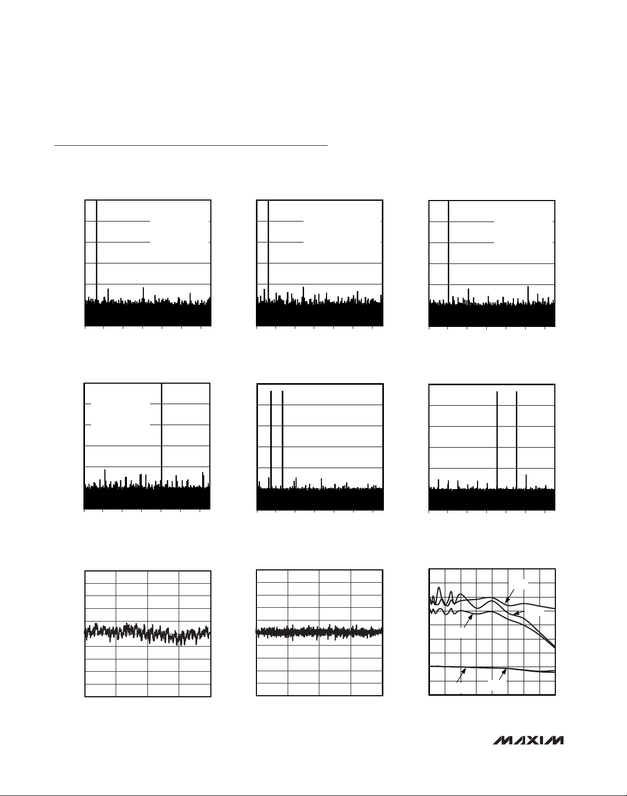
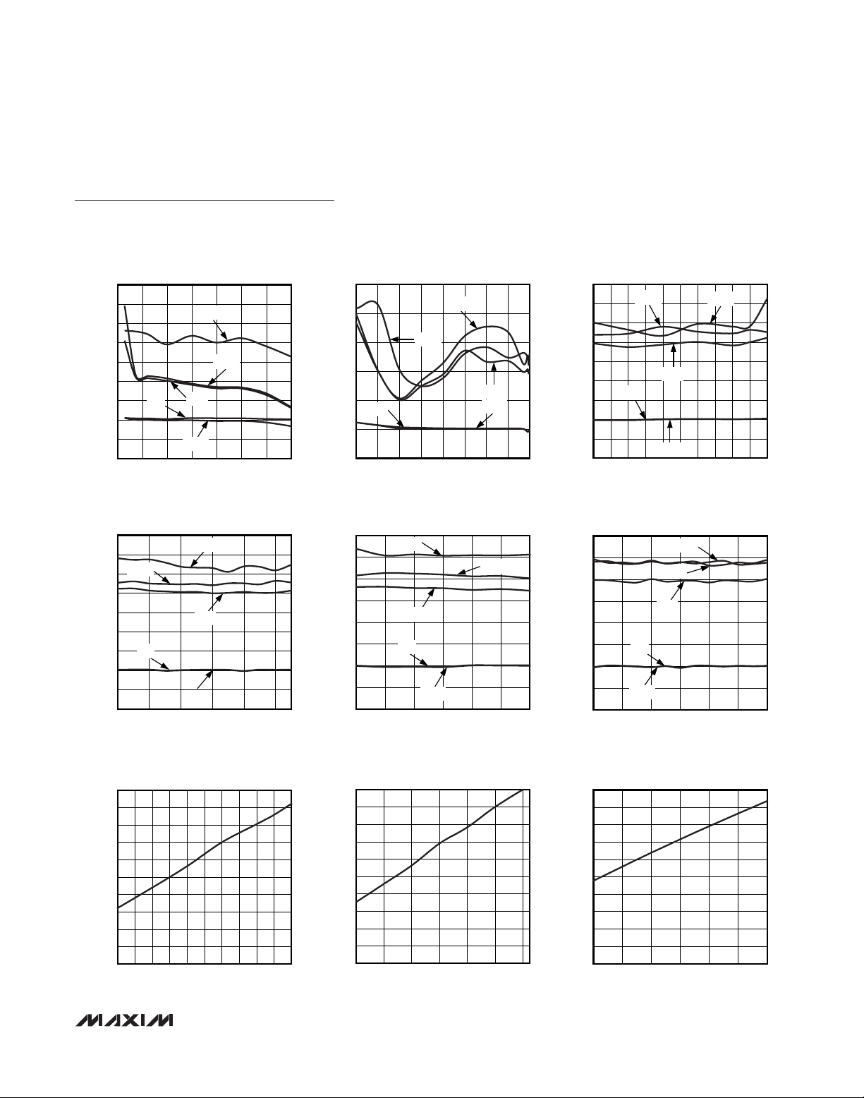
175MHz TWO-TONE IMD
FREQUENCY (MHz)
AMPLITUDE (dBFS)
MAX19515 toc06
-120
-100
-80
-60
-40
-20
0
f
IN1
= 172.49286MHz
f
IN2
= 177.50202MHz
0 5 10 15 25 3020
70MHz TWO-TONE IMD PLOT
FREQUENCY (MHz)
AMPLITUDE (dBFS)
MAX19515 toc05
-120
-100
-80
-60
-40
-20
0
f
IN1
= 71.496925MHz
f
IN2
= 68.504600MHz
0 5 10 15 25 3020
175MHz INPUT FFT PLOT
FREQUENCY (MHz)
AMPLITUDE (dBFS)
MAX19515 toc04
-120
-100
-80
-60
-40
-20
0
0 5 10 15 25 3020
fIN = 175.096626MHz
A
IN
= -0.512dBFS
SNR = 59.073dB
SINAD = 59.022dB
THD = -78.338dBc
SFDR1 = 81.806dBc
SFDR2 = 84.255dBc
70MHz INPUT FFT PLOT
FREQUENCY (MHz)
AMPLITUDE (dBFS)
MAX19515 toc03
-120
-100
-80
-60
-40
-20
0
0 5 10 15 25 3020
fIN = 70.1014328MHz
A
IN
= -0.532dBFS
SNR = 59.432dB
SINAD = 58.388dB
THD = -79.349dBc
SFDR1 = 84.227dBc
SFDR2 = 81.877dBc
3MHz SINGLE-ENDED INPUT FFT PLOT
FREQUENCY (MHz)
AMPLITUDE (dBFS)
MAX19515 toc02
-120
-100
-80
-60
-40
-20
0
0 5 10 15 25 3020
fIN = 2.99877166748047MHz
A
IN
= -0.546dBFS
SNR = 59.675dB
SINAD = 59.632dB
THD = -79.673dBc
SFDR1 = 88.737dBc
SFDR2 = 82.290dBc
MAX19515
Dual-Channel, 10-Bit, 65Msps ADC
8 _______________________________________________________________________________________
Typical Operating Characteristics
(V
AVDD
= V
OVDD
= 1.8V, internal reference, differential clock, V
CLK
= 1.5V
P-P
, f
CLK
= 65MHz, AIN= -0.5dBFS, data output termination
= 50Ω, T
A
= +25°C, unless otherwise noted.)
3MHz INPUT FFT PLOT
FREQUENCY (MHz)
AMPLITUDE (dBFS)
MAX19515 toc01
0 5 10 15 25 3020
-120
-100
-80
-60
-40
-20
0
fIN = 2.99877166MHz
A
IN
= -0.532dBFS
SNR = 59.682dB
SINAD = 59.641dB
THD = -79.826dBc
SFDR1 = 83.946dBc
SFDR2 = 82.852dBc
INTEGRAL NONLINEARITY
vs. DIGITAL OUTPUT CODE
DIGITAL OUTPUT CODE
INL (LSB)
MAX19515 toc07
0 256 512 768 1024
-1.0
-0.8
-0.6
-0.4
-0.2
0
0.2
0.4
0.6
0.8
1.0
DIFFERENTIAL NONLINEARITY
vs. DIGITAL OUTPUT CODE
DIGITAL OUTPUT CODE
DNL (LSB)
MAX19515 toc08
0 256 512 768 1024
-1.0
-0.8
-0.6
-0.4
-0.2
0
0.2
0.4
0.6
0.8
1.0
PERFORMANCE vs. INPUT FREQUENCY
INPUT FREQUENCY (MHz)
PERFORMANCE (dBFS)
MAX19515 toc09
0 50 100 150 200 250 300 350 400
50
55
60
65
70
75
80
85
90
95
-THD
SINAD
SFDR1
SNR
SFDR2
Page 9
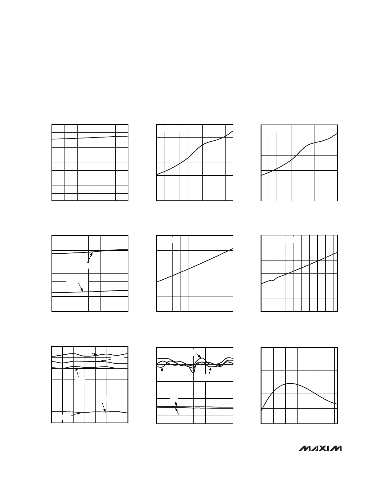
ANALOG SUPPLY CURRENT
vs. SUPPLY VOLTAGE
SUPPLY VOLTAGE (V)
ANALOG SUPPLY CURRENT (mA)
MAX19515 toc18
1.65 1.70 1.75 1.80 1.85 1.90 1.95
40
41
42
43
44
45
46
47
48
49
50
PERFORMANCE
vs. ANALOG INPUT AMPLITUDE
ANALOG INPUT AMPLITUDE (dBFS)
PERFORMANCE (dBFS)
MAX19515 toc11
-80 -70 -60 -50 -40 -30 -20 -10 0
50
60
70
80
90
100
110
SFDR2
SFDR1
-THD
SINAD
SNR
SINGLE-ENDED PERFORMANCE
vs. INPUT FREQUENCY
INPUT FREQUENCY (MHz)
SINGLE-ENDED PERFORMANCE (dBFS)
MAX19515 toc10
0 10203040506070
50
55
60
65
70
75
80
85
90
95
SFDR2
SFDR1
-THD
SINAD
SNR
Typical Operating Characteristics (continued)
(V
AVDD
= V
OVDD
= 1.8V, internal reference, differential clock, V
CLK
= 1.5V
P-P
, f
CLK
= 65MHz, AIN= -0.5dBFS, data output termination
= 50Ω, T
A
= +25°C, unless otherwise noted.)
MAX19515
Dual-Channel, 10-Bit, 65Msps ADC
_______________________________________________________________________________________
9
PERFORMANCE
vs. COMMON-MODE VOLTAGE
95
90
SFDR2
85
80
75
70
SNR
65
PERFORMANCE (dBFS)
60
55
50
0.35 0.55 0.75 0.95 1.15 1.35
COMMON-MODE VOLTAGE (V)
SFDR1
-THD
SINAD
90
85
MAX19515 toc13
80
75
70
65
PERFORMANCE (dBFS)
60
55
50
PERFORMANCE
vs. ANALOG SUPPLY VOLTAGE
SFDR2
-THD
SNR
SINAD
1.65 1.70 1.75 1.80 1.85 1.90 1.95
ANALOG SUPPLY VOLTAGE (V)
PERFORMANCE
vs. SAMPLING FREQUENCY
95
90
85
80
75
70
65
PERFORMANCE (dBFS)
60
55
50
20 25 30 35 40 45 50 55 60 65 70
SFDR2
-THD
SNR
SINAD
SAMPLING FREQUENCY (Msps)
PERFORMANCE
vs. ANALOG SUPPLY VOLTAGE
SFDR1
90
85
MAX19515 toc14
80
75
70
65
PERFORMANCE (dBFS)
60
55
50
2.3 2.5 2.7 2.9 3.1 3.3 3.5
ANALOG SUPPLY VOLTAGE (V)
SFDR2
SFDR1
-THD
SNR
SINAD
SFDR1
MAX19515 toc12
MAX19515 toc15
ANALOG SUPPLY CURRENT
vs. SAMPLING FREQUENCY
50
48
46
44
42
40
38
36
34
ANALOG SUPPLY CURRENT (mA)
32
30
20 25 30 35 40 45 50 55 60 65 70
SAMPLING FREQUENCY (MHz)
ANALOG SUPPLY CURRENT
vs. TEMPERATURE
50
49
MAX19515 toc17
48
MAX19515 toc16
47
46
45
44
43
42
ANALOG SUPPLY CURRENT (mA)
41
40
-40 -20 0 20 40 60 80
TEMPERATURE (°C)
Page 10
10 ______________________________________________________________________________________
Typical Operating Characteristics (continued)
(V
AVDD
= V
OVDD
= 1.8V, internal reference, differential clock, V
CLK
= 1.5V
P-P
, f
CLK
= 65MHz, AIN= -0.5dBFS, data output termination
= 50Ω, T
A
= +25°C, unless otherwise noted.)
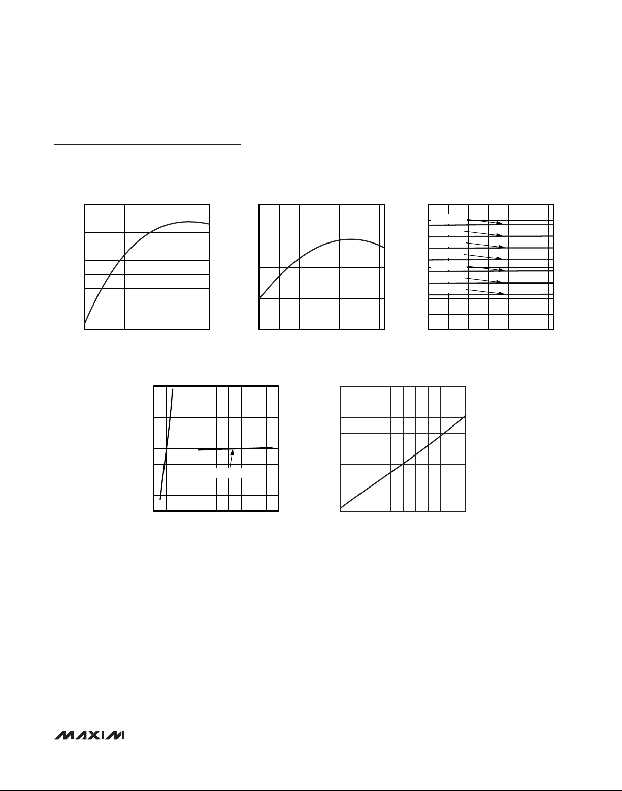
ANALOG SUPPLY CURRENT
vs. SUPPLY VOLTAGE
SUPPLY VOLTAGE (V)
ANALOG SUPPLY CURRENT (mA)
MAX19515 toc19
2.3 2.5 2.7 2.9 3.1 3.3 3.5
40
41
42
43
44
45
46
47
48
49
50
MAX19515
Dual-Channel, 10-Bit, 65Msps ADC
DIGITAL SUPPLY CURRENT
25
23
21
19
17
15
13
11
SUPPLY CURRENT (mA)
9
7
5
-40-200 20406080
vs. TEMPERATURE
V
= 3.6V
OVDD
V
= 1.8V
OVDD
TEMPERATURE (°C)
12
V
OVDD
10
8
6
4
DIGITAL SUPPLY CURRENT (mA)
2
0
20 25 30 35 40 45 50 55 60 65 70
25
DUAL BUS
MAX19515 toc22
20
15
10
5
DIGITAL SUPPLY CURRENT (mA)
0
1.7 1.9 2.1 2.3 2.5 2.7 2.9 3.1 3.3 3.5
DIGITAL SUPPLY CURRENT
vs. SAMPLING FREQUENCY
= 1.8V
SAMPLING FREQUENCY (Msps)
DIGITAL SUPPLY CURRENT
vs. SUPPLY VOLTAGE
SUPPLY VOLTAGE (V)
25
V
OVDD
MAX19515 toc20
20
15
10
5
DIGITAL SUPPLY CURRENT (mA)
0
20 25 30 35 40 45 50 55 60 65 70
30
MULTIPLEXED BUS
25
MAX19515 toc23
20
15
10
DIGITAL SUPPLY CURRENT (mA)
5
0
1.7 1.9 2.1 2.3 2.5 2.7 2.9 3.1 3.3 3.5
DIGITAL SUPPLY CURRENT
vs. SAMPLING FREQUENCY
= 3.6V
MAX19515 toc21
SAMPLING FREQUENCY (Msps)
DIGITAL SUPPLY CURRENT
vs. SUPPLY VOLTAGE
MAX19515 toc24
SUPPLY VOLTAGE (V)
90
vs. CLOCK DUTY CYCLE
85
80
75
70
PERFORMANCE (dBFS)
65
60
SINAD
55
30 35 40 45 50 55 60 65
CLOCK DUTY CYCLE (%)
PERFORMANCE
SFDR1
-THD
SNR
SFDR2
95
90
MAX19515 toc25
85
80
75
70
65
PERFORMANCE (dBFS)
60
55
50
PERFORMANCE vs. TEMPERATURE
SFDR1
SFDR2
SNR
SINAD
-40 -20 0 20 40 60 80
TEMPERATURE (°C)
-THD
MAX19515 toc26
GAIN ERROR vs. TEMPERATURE
0.05
0.04
0.03
0.02
0.01
0
-0.01
GAIN ERROR (%)
-0.02
-0.03
-0.04
-0.05
-40-200 20406080
TEMPERATURE (°C)
MAX19515 toc27
Page 11
Typical Operating Characteristics (continued)
(V
AVDD
= V
OVDD
= 1.8V, internal reference, differential clock, V
CLK
= 1.5V
P-P
, f
CLK
= 65MHz, AIN= -0.5dBFS, data output termination
= 50Ω, T
A
= +25°C, unless otherwise noted.)
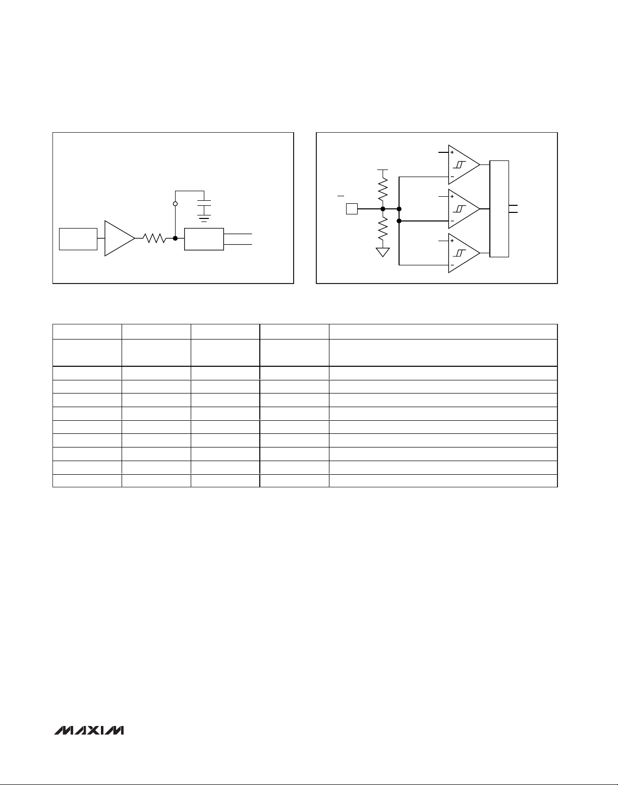
COMMON-MODE REFERENCE VOLTAGE
vs. TEMPERATURE
TEMPERATURE (°C)
COMMON-MODE REFERENCE VOLTAGE (V)
MAX19515 toc30
-40-200 20406080
0
0.2
0.4
0.6
0.8
1.0
1.2
1.4
1.6
VCM = 1.2V
VCM = 1.05V
VCM = 0.9V
VCM = 0.75V
VCM = 0.6V
VCM = 0.45V
VCM = 1.35V
OFFSET ERROR vs. TEMPERATURE
TEMPERATURE (°C)
OFFSET ERROR (mV)
MAX19515 toc28
-40-200 20406080
-0.7
-0.6
-0.5
-0.4
-0.3
-0.2
-0.1
0
0.1
0.2
MAX19515
Dual-Channel, 10-Bit, 65Msps ADC
______________________________________________________________________________________
11
GAIN ERROR vs. SUPPLY VOLTAGE
0.08
0.06
0.04
0.02
0
-0.02
GAIN ERROR (%)
-0.04
-0.06
-0.08
1.6 1.8 2.0 2.2 2.4 2.6 2.8 3.0 3.2 3.4 3.6
SUPPLY VOLTAGE (V)
1.2516
1.2495
1.2474
REFERENCE VOLTAGE (V)
1.2453
1.2432
REGULATOR MODE
REFERENCE VOLTAGE
vs. TEMPERATURE
-40-200 20406080
TEMPERATURE (°C)
INPUT CURRENT
vs. COMMON-MODE VOLTAGE
60
MAX19515 toc31
55
50
45
40
35
INPUT CURRENT (µA)
30
25
20
0.4 0.5 0.6 0.7 0.8 0.9 1.0 1.1 1.2 1.3 1.4
COMMON-MODE VOLTAGE (V)
MAX19515 toc29
MAX19515 toc32
Page 12

MAX19515
Dual-Channel, 10-Bit, 65Msps ADC
12 ______________________________________________________________________________________
Pin Description
PIN NAME FUNCTION
1, 12, 13, 48 AVDD Analog Supply Voltage. Bypass each AVDD input pair (1, 48) and (12, 13) to GND with 0.1µF.
2 CMA Channel A Common-Mode Input-Voltage Reference
3 INA+ Channel A Positive Analog Input
4 INA- Channel A Negative Analog Input
5 SPEN Active-Low SPI Enable. Drive high to enable parallel programming mode.
6 REFIO
7 SHDN
8 I.C. Internally Connected. Leave unconnected.
9 INB+ Channel B Positive Analog Input
10 INB- Channel B Negative Analog Input
11 CMB Channel B Common-Mode Input-Voltage Reference
14 SYNC Clock-Divider Mode Synchronization Input
15 CLK+ Clock Positive Input
16 CLK-
17, 18 GND Ground. Connect all ground inputs and EP (exposed pad) together.
19 DORB Channel B Data Over Range
20 DCLKB Channel B Data Clock
21 D0B Channel B Three-State Digital Output, Bit 0 (LSB)
22 D1B Channel B Three-State Digital Output, Bit 1
23 D2B Channel B Three-State Digital Output, Bit 2
24 D3B Channel B Three-State Digital Output, Bit 3
25, 36 OVDD Digital Supply Voltage. Bypass each OVDD input to GND with 0.1µF capacitor.
26 D4B Channel B Three-State Digital Output, Bit 4
27 D5B Channel B Three-State Digital Output, Bit 5
28 D6B Channel B Three-State Digital Output, Bit 6
29 D7B Channel B Three-State Digital Output, Bit 7
30 D8B Channel B Three-State Digital Output, Bit 8
31 D9B Channel B Three-State Digital Output, Bit 9 (MSB)
32 D0A Channel A Three-State Digital Output, Bit 0 (LSB)
33 D1A Channel A Three-State Digital Output, Bit 1
34 D2A Channel A Three-State Digital Output, Bit 2
35 D3A Channel A Three-State Digital Output, Bit 3
37 D4A Channel A Three-State Digital Output, Bit 4
38 D5A Channel A Three-State Digital Output, Bit 5
39 D6A Channel A Three-State Digital Output, Bit 6
Reference Input/Output. To use internal reference, bypass to GND with a > 0.1µF capacitor. See
the Reference Input/Output (REFIO) section for external reference adjustment.
Active-High Power-Down. If SPEN is high (parallel programming mode), a register reset is initiated
on the falling edge of SHDN.
Clock Negative Input. If CLK- is connected to ground, CLK+ is a single-ended logic-level clock
input. Otherwise, CLK+/CLK- are self-biased differential clock inputs.
Page 13

MAX19515
Dual-Channel, 10-Bit, 65Msps ADC
______________________________________________________________________________________ 13
Detailed Description
The MAX19515 uses a 10-stage, fully differential,
pipelined architecture (Figure 1) that allows for highspeed conversion while minimizing power consumption. Samples taken at the inputs move progressively
through the pipeline stages every half clock cycle.
From input to output the total latency is 9 clock cycles.
Each pipeline converter stage converts its input voltage
to a digital output code. At every stage, except the last,
the error between the input voltage and the digital output code is multiplied and passed on to the next
pipeline stage. Digital error correction compensates for
ADC comparator offsets in each pipeline stage and
ensures no missing codes. Figure 2 shows the
MAX19515 functional diagram.
Analog Inputs and Common-Mode
Reference
Apply the analog input signal to the analog inputs
(INA+/INA- or INB+/INB-), which are connected to the
input sampling switch (Figure 3). When the input sampling switch is closed, the input signal is applied to the
sampling capacitors through the input switch resistance.
The input signal is sampled at the instant the input
switch opens. The pipeline ADC processes the sampled
voltage and the digital output result is available 9 clock
cycles later. Before the input switch is closed to begin
the next sampling cycle, the sampling capacitors are
reset to the input common-mode potential.
Common-mode bias can be provided externally or
internally through 2kΩ resistors. In DC-coupled applications, the signal source provides the external bias and
the bias current. In AC-coupled applications, the input
current is supplied by the common-mode input voltage.
For example, the input current can be supplied through
the center tap of a transformer secondary winding.
Alternatively, program the appropriate internal register
through the serial-port interface to supply the input DC
current through internal 2kΩ resistors (Figure 3). When
the input current is supplied through the internal resistors, the input common-mode potential is reduced by
the voltage drop across the resistors. The commonmode input reference voltage can be adjusted through
programmable register settings from 0.45V to 1.35V in
0.15V increments. The default setting is 0.90V. Use this
feature to provide a common-mode output reference to
a DC-coupled driving circuit.
Pin Description (continued)
Figure 1. Pipeline Architecture—Stage Blocks
PIN NAME FUNCTION
40 D7A Channel A Three-State Digital Output, Bit 7
41 D8A Channel A Three-State Digital Output, Bit 8
42 D9A Channel A Three-State Digital Output, Bit 9 (MSB)
43 DORA Channel A Data Over Range
44 DCLKA Channel A Data Clock
45 SDIN/FORMAT SPI Data Input/Format. Serial-data input when SPEN is low. Output data format when SPEN is high.
46 SCLK/DIV Serial Clock/Clock Divider. Serial clock when SPEN is low. Clock divider when SPEN is high.
47 CS/OUTSEL
—EP
Serial-Port Select/Data Output Mode. Serial-port select when SPEN is low. Data output mode
selection when SPEN is high.
Exposed Pad. Internally connected to GND. Connect to a large ground plane to maximize thermal
performance.
IN_+
IN_-
MAX19515
FLASH
ADC
STAGE 1 STAGE 9
STAGE 2
DIGITAL ERROR CORRECTION
+
Σ
−
DAC
D0_ THROUGH D9_
x2
STAGE 10
END OF PIPELINE
Page 14

MAX19515
Dual-Channel, 10-Bit, 65Msps ADC
14 ______________________________________________________________________________________
Figure 2. Functional Diagram
Figure 3. Internal Track-and-Hold (T/H) Circuit
CLOCK
MAX19515
INA+
INA-
CMA
REFIO
CMB
INB+
INB-
T/H
T/H
PIPELINE
ADC
REFERENCE
AND BIAS
SYSTEM
PIPELINE
ADC
DIGITAL
ERROR
CORRECTION
INTERNAL
REFERENCE
GENERATOR
DIGITAL
ERROR
CORRECTION
DATA
AND
OUTPUT
FORMAT
CLOCK
OUTPUT
DRIVERS
D0A–D9A
DORA
DCLKA
OVDD
(1.8V TO 3.3V)
D0B–D9B
DORB
DCLKB
CLK+
CLK-
SYNC
CS
SCLK
SDIN
SPEN
CMA
INA+
INA-
2kΩ
2kΩ
CLOCK
DIVIDER
SERIAL PORT
AND
CONTROL REGISTERS
DUTY-
CYCLE
EQUALIZER
1.8V INTERNAL
INTERNAL CONTROL
AVDD
*V
COM
AVDD
C
PAR
0.7pF
C
PAR
0.7pF
REGULATOR
AND
POWER CONTROL
R
SWITCH
120Ω
R
SWITCH
120Ω
C
SAMPLE
1.2pF
C
SAMPLE
1.2pF
AVDD
(1.8V OR
2.5V TO 3.3V)
SHDN
GND
SAMPLING CLOCK
*V
PROGRAMMABLE FROM 0.45V TO 1.35V. SEE COMMON-MODE REGISTER (08h)
COM
MAX19515
Page 15
MAX19515
Dual-Channel, 10-Bit, 65Msps ADC
______________________________________________________________________________________ 15
Reference Input/Output (REFIO)
REFIO adjusts the reference potential, which, in turn,
adjusts the full-scale range of the ADC. Figure 4 shows
a simplified schematic of the reference system. An
internal bandgap voltage generator provides an internal
reference voltage. The bandgap potential is buffered
and applied to REFIO through a 10kΩ resistor. Bypass
REFIO with a 0.1µF capacitor to GND. The bandgap
voltage is applied to a scaling and level-shift circuit,
which creates internal reference potentials that establish the full-scale range of the ADC. Apply an external
voltage on REFIO to trim the ADC full scale. The allowable adjustment range is +5/-15%. The REFIO-to-ADC
gain transfer function is:
VFS= 1.5 x [V
REFIO
/1.25] Volts
Programming and Interface
There are two ways to control the MAX19515 operating
modes. Full feature selection is available using the SPI
interface, while the parallel interface offers a limited set
of commonly used features. The programming mode is
selected using the SPEN input. Drive SPEN low for SPI
interface; drive SPEN high for parallel interface.
Parallel Interface
The parallel interface offers a pin-programmable interface with a limited feature set. Connect SPEN to AVDD
to enable the parallel interface. See Table 1 for pin
functionality; see Figure 5 for a simplified parallel-interface input schematic.
BANDGAP
REFERENCE
BUFFER
1.250V
REFIO
INTERNAL GAIN—BYPASS REFIO
EXTERNAL GAIN CONTROL—DRIVE REFIO
SCALE AND
LEVEL SHIFT
INTERNAL REFERENCE
(CONTROLS ADC GAIN)
10kΩ
0.1µF
EXTERNAL BYPASS
Figure 4. Simplified Reference Schematic
36kΩ
156kΩ
CS
SCLK
SDIN
AVDD
29/32 AVDD
DECODER
TO
CONTROL
LOGIC
23/32 AVDD
3/32 AVDD
Figure 5. Simplified Parallel-Interface Input Schematic
Table 1. Parallel-Interface Pin Functionality
X = Don’t care.
SPEN SDIN/FORMAT SCLK/DIV CS/OUTSEL DESCRIPTION
0 SDIN SCLK CS
1 0 X X Two’s complement
1 AVDD X X Offset binary
1 Unconnected X X Gray code
1 X 0 X Clock divide-by-1
1 X AVDD X Clock divide-by-2
1 X Unconnected X Clock divide-by-4
1 X X 0 CMOS (dual bus)
1 X X AVDD MUX CMOS (channel A data bus)
1 X X Unconnected MUX CMOS (channel B data bus)
SPI interface active. Features are programmed through the
serial port (see the Serial Programming Interface section).
Page 16
MAX19515
Dual-Channel, 10-Bit, 65Msps ADC
16 ______________________________________________________________________________________
Serial Programming Interface
A serial interface programs the MAX19515 control registers through the CS, SDIN, and SCLK inputs. Serial
data is shifted into SDIN on the rising edge of SCLK
when CS is low. The MAX19515 ignores the data presented at SDIN and SCLK when CS is high.
CCSS
must
transition high after each read/write operation. SDIN
also serves as the serial-data output for reading control
registers. The serial interface supports two-byte transfer
in a communication cycle. The first byte is a control
byte, containing the address and read/write instruction,
written to the MAX19515. The second byte is a data
byte and can be written to or read from the MAX19515.
Figure 6 shows a serial-interface communication cycle.
The first SDIN bit clocked in establishes the communi-
cation cycle as either a write or read transaction (0 for
write operation and 1 for read operation). The following
7 bits specify the address of the register to be written or
read. The final 8 SDIN bits are the register data. All
address and data bits are clocked in or out MSB first.
During a read operation, the MAX19515 serial port drives read data (D7) into SDIN after the falling edge of
SCLK following the 8th rising edge of SCLK. Since the
minimum hold time on SDIN input is zero, the master
can stop driving SDIN any time after the 8th rising edge
of SCLK. Subsequent data bits are driven into SDIN on
the falling edge of SCLK. Output data in a read operation is latched on the rising edge of SCLK. Figure 7
shows the detailed serial-interface timing diagram.
R/W A6 A4A5 A2A3 A0A1 D7 D6 D4D5 D2D3 D0D1
R/W
0 = WRITE
1 = READ
CS
SCLK
SDIN
ADDRESS
DATA
WRITE OR READ
CS
t
CSS
t
CSH
t
SDD
t
SDS
t
SDH
t
SCLK
SCLK
SDIN
WRITE READ
Figure 6. Serial-Interface Communication Cycle
Figure 7. Serial-Interface Timing Diagram
Page 17
MAX19515
Dual-Channel, 10-Bit, 65Msps ADC
______________________________________________________________________________________ 17
Table 2. Register 0Ah Status Byte
Table 3. User-Programmable Registers
Register address 0Ah is a special-function register.
Writing data 5Ah to register 0Ah initiates a register
reset. When this operation is executed, all control regis-
ters are reset to default values. A read operation of register 0Ah returns a status byte with information
described in Table 2.
The SHDN input (pin 7) toggles between any two
power-management states. The Power Management
register defines each power-management state. In the
default state, SHDN = 1 shuts down the MAX19515 and
SHDN = 0 returns to full power.
User-Programmable Registers
Power Management (00h)
BIT NO. VALUE DESCRIPTION
7 0 Reserved
6 0 Reserved
5 0 or 1 1 = ROM read in progress
4 0 or 1 1 = ROM read completed and register data is valid (checksum is OK)
3 0 Reserved
2 1 Reserved
1 0 or 1 Reserved
0 0 or 1 1 = Duty-cycle equalizer DLL is locked
ADDRESS POR DEFAULT FUNCTION
00h 00000011 Power management
01h 00000000 Output format
02h 00000000 Digital output power management
03h 10000000 Data/DCLK timing
04h 00000000 C H A d ata outp ut ter m i nati on contr ol
05h 00000000 C H B d ata outp ut ter m i nati on contr ol
06h 00000000 C l ock d i vi d e/d ata for m at/test p atter n
07h Reserved Reserved—do not use
08h 00000000 Common mode
0Ah — Software reset
BIT 7 BIT 6 BIT 5 BIT 4 BIT 3 BIT 2 BIT 1 BIT 0
HPS_SHDN1 STBY_SHDN1 C H B_ON _S H D N 1C H A_O N _S H D N 1 HPS_SHDN0 STBY_SHDN0 CHB_ON_SHDN0 C H A_O N _S H D N 0
Page 18
MAX19515
Dual-Channel, 10-Bit, 65Msps ADC
18 ______________________________________________________________________________________
Control Bits:
Output Format (01h)
In addition to power management, the HPS_SHDN1
and HPS_SHDN0 activate an A+B adder mode. In this
mode, the results from both channels are averaged.
The MUX_CH bit selects which bus the (A+B)/2 data is
presented.
*
HPS_SHDN0, STBY_SHDN0, CHA_ON_SHDN0, and CHB_ON_SHDN0 are active when SHDN = 0.
**
HPS_SHDN1, STBY_SHDN1, CHA_ON_SHDN1, and CHB_ON_SHDN1 are active when SHDN = 1.
X = Don’t care.
Note: When HPS_SHDN_ = 1 (A+B adder mode), CHA_ON_SHDN_ and CHB_ON_SHDN_ must BOTH equal 0 for power-down or
standby.
Bit 7, 6, 5 Set to 0 for proper operation
Bit 4 BIT_ORDER_B: Reverse CHB output bit order
0 = Defined data bus pin order (default)
1 = Reverse data bus pin order
Bit 3 BIT_ORDER_A: Reverse CHA output bit order
0 = Defined data bus pin order (default)
1 = Reverse data bus pin order
Bit 2 MUX_CH: Multiplexed data bus selection
0 = Multiplexed data output on CHA (CHA data presented first, followed by CHB data) (default)
1 = Multiplexed data output on CHB (CHB data presented first, followed by CHA data)
Bit 1 MUX: Digital output mode
0 = Dual data bus output mode (default)
1 = Single multiplexed data bus output mode
MUX_CH selects the output bus
Bit 0 Set to 0 for proper operation
HPS_SHDN0 STBY_SHDN0 CHA_ON_SHDN0 CHB_ON_SHDN0 SHDN INPUT = 0*
HPS_SHDN1 STBY_SHDN1 CHA_ON_SHDN1 CHB_ON_SHDN1 SHDN INPUT = 1**
X 0 0 0 Complete power-down
0 0 0 1 Channel B active, channel A full power-down
0 0 1 0 Channel A active, channel B full power-down
0 X 1 1 Channels A and B active
0 1 0 0 Channels A and B in standby mode
0 1 0 1 Channel B active, channel A standby
0 1 1 0 Channel A active, channel B standby
1 1 0 0 Channels A and B in standby mode
1 X X 1 Channels A and B active, output is averaged
1 X 1 X Channels A and B active, output is averaged
BIT 7 BIT 6 BIT 5 BIT 4 BIT 3 BIT 2 BIT 1 BIT 0
0 0 0 BIT_ORDER_B BIT_ORDER_A MUX_CH MUX 0
Page 19

MAX19515
Dual-Channel, 10-Bit, 65Msps ADC
______________________________________________________________________________________ 19
Digital Output Power Management (02h)
Bit 7–4 Don’t care
Bit 3, 2 PD_DOUT_1, PD_DOUT_0: Power-down digital output state control
00 = Digital output three state (default)
01 = Digital output low
10 = Digital output three state
11 = Digital output high
Bit 1 DIS_DOR: DOR driver disable
0 = DOR active (default)
1 = DOR disabled (three state)
Bit 0 DIS_DCLK: DCLK driver disable
0 = DCLK active (default)
1 = DCLK disabled (three state)
BIT 7 BIT 6 BIT 5 BIT 4 BIT 3 BIT 2 BIT 1 BIT 0
X X X X PD_DOUT_1 PD_DOUT_0 DIS_DOR DIS_DCLK
Page 20
MAX19515
Dual-Channel, 10-Bit, 65Msps ADC
20 ______________________________________________________________________________________
Data/DCLK Timing (03h)
Bit 7 DA_BYPASS: Data aligner bypass
0 = Nominal
1 = Bypasses data aligner delay line to minimize output data latency with respect to the input clock.
Rising clock to data transition is approximately 6ns with DTIME = 000b settings (default)
Bit 6 DLY_HALF_T: Data and DCLK delayed by T/2
0 = Normal, no delay (default)
1 = Delays data and DCLK outputs by T/2
Disabled in MUX data bus mode
Bit 5, 4, 3 DCLKTIME_2, DCLKTIME_1, DCLKTIME_0: DCLK timing adjust (controls both channels)
000 = Nominal (default)
001 = +T/16
010 = +2T/16
011 = +3T/16
100 = Reserved, do not use
101 = -1T/16
110 = -2T/16
111 = -3T/16
Bit 2, 1, 0 DTIME_2, DTIME_1, DTIME_0: Data timing adjust (controls both channels)
000 = Nominal (default)
001 = +T/16
010 = +2T/16
011 = +3T/16
100 = Reserved, do not use
101 = -1T/16
110 = -2T/16
111 = -3T/16
BIT 7 BIT 6 BIT 5 BIT 4 BIT 3 BIT 2 BIT 1 BIT 0
DA_BYPASS DLY_HALF_T DCLKTIME_2 DCLKTIME_1 DCLKTIME_0 DTIME_2 DTIME_1 DTIME_0
Page 21
MAX19515
Dual-Channel, 10-Bit, 65Msps ADC
______________________________________________________________________________________ 21
CHA Data Output Termination Control (04h)
Bit 7, 6 Don’t care
Bit 5, 4, 3 CT_DCLK_2_A, CT_DCLK_1_A, CT_DCLK_0_A: CHA DCLK termination control
000 = 50Ω (default)
001 = 75Ω
010 = 100Ω
011 = 150Ω
1xx = 300Ω
Bit 2, 1, 0 CT_DATA_2_A, CT_DATA_1_A, CT_DATA_0_A: CHA data output termination control
000 = 50Ω (default)
001 = 75Ω
010 = 100Ω
011 = 150Ω
1xx = 300Ω
CHB Data Output Termination Control (05h)
Bit 7, 6 Don’t care
Bit 5, 4, 3 CT_DCLK_2_B, CT_DCLK_1_B, CT_DCLK_0_B: CHB DCLK termination control
000 = 50Ω (default)
001 = 75Ω
010 = 100Ω
011 = 150Ω
1xx = 300Ω
Bit 2, 1, 0 CT_DATA_2_B, CT_DATA_1_B, CT_DATA_0_B: CHB data output termination control
000 = 50Ω (default)
001 = 75Ω
010 = 100Ω
011 = 150Ω
1xx = 300Ω
BIT 7 BIT 6 BIT 5 BIT 4 BIT 3 BIT 2 BIT 1 BIT 0
X X CT_DCLK_2_A CT_DCLK_1_A CT_DCLK_0_A CT_DATA_2_A CT_DATA_1_A CT_DATA_0_A
BIT 7 BIT 6 BIT 5 BIT 4 BIT 3 BIT 2 BIT 1 BIT 0
X X CT_DCLK_2_B CT_DCLK_1_B CT_DCLK_0_B CT_DATA_2_B CT_DATA_1_B CT_DATA_0_B
Page 22

MAX19515
Dual-Channel, 10-Bit, 65Msps ADC
22 ______________________________________________________________________________________
Clock Divide/Data Format/Test Pattern (06h)
Reserved (07h)—Do not write to this register
Bit 7 TEST_PATTERN: Test pattern selection
0 = Ramps from 0 to 1023 (offset binary) and repeats (subsequent formatting applied) (default)
1 = Data alternates between D[9:0] = 0101010101, DOR = 1, and D[9:0] = 1010101010,
DOR = 0 on both channels
Bit 6 TEST_DATA: Data test mode
0 = Normal data output (default)
1 = Outputs test data pattern
Bit 5, 4 FORMAT_1, FORMAT_0: Data numerical format
00 = Two’s complement (default)
01 = Offset binary
10 = Gray code
11 = Two’s complement
Bit 3 TERM_100: Select 100Ω clock input termination
0 = No termination (default)
1 = 100Ω termination across differential clock inputs
Bit 2 SYNC_MODE: Divider synchronization mode select
0 = Slip mode (Figure 11) (default)
1 = Edge mode (Figure 12)
Bit 1, 0 DIV1, DIV0: Input clock-divider select
00 = No divider (default)
01 = Divide-by-2
10 = Divide-by-4
11 = No divider
BIT 7 BIT 6 BIT 5 BIT 4 BIT 3 BIT 2 BIT 1 BIT 0
TEST_PATTERN TEST_DATA FORMAT_1 FORMAT_0 TERM_100 SYNC_MODE DIV1 DIV0
Page 23

MAX19515
Dual-Channel, 10-Bit, 65Msps ADC
______________________________________________________________________________________ 23
Common Mode (08h)
Software Reset (0Ah)
Bit 7 CMI_SELF_B: CHB connect input common-mode to analog inputs
0 = Internal common-mode voltage is NOT applied to inputs (default)
1 = Internal common-mode voltage applied to analog inputs through 2kΩ resistors
Bit 6, 5, 4 CMI_ADJ_2_B, CMI_ADJ_1_B, CMI_ADJ_0_B: CHB input common-mode voltage adjustment
000 = 0.900V (default)
001 = 1.050V
010 = 1.200V
011 = 1.350V
100 = 0.900V
101 = 0.750V
110 = 0.600V
111 = 0.450V
Bit 3 CMI_SELF_A: CHA connect input common-mode to analog inputs
0 = Internal common-mode voltage is NOT applied to inputs (default)
1 = Internal common-mode voltage applied to analog inputs through 2kΩ resistors
Bit 2, 1, 0 CMI_ADJ_2_A, CMI_ADJ_1_A, CMI_ADJ_0_A: CHA input common-mode adjustment
000 = 0.900V (default)
001 = 1.050V
010 = 1.200V
011 = 1.350V
100 = 0.900V
101 = 0.750V
110 = 0.600V
111 = 0.450V
Bit 7–0 SWRESET: Write 5Ah to initiate software reset
BIT 7 BIT 6 BIT 5 BIT 4 BIT 3 BIT 2 BIT 1 BIT 0
CMI_SELF_B CMI_ADJ_2_B CMI_ADJ_1_B CMI_ADJ_0_B CMI_SELF_A CMI_ADJ_2_A CMI_ADJ_1_A CMI_ADJ_0_A
Page 24

Clock Inputs
The input clock interface provides for flexibility in the
requirements of the clock driver. The MAX19515
accepts a fully differential clock or single-ended logiclevel clock. For differential clock operation, connect a
differential clock to the CLK+ and CLK- inputs. In this
mode, the input common mode is established internally
to allow for AC-coupling. The differential clock signal
can also be DC-coupled if the common mode is constrained to the specified 1V to 1.4V clock input common-mode range. For single-ended operation, connect
CLK- to GND and drive the CLK+ input with a logiclevel signal. When the CLK- input is grounded (or
pulled below the threshold of the clock mode detection
comparator) the differential-to-single-ended conversion
stage is disabled and the logic-level inverter path is
activated.
Clock Divider
The MAX19515 offers a clock-divider option. Enable
clock division either by setting DIV0 and DIV1 through
the serial interface; see the Clock Divide/Data
MAX19515
Dual-Channel, 10-Bit, 65Msps ADC
24 ______________________________________________________________________________________
Figure 8. Simplified Clock Input Schematic
DCLK
DATA, DOR
SAMPLE CLOCK
n n+1
SAMPLE ON RISING EDGE
n+2 n+4 n+5
n-9 n-8n-10 n-7 n-6 n-5 n-4
t
CLK
t
SETUP
t
CH
t
DD
t
DC
t
HOLD
t
CL
DUAL-BUS OUTPUT MODE
SAMPLE CLOCK IS THE DERIVED CLOCK FROM (CLK+ - CLK-)/CLOCK DIVIDER, IN_ = IN_+ - IN_-.
SAMPLING
INSTANT
SAMPLING
INSTANT
SAMPLING
INSTANT
SAMPLING
INSTANT
SAMPLING
INSTANT
SAMPLING
INSTANT
IN_
t
AD
n+3
Figure 9. Dual-Bus Output Mode Timing
100Ω
TERMINATION
CLK+
AVDD
10kΩ
20kΩ
CLK-
GND
SELF-BIAS TURNED OFF FOR
SINGLE-ENDED CLOCK
OR POWER-DOWN.
(PROGRAMMABLE)
5kΩ
50Ω
50Ω
5kΩ
SELECT
THRESHOLD
2:1 MUX
Page 25

MAX19515
Dual-Channel, 10-Bit, 65Msps ADC
______________________________________________________________________________________ 25
Format/Test Pattern register (06h) for clock-divider
options, or in parallel programming configuration (SPEN
= 1) by using the DIV input.
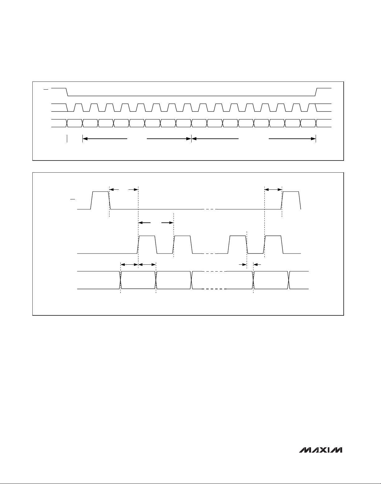
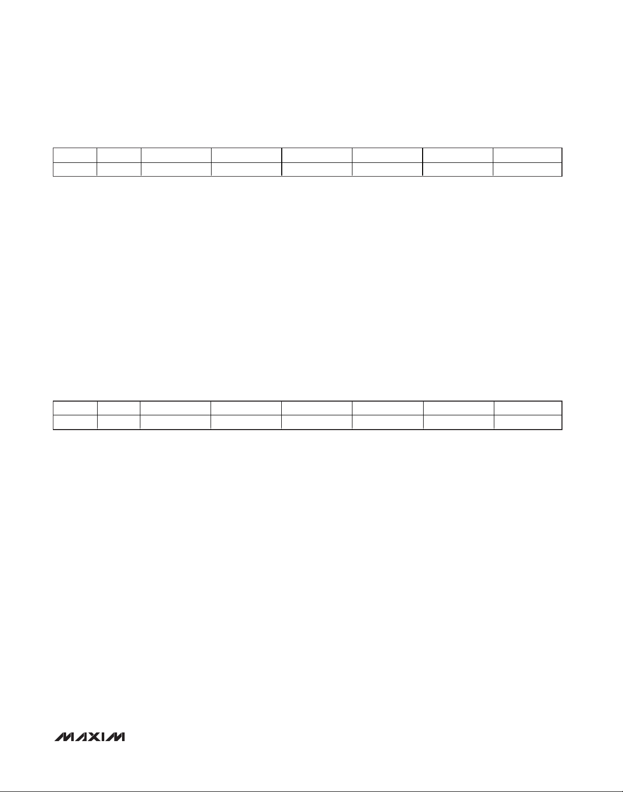
System Timing Requirements
Figures 9 and 10 depict the relationship between the
clock input and output, analog input, sampling event,
and data output. The MAX19515 samples on the rising
edge of the sampling clock. Output data is valid on the
next rising edge of DCLK after a nine-clock internal
latency. For applications where the clock is divided, the
sample clock is the divided internal clock derived from:
[(CLK+ - CLK-)/DIVIDER]
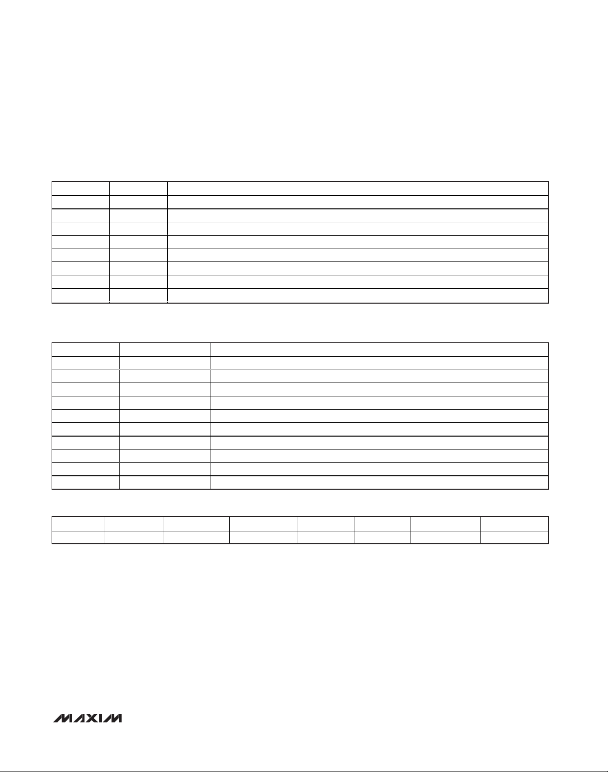
Synchronization
When using the clock divider, the phase of the internal
clock can be different than that of the FPGA, microcontroller, or other MAX19515s in the system. There are
two mechanisms to synchronize the internal clock: slip
synchronization and edge synchronization. Select the
synchronization mode using SYNC_MODE (bit 2) in the
Clock Divide/Data Format/Test Pattern register (06h)
and drive the SYNC input high to synchronize.
Slip Synchronization Mode, SYNC_MODE = 0
(default): On the third rising edge of the input clock
(CLK) after the rising edge of SYNC (provided set-up
and hold times are met), the divided output is forced to
skip a state transition (Figure 11).
Edge Synchronization Mode, SYNC_MODE = 1: On
the third rising edge of the input clock (CLK) after the
rising edge of SYNC (provided set-up and hold times
are met), the divided output is forced to state 0. A divided clock rising edge occurs on the fourth (/2 mode) or
fifth (/4 mode) rising edge of CLK, after a valid rising
edge of SYNC (Figure 12).
DCLK
DATA, DOR
SAMPLE CLOCK
n-9
CHA CHB
n-9 n-8
CHA CHB
n-8
CHB
n-10 n-7
CHA CHB
n-7 n-6
CHA CHB
n-6 n-5
CHA CHB
n-5 n-4
CHA CHB
n-4
MUX OUTPUT MODE
IN_
SAMPLING
INSTANT
SAMPLING
INSTANT
SAMPLING
INSTANT
SAMPLING
INSTANT
SAMPLING
INSTANT
SAMPLING
INSTANT
t
AD
n n+1 n+2 n+4 n+5n+3
t
CH
t
CL
SAMPLE ON RISING EDGE
t
DC
t
DD
t
CHA
t
DCH
t
SETUP
t
HOLD
t
HOLD
t
DCL
t
SETUP
t
CHB
SAMPLE CLOCK IS THE DERIVED CLOCK FROM (CLK+ - CLK-)/CLOCK DIVIDER, IN_ = IN_+ - IN_-.
MUX_CH (BIT 2, OUTPUT FORMAT 01h) DETERMINES THE OUTPUT BUS AND WHICH CHANNEL DATA IS PRESENTED.
t
CLK
Figure 10. Multiplexed Output Mode Timing
Page 26

MAX19515
Dual-Channel, 10-Bit, 65Msps ADC
26 ______________________________________________________________________________________
Figure 11. Slip Synchronization Mode
t
SYNC
2x INPUT CLK
HO
t
SUV
1234
= SET-UP TIME FOR VALID CLOCK EDGE.
t
SUV
= HOLD-OFF TIME FOR INVALID CLOCK EDGE.
t
HO
DIVIDE-BY-2 SLIP SYNCRONIZATION
SLIP
(1) (0) (1) (0) (1) (0) (1) (0) (1) (0)(0)(0)
1x DIVIDED CLK
(STATE)
(1) (0) (1) (0) (1) (0) (1)(1) (0)(1) (0) (1)
t
HO
t
SUV
DIVIDE-BY-4 SLIP SYNCHRONIZATION
SYNC
1234
4x INPUT CLK
1x DIVIDED CLK
(STATE)
5
SLIP
(3)(0) (1) (2) (3) (0) (1) (2) (3) (0) (1) (2) (3)
(0) (1) (2) (3) (0) (1) (2) (3) (0)(1) (2) (3) (0)
(1) (2) (3) (0) (1) (2) (3) (0) (1)(2) (3) (0) (1)
(2) (3) (0) (1) (2) (3) (0) (1)(3) (0) (1) (2) (2)
Page 27
MAX19515
Dual-Channel, 10-Bit, 65Msps ADC
______________________________________________________________________________________ 27
SYNC
Figure 12. Edge Synchronization Mode
2x INPUT CLK
1x DIVIDED CLK
(STATE)
t
HO
t
SUV
= SET-UP TIME FOR VALID CLOCK EDGE.
t
SUV
= HOLD-OFF TIME FOR INVALID CLOCK EDGE.
t
HO
1234
(1) (0) (1) (0) (1) (0) (1) (0) (1) (0) (1)(0)(0)
t
HO
t
SUV
DIVIDE-BY-2 EDGE SYNCRONIZATION
FORCE TO 0
(1) (0) (1) (0) (1) (0) (1) (0) (1)(1) (0)(1) (0)
DIVIDE-BY-4 EDGE SYNCHRONIZATION
SYNC
1234
4x INPUT CLK
1x DIVIDED CLK
(STATE)
5
FORCE TO 0
(0) (1) (2) (3)(0) (1) (2) (3) (0) (1) (2) (3) (0) (1)
(0) (1) (2) (3) (0) (1) (2) (3) (0) (1)(1) (2) (3) (0)
(0) (1) (2) (3) (0) (1) (2) (3) (0) (1)(2) (3) (0) (1)
(0) (1) (2) (3) (0) (1) (2) (3) (0) (1)(3) (0) (1) (2)
Page 28

MAX19515
Dual-Channel, 10-Bit, 65Msps ADC
28 ______________________________________________________________________________________
Digital Outputs
The MAX19515 features a dual CMOS, multiplexable,
reversible data bus. In parallel programming mode,
configure the data outputs (D0_–D9_) for offset binary,
two’s complement, or gray code using the FORMAT
input. Select multiplexed or dual-bus operation using the
OUTSEL input. See the Output Format register (01h) for
details on output formatting using the SPI interface. The
SPI interface offers additional flexibility where D0_–D9_
are reversed, so the LSB appears at D9_ and the MSB
at D0_. OVDD sets the output voltage; set OVDD
between 1.8V and 3.3V. The digital outputs feature programmable output impedance from 50Ω to 300Ω. Set
the output impedance for each bus using the CH_ Data
Output Termination Control registers (04h and 05h).
Programmable Data Timing
The MAX19515 provides programmable data timing control to allow for optimization of timing characteristics to
meet the system timing requirements. The timing adjustment feature also allows for ADC performance improvements by shifting the data output transition away from
the sampling instant. The data timing control signals are
summarized in Table 4. The default settings for timing
adjustment controls are given in Table 5. Many applications will not require adjustment from the default settings.
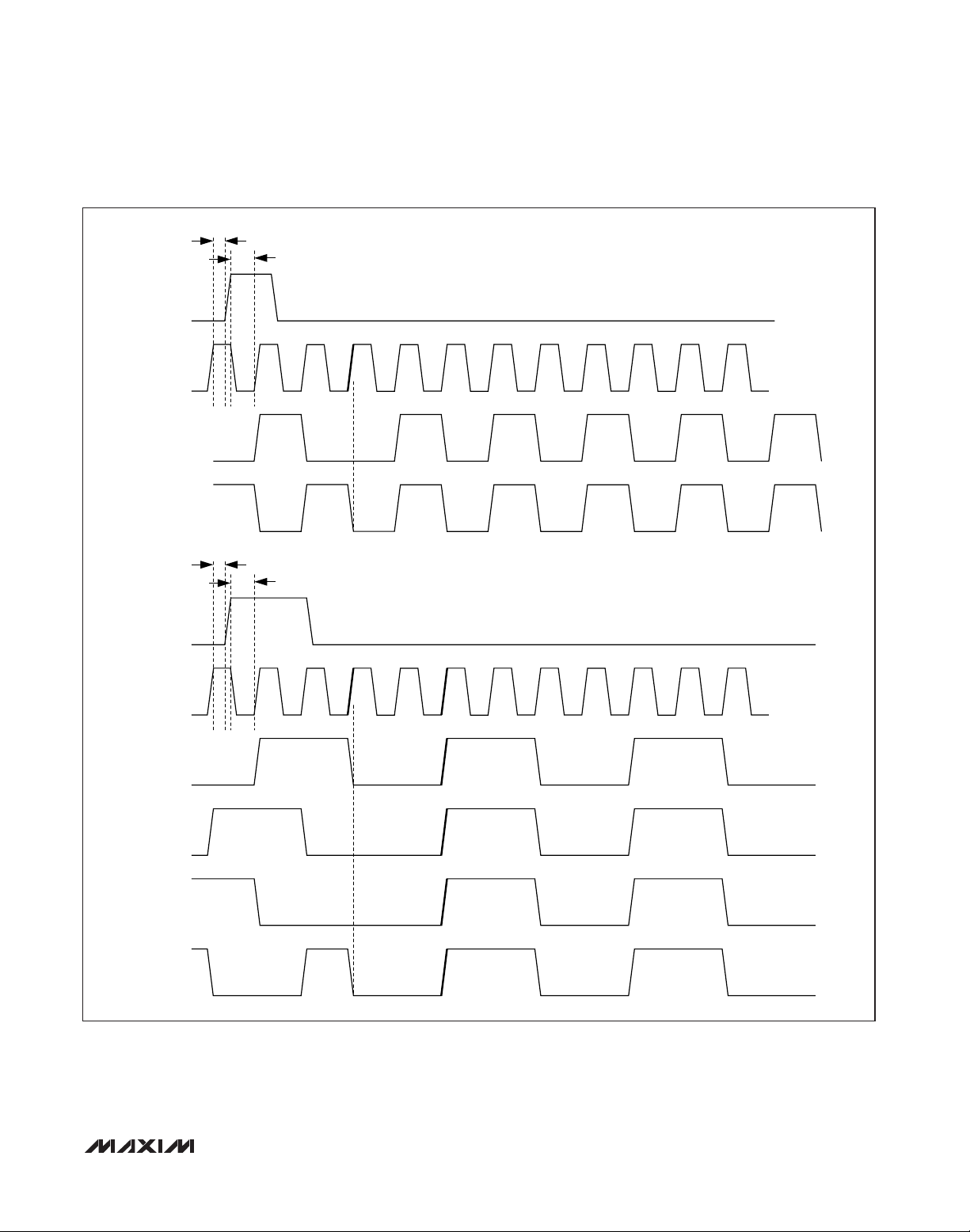
The effects of the data timing adjustment settings are
illustrated in Figures 13 and 14. The x axis is sampling
rate and the y axis is data delay in units of clock period.
The solid lines are the nominal data timing characteristics for the 14 available states of DTIME and
DLY_HALF_T. The heavy line represents the nominal
data timing characteristics for the default settings. Note
that the default timing adjustment setting for the
MAX19515 65Msps ADC results in an additional period
of data latency.
Tables 6 and 7 show the recommended timing control
settings versus sampling rate.
The nominal data timing characteristics versus sampling rate for these recommended timing adjustment
settings are shown in Figures 15 and 16.
When DA_BYPASS = 1, the DCLKTIME delay setting
must be equal to or less than the DTIME delay setting,
as shown in Table 8.
Power Management
The SHDN input (pin 7) toggles between any two powermanagement states. The Power Management register
(00h) defines each power-management state. In default
state, SHDN = 1 shuts down the MAX19515 and SHDN
= 0 returns to full power. Use of the SHDN input is not
required for power management. For either state of
SHDN, complete power-management flexibility is provided, including individual ADC channel power-management control, through the Power Management register
(00h). The available reduced-power modes are shutdown and standby. In standby mode, the reference and
duty-cycle equalizer circuits remain active for rapid
wake-up time. In standby mode, the externally applied
clock signal must remain active for the duty-cycle equalizer to remain locked. Typical wake-up time from standby mode is 15µs. In shutdown mode, all circuits are
turned off except for the reference circuit required for the
integrated self-sensing voltage regulator. If the regulator
is active, there is additional supply current associated
with the regulator circuit when the device is in shutdown.
Typical wake-up time from shutdown mode is 5ms,
which is dominated by the RC time constant on REFIO.
Table 4. Data Timing Controls
Table 5. Data Timing Control Default
Settings
DATA TIMING CONTROL DESCRIPTION
DA_BYPASS
DLY_HALF_T
DTIME<2:0> Allows adjustment of data output delay in T/16 increments, where T is the sample clock period.
DCLKTIME<2:0>
Data aligner bypass. When this control is active (high), data and DCLK delay is reduced by
approximately 3.4ns (relative to DA_BYPASS = 0).
When this control is active, data output is delayed by half clock period (T/2). This control does not
delay data output if MUX mode is active.
Provides adjustment of DCLK delay in T/16 increments, where T is the sample clock period. When
DTIME and DCLKTIME are adjusted to the same setting, the rising edge of DCLK occurs T/8 prior
to data transitions.
DATA TIMING
CONTROL
DA_BYPASS 1 Data aligner disabled
DLY_HALF_T 0 No delay
DTIME<2:0> 000 No delay
DCLKTIME<2:0> 000 No delay
DEFAULT DESCRIPTION
Page 29
MAX19515
Dual-Channel, 10-Bit, 65Msps ADC
______________________________________________________________________________________ 29
Figure 15. Recommended Data Timing (V
OVDD
= 1.8V)
Figure 16. Recommended Data Timing (V
OVDD
= 3.3V)
Table 6. Recommended Timing Adjustments (V
OVDD
= 1.8V)
Figure 13. Default Data Timing (V
OVDD
= 1.8V)
Figure 14. Default Data Timing (V
OVDD
= 3.3V)
FACTORY-DEFAULT NOMINAL DATA
TIMING vs. SAMPLE RATE
2.0
V
= 1.8V
OVDD
DA_BYPASS = 1
1.5
1.0
0.5
DATA DELAY (T FRACTIONAL PERIOD)
0
30 60
SAMPLING RATE (Msps)
FACTORY-DEFAULT NOMINAL DATA
TIMING vs. SAMPLE RATE
2.0
V
= 3.3V
OVDD
DA_BYPASS = 1
1.5
5040
MAX19515 fig13
MAX19515 fig14
+11/16
+9/16
+7/16
+5/16
+3/16
+1/16
-1/16
-3/16
+10/16
+8/16
+6/16
+2/16
0
-2/16
RECOMMENDED DATA TIMING
vs. SAMPLE RATE
2.0
V
= 1.8V
OVDD
DA_BYPASS = 1
1.5
1.0
0.5
DATA DELAY (T FRACTIONAL PERIOD)
0
30 60
5040
SAMPLING RATE (Msps)
RECOMMENDED DATA TIMING
vs. SAMPLE RATE
2.0
V
= 3.3V
OVDD
DA_BYPASS = 1
1.5
MAX19515 fig15
MAX19515 fig16
+11/16
+9/16
+7/16
+5/16
+3/16
+1/16
-1/16
-3/16
+10/16
+8/16
+6/16
+2/16
0
-2/16
1.0
0.5
DATA DELAY (T FRACTIONAL PERIOD)
0
30 60
5040
SAMPLING RATE (Msps)
SAMPLING RATE (Msps) V
+11/16
+9/16
+7/16
+5/16
+3/16
+1/16
-1/16
-3/16
+10/16
+8/16
+6/16
+2/16
0
-2/16
1.0
0.5
DATA DELAY (T FRACTIONAL PERIOD)
0
30 60
5040
SAMPLING RATE (Msps)
= 1.8V
OVDD
FROM TO DA_BYPASS DLY_HALF_T DTIME<2:0> DCLKTIME<2:0>
30 56 1 0 000 000
56 65 1 0 101 101
+11/16
+9/16
+7/16
+5/16
+3/16
+1/16
-1/16
-3/16
+10/16
+8/16
+6/16
+2/16
0
-2/16
Page 30

MAX19515
Dual-Channel, 10-Bit, 65Msps ADC
30 ______________________________________________________________________________________
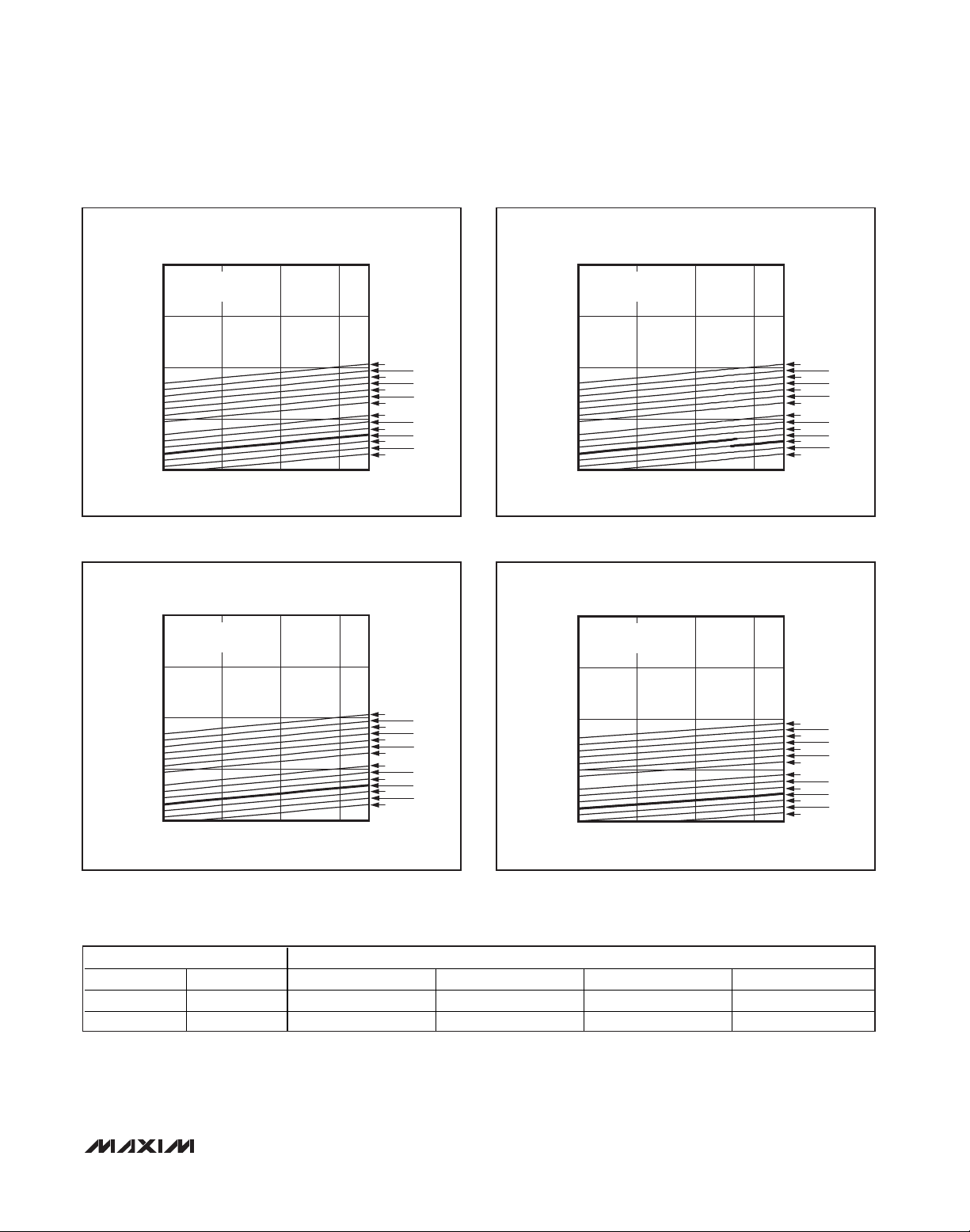
Integrated Voltage Regulator
The MAX19515 includes an integrated self-sensing linear voltage regulator on the analog supply (AVDD). See
Figure 17. When the applied voltage on AVDD is below
2V, the voltage regulator is bypassed, and the core
analog circuitry operates from the externally applied
voltage. If the applied voltage on AVDD is higher than
2V, the regulator bypass switches off, and voltage regulator mode is enabled. When in voltage regulation
mode, the internal-core analog circuitry operates from a
stable 1.8V supply voltage provided by the regulator.
The regulator provides an output voltage of 1.8V over a
2.3V to 3.5V AVDD input-voltage range. Since the
power-supply current is constant over this voltage
range, analog power dissipation is proportional to the
applied voltage.
Power-On and Reset
The user-programmable register default settings and
other factory-programmed settings are stored in nonvolatile memory. Upon device power-up, these values are
loaded into the control registers. This operation occurs
after application of supply voltage to AVDD and application of an input clock signal. The register values are
retained as long as AVDD is applied. While AVDD is
applied, the registers can be reset, which will overwrite all
user-programmed registers with the default values. This
reset operation can be initiated by software command
through the serial-port interface or by hardware control
using the SPEN and SHDN inputs. The reset time is proportional to the ADC clock period and requires 130µs at
65Msps. Table 9 summarizes the reset methods.
Table 7. Recommended Timing Adjustments (V
OVDD
= 3.3V)
Table 8. Allowed Settings of DCLKTIME and DTIME for DA_BYPASS = 1
Table 9. Reset Methods
SAMPLING RATE (Msps) V
FROM TO DA_BYPASS DLY_HALF_T DTIME<2:0> DCLKTIME<2:0>
30 65 1 0 000 000
= 3.3V
OVDD
DTIME<2:0> ALLOWED DCLKTIME<2:0> SETTINGS
111 (-3T/16) 111 (-3T/16)
110 (-2T/16) 110 (-2T/16); 111 (-3T/16)
101 (-1T/16) 101 (-1T/16); 110 (-2T/16); 111 (-3T/16)
000 (nominal) 000 (nominal); 101 (-1T/16); 110 (-2T/16); 111 (-3T/16)
001 (+1T/16) 001 (+1T/16); 000 (nominal); 101 (-1T/16); 110 (-2T/16); 111 (-3T/16)
010 (+2T/16) 010 (+2T/16); 001 (+1T/16); 000 (nominal); 101 (-1T/16); 110 (-2T/16); 111 (-3T/16)
011 (+3T/16) 011 (+3T/16); 010 (+2T/16); 001 (+1T/16); 000 (nominal); 101 (-1T/16); 110 (-2T/16); 111 (-3T/16)
RESET MODE DESCRIPTION
Power-On Reset
Software Reset Write data 5Ah to address 0Ah to initiate register reset.
Hardware Reset A register reset is initiated by the falling edge on the SHDN pin when SPEN is high.
Upon power-up (AVDD supply voltage and clock signal applied), the POR (power-on-reset) circuit initiates a
register reset.
Page 31
MAX19515
Dual-Channel, 10-Bit, 65Msps ADC
______________________________________________________________________________________ 31
Applications Information
Analog Inputs
Transformer-Coupled Differential Analog Input
The MAX19515 provides better SFDR and THD with
fully differential input signals than a single-ended input
drive. In differential input mode, even-order harmonics
are lower as both inputs are balanced, and each of the
ADC inputs only require half the signal swing compared
to single-ended input mode.
An RF transformer (Figure 18) provides an excellent
solution for converting a single-ended signal to a fully
differential signal. Connecting the center tap of the
transformer to CM_ provides a common-mode voltage.
The transformer shown has an impedance ratio of 1:1.4.
Alternatively, a different step-up transformer can be
selected to reduce the drive requirements. A reduced
signal swing from the input driver can also improve the
overall distortion. The configuration of Figure 18 is good
for frequencies up to Nyquist (f
CLK
/2).
Figure 17. Integrated Voltage Regulator
Figure 19. Transformer-Coupled Input Drive for Input Frequencies Beyond Nyquist
Figure 18. Transformer-Coupled Input Drive for Input
Frequencies Up to Nyquist
(PINS 1, 12, 13, 48)
AVDD
REFERENCE
GND
IN_+
0.1µF
V
IN
1
5
N.C. N.C.
3
MINI-CIRCUITS
ADT1-1WT
T1
36.5Ω
0.5%
6
2
4
36.5Ω
0.5%
0.1µF
MAX19515
CM_
IN_-
REGULATOR
IN
2.3V TO 3.5V
ENABLE
OUT
1.8V
INTERNAL
ANALOG
CIRCUITS
V
IN
0.1µF
N.C.
MINI-CIRCUITS
1
T1
5
3
ADT1-1WT
6
2
N.C.
4
75Ω
0.5%
75Ω
0.5%
1
5
N.C.
3
MINI-CIRCUITS
ADT1-1WT
6
T2
2
N.C.
4
110Ω
0.5%
0.1µF
110Ω
0.5%
IN_+
MAX19515
CM_
IN_-
Page 32
MAX19515
Dual-Channel, 10-Bit, 65Msps ADC
32 ______________________________________________________________________________________
The circuit of Figure 19 also converts a single-ended
input signal to a fully differential signal. Figure 19 utilizes an additional transformer to improve the commonmode rejection allowing high-frequency signals beyond
the Nyquist frequency. A set of 75Ω and 110Ω termina-
tion resistors provide an equivalent 50Ω termination to
the signal source. The second set of termination resistors connect to CM_ providing the correct input common-mode voltage.
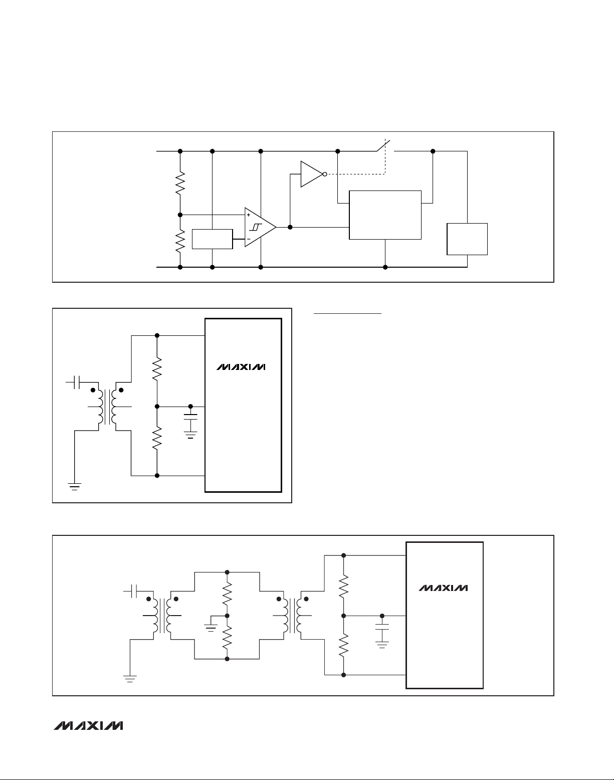
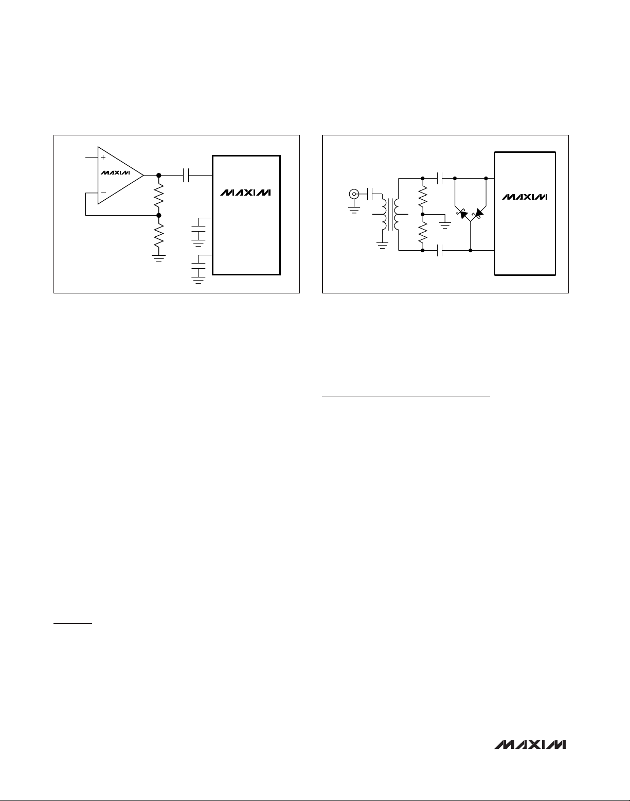
Single-Ended AC-Coupled Input Signal
Figure 20 shows a single-ended, AC-coupled input
application. The MAX4108 provides high speed, high
bandwidth, low noise, and low distortion to maintain the
input signal integrity. Bias voltage is applied to the
inputs through internal 2kΩ resistors. See Common
Mode register 08h for further details.
DC-Coupled Input
The MAX19515’s wide common-mode voltage range
(0.4V to 1.4V) allows DC-coupled signals. Ensure that the
common-mode voltage remains between 0.4V and 1.4V.
Clock Input
Figure 21 shows a single-ended-to-differential clock
input converting circuit.
Grounding, Bypassing, and
Board-Layout Considerations
The MAX19515 requires high-speed board-layout
design techniques. Locate all bypass capacitors as
close as possible to the device, preferably on the same
side as the ADC, using surface-mount devices for minimum inductance. Bypass AVDD, OVDD, REFIO, CMA,
and CMB with 0.1µF ceramic capacitors to GND.
Multilayer boards with ground and power planes pro-
duce the highest level of signal integrity. Route highspeed digital signal traces away from the sensitive analog traces of either channel. Make sure to isolate the
analog input lines to each respective converter to minimize channel-to-channel crosstalk. Keep all signal lines
short and free of 90° turns.
Definitions
Integral Nonlinearity (INL)
INL is the deviation of the measured transfer function
from a best-fit straight line. Worst-case deviation is
defined as INL.
Differential Nonlinearity (DNL)
DNL is the difference between the measured transfer
function step width and the ideal value of 1 LSB. A DNL
error specification of less than 1 LSB guarantees no
missing codes and a monotonic transfer function. DNL
deviations are measured at each step of the transfer
function and the worst-case deviation is defined as DNL.
Offset Error
Offset error is a parameter that indicates how well the
actual transfer function matches the ideal transfer function at midscale. Ideally, the midscale transition occurs
at 0.5 LSB above midscale. The offset error is the
amount of deviation between the measured midscale
transition point and the ideal midscale transition point.
Gain Error
Gain error is a figure of merit that indicates how well the
slope of the measured transfer function matches the
slope of the ideal transfer function based on the specified full-scale input-voltage range. The gain error is
defined as the relative error of the measured transfer
function and is expressed as a percentage.
Figure 20. Single-Ended, AC-Coupled Input Drive
Figure 21. Single-Ended-to-Differential Clock Input
V
IN
MAX4108
100Ω
100Ω
0.1µF
0.1µF
0.1µF
IN_+
MAX19515
CM_
IN_-
0.1µF
CLKIN
49.9Ω
49.9Ω
0.01µF
CLK+
MAX19515
0.01µF
CLK-
Page 33

MAX19515
Dual-Channel, 10-Bit, 65Msps ADC
______________________________________________________________________________________ 33
Small-Signal Noise Floor (SSNF)
SSNF is the integrated noise and distortion power in the
Nyquist band for small-signal inputs. The DC offset is
excluded from this noise calculation. For this converter, a
small signal is defined as a single tone with an amplitude
less than -35dBFS. This parameter captures the thermal
and quantization noise characteristics of the converter
and can be used to help calculate the overall noise figure
of a receive channel. Refer to www.maxim-ic.com for
application notes on Thermal + Quantization Noise Floor.
Signal-to-Noise Ratio (SNR)
For a waveform perfectly reconstructed from digital
samples, the theoretical maximum SNR is the ratio of
the full-scale analog input (RMS value) to the RMS
quantization error (residual error). The ideal, theoretical
minimum analog-to-digital noise is caused by quantization error only and results directly from the ADC’s resolution (N bits):
SNR
[max]
= 6.02 x N + 1.76
In reality, there are other noise sources besides quantization noise (e.g., thermal noise, reference noise, clock
jitter, etc.). SNR is computed by taking the ratio of the
RMS signal to the RMS noise. RMS noise includes all
spectral components to the Nyquist frequency excluding the fundamental, the first six harmonics (HD2–HD7),
and the DC offset.
Signal-to-Noise and Distortion (SINAD)
SINAD is computed by taking the ratio of the RMS signal to the RMS noise plus the RMS distortion. RMS
noise includes all spectral components to the Nyquist
frequency excluding the fundamental, the first six harmonics (HD2–HD7), and the DC offset. RMS distortion
includes the first six harmonics (HD2–HD7).
Single-Tone Spurious-Free Dynamic Range
(SFDR1 and SFDR2)
SFDR is the ratio expressed in decibels of the RMS
amplitude of the fundamental (maximum signal component) to the RMS amplitude of the next largest spurious
component, excluding DC offset. SFDR1 reflects the
spurious performance based on worst 2nd-order or
3rd-order harmonic distortion. SFDR2 is defined by the
worst spurious component excluding 2nd- and 3rdorder harmonics and DC offset.
Total Harmonic Distortion (THD)
THD is the ratio of the RMS of the first six harmonics of
the input signal to the fundamental itself. This is
expressed as:
where V1is the fundamental amplitude and V2–V7are
the amplitudes of the 2nd-order through 7th-order harmonics (HD2–HD7).
Third-Order Intermodulation (IM3)
IM3 is the total power of the third-order intermodulation
products to the Nyquist frequency relative to the total
input power of the two input tones f
IN1
and f
IN2
. The
individual input tone levels are at -7dBFS. The thirdorder intermodulation products are: 2 x f
IN1
- f
IN2
, 2 x
f
IN2
- f
IN1
, 2 x f
IN1
+ f
IN2
, 2 x f
IN2
+ f
IN1
.
Aperture Delay
The input signal is sampled on the rising edge of the
sampling clock. There is a small delay between the rising edge of the sampling clock and the actual sampling
instant, which is defined as aperture delay (t
AD
).
Aperture Jitter
Aperture jitter (tAJ) is defined as the sample-to-sample
time variation in the aperture delay.
Overdrive Recovery Time
Overdrive recovery time is the time required for the
ADC to recover from an input transient that exceeds the
full-scale limits. The specified overdrive recovery time is
measured with an input transient that exceeds the fullscale limits by ±10%.
Chip Information
PROCESS: CMOS
SNR
log =×
20
⎛
SIGNAL
⎜
NOISE
⎝
RMS
RMS
⎞
⎟
⎠
THD
log
=×
20
⎛
232
VVVVVV
+++++
2
⎜
⎜
⎝
2
2
4
V
1
2
5
6
⎞
2
7
⎟
⎟
⎠
SINAD
log
=×
20
⎛
⎜
⎜
NOISE DISTORTION
⎝
SIGNAL
RMS
22
+
RMS RMS
⎞
⎟
⎟
⎠
Page 34

TOP VIEW
MAX19515
13
14
15
16
17
18
19
20
21
22
23
24
AVDD
SYNC
CLK+
CLK-
GND
GND
DORB
DCLKB
D0B
D1B
D2B
D3B
48
47
46
45
44
43
42
41
40
39
38
37
1
2
345678910
11
12
AVDD
CS/OUTSEL
SCLK/DIV
SDIN/FORMAT
DCLKA
DORA
D9A
D8A
D7A
D6A
D5A
D4A
AVDD
CMB
INB-
INB+
I.C.
SHDN
REFIO
SPEN
INA-
INA+
CMA
AVDD
36
35
34 33 32 31 30 29 28 27
26
25
OVDD
D4B
D5B
D6B
D7B
D8B
D9B
D0A
D1A
D2A
D3A
OVDD
+
*EP
*EXPOSED PAD
Pin Configuration
MAX19515
Dual-Channel, 10-Bit, 65Msps ADC
34 ______________________________________________________________________________________
Package Information
For the latest package outline information and land patterns (footprints), go to www.maxim-ic.com/packages. Note that a “+”, “#”, or
“-” in the package code indicates RoHS status only. Package drawings may show a different suffix character, but the drawing pertains to the package regardless of RoHS status.
PACKAGE TYPE PACKAGE CODE OUTLINE NO.
LAND
PATTERN NO.
48 TQFN-EP T4877+4
21-0144
90-0130
Page 35
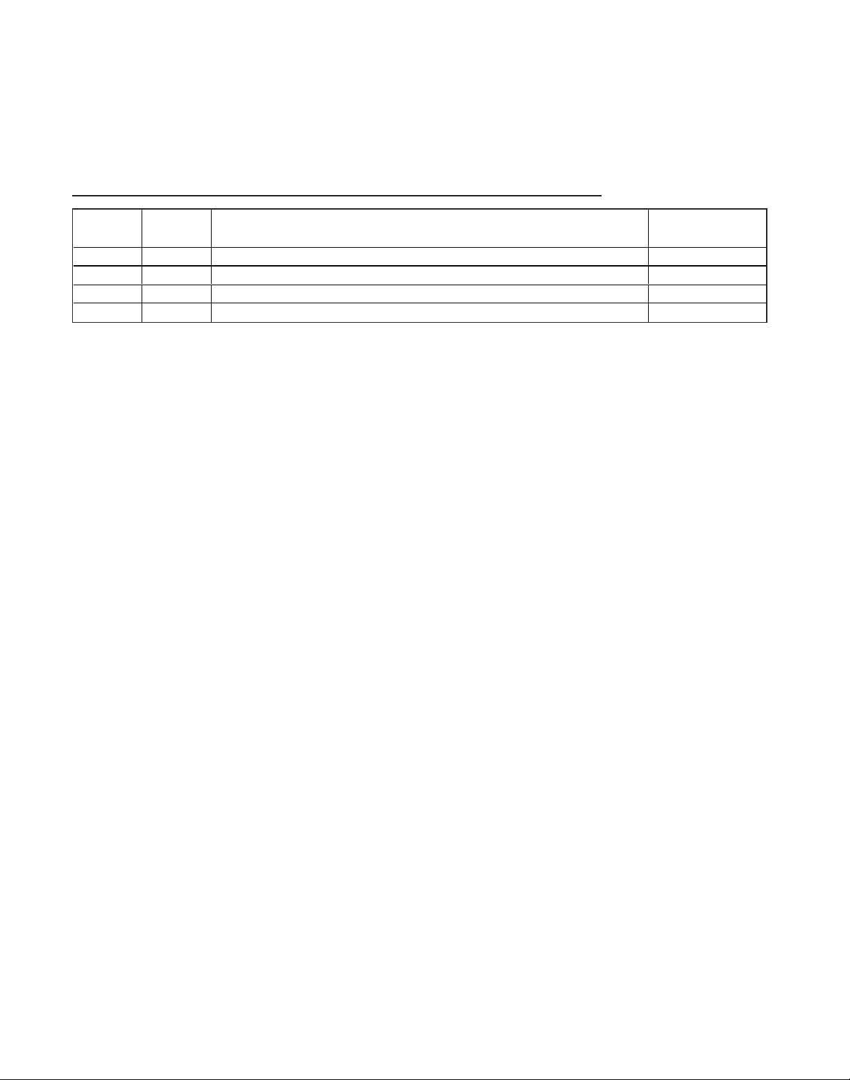
MAX19515
Dual-Channel, 10-Bit, 65Msps ADC
Maxim cannot assume responsibility for use of any circuitry other than circuitry entirely embodied in a Maxim product. No circuit patent licenses are
implied. Maxim reserves the right to change the circuitry and specifications without notice at any time.
Maxim Integrated Products, 120 San Gabriel Drive, Sunnyvale, CA 94086 408-737-7600 ____________________
35
© 2011 Maxim Integrated Products Maxim is a registered trademark of Maxim Integrated Products, Inc.
Revision History
REVISION
NUMBER
0 7/08 Initial release —
1 10/08 Corrected error in vertical scale for TOC32 11
2 9/10 Updated timing characteristics due to CMOS output driver changes 5, 6, 28, 29, 30
3 1/11 Added automotive qualified part to Ordering Information 1
REVISION
DATE
DESCRIPTION
PAGES
CHANGED
 Loading...