

Page 1
General Description
The MAX1945R/MAX1945S high-efficiency pulse-width
modulation (PWM) switching regulators deliver up to 6A
of output current. The devices operate from an input
supply range of 2.6V to 5.5V and provide selectable
output voltages of 1.8V, 2.5V, and adjustable output
voltages from 0.8V to 85% of the supply voltage. With
VCCat 3.3V/5V, the input voltage can be as low as
2.25V. The MAX1945R/MAX1945S are ideal for onboard post-regulation applications. Total output voltage
error is less than ±1% over load, line, and temperature.
The MAX1945R/MAX1945S operate at a selectable
fixed frequency (500kHz or 1MHz) or can be synchronized to an external clock (400kHz to 1.2MHz). The
high operating frequency minimizes the size of external
components. The high bandwidth of the internal error
amplifier provides excellent transient response. The
MAX1945R/MAX1945S have internal dual N-channel
MOSFETs to lower heat dissipation at heavy loads. Two
MAX1945R/MAX1945Ss can operate 180 degrees outof-phase of each other to minimize input capacitance.
The devices provide output voltage margining for
board-level testing. The MAX1945R provides a ±4%
voltage margining. The MAX1945S provides a ±9%
voltage margining.
The MAX1945R/MAX1945S are available in 28-pin
TSSOP-EP packages and are specified over the -40°C
to +85°C industrial temperature range. An evaluation kit
is available to speed designs.
Applications
Low-Voltage, High-Density Distributed Power
Supplies
ASIC, CPU, and DSP Core Voltages
RAM Power Supply
Base Station, Telecom, and Networking
Equipment Power Supplies
Server and Notebook Power Supplies
Features
♦ 6A PWM Step-Down Regulator with 95%
Efficiency
♦ 1MHz/500kHz Switching for Small External
Components
♦ 0.76in
2
Complete 6A Regulator Footprint
♦ External Components’ Height <3mm
♦ ±1% Output Accuracy over Load, Line, and
Temperature
♦ Operate from 2.6V to 5.5V Supply
♦ Operate from 2.5V Input with V
CC
at 3.3V/5V
♦ Preset Output Voltage of 1.8V or 2.5V
♦ Adjustable Output from 0.8V to 85% of Input
♦ Voltage Margining: ±4% (MAX1945R) or ±9%
(MAX1945S)
♦ Synchronize to External Clock
♦ SYNCOUT Provides 180-Degree Out-of-Phase
Clock Output
♦ All-Ceramic or Electrolytic Capacitor Designs
MAX1945R/MAX1945S
1MHz, 1% Accurate, 6A Internal Switch
Step-Down Regulators
________________________________________________________________ Maxim Integrated Products 1
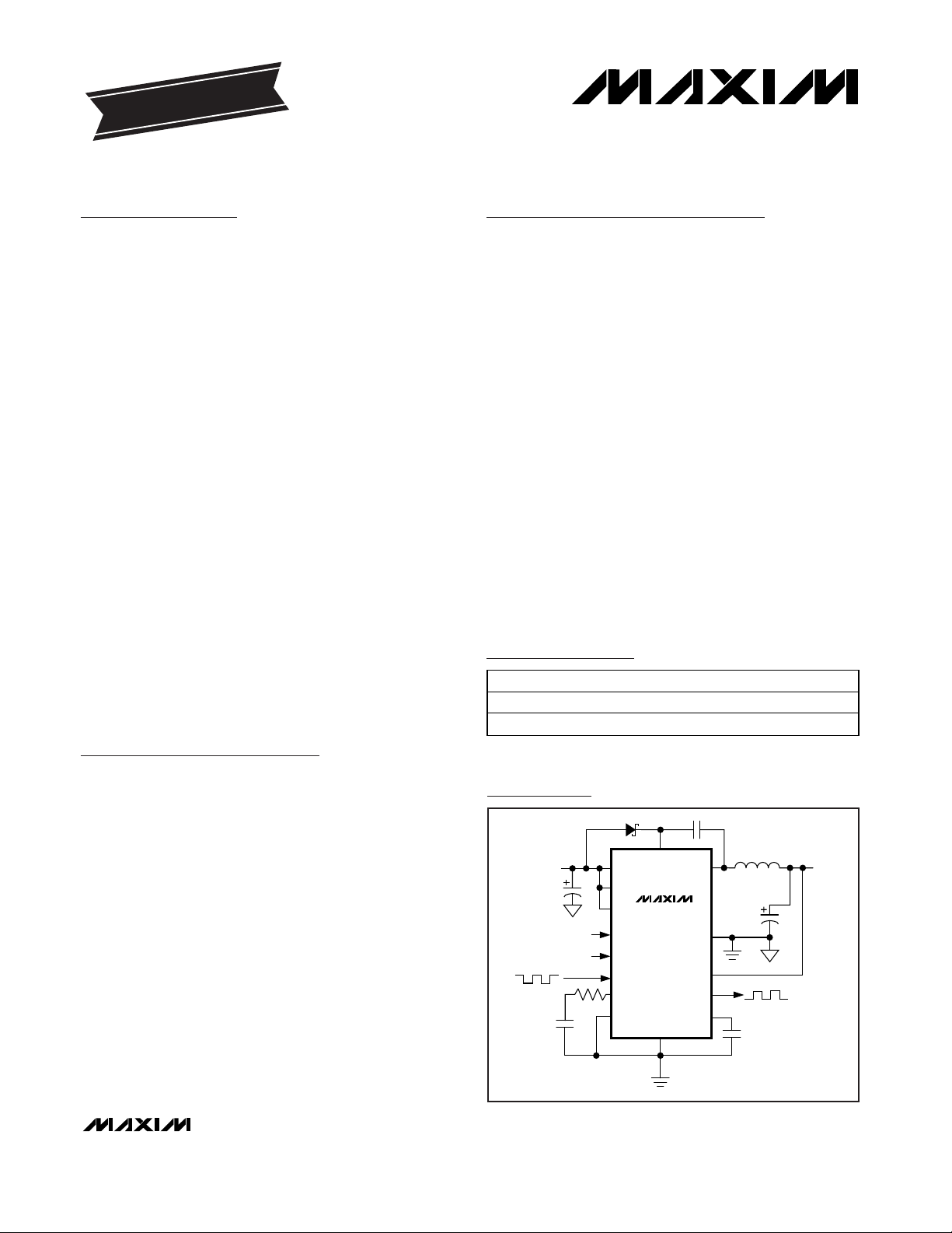
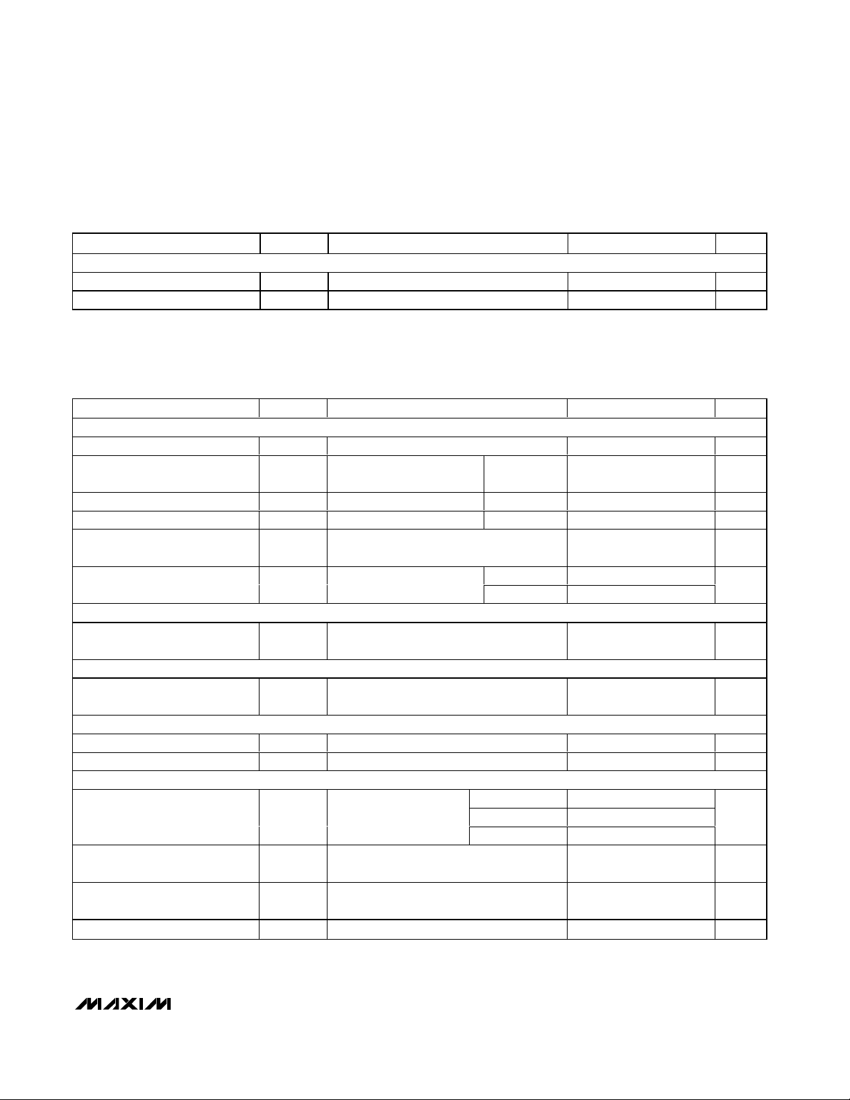
Ordering Information
IN
FB
REF
COMP
LX
BST
GND
V
CC
PGND
INPUT
2.6V TO 5.5V
FBSEL
CTL1
CTL2
SYNC
SYNCOUT
OUTPUT
0.8V TO
0.85 x V
IN
,
6A
VOLTAGE
MARGINING
ON/OFF
SYNCHRONIZATION
CLOCK
V
DD
MAX1945R
MAX1945S
180° OUT-OF-PHASE
Typical Operating Circuit
19-2640; Rev 1; 7/04
For pricing, delivery, and ordering information, please contact Maxim/Dallas Direct! at
1-888-629-4642, or visit Maxim’s website at www.maxim-ic.com.
*EP = Exposed pad.
Pin Configuration appears at end of data sheet.
EVALUATION KIT
AVAILABLE
PART TEMP RANGE PIN-PACKAGE
MAX1945REUI -40°C to +85°C 28 TSSOP-EP*
MAX1945SEUI -40°C to +85°C 28 TSSOP-EP*
Page 2
MAX1945R/MAX1945S
1MHz, 1% Accurate, 6A Internal Switch
Step-Down Regulators
2 _______________________________________________________________________________________
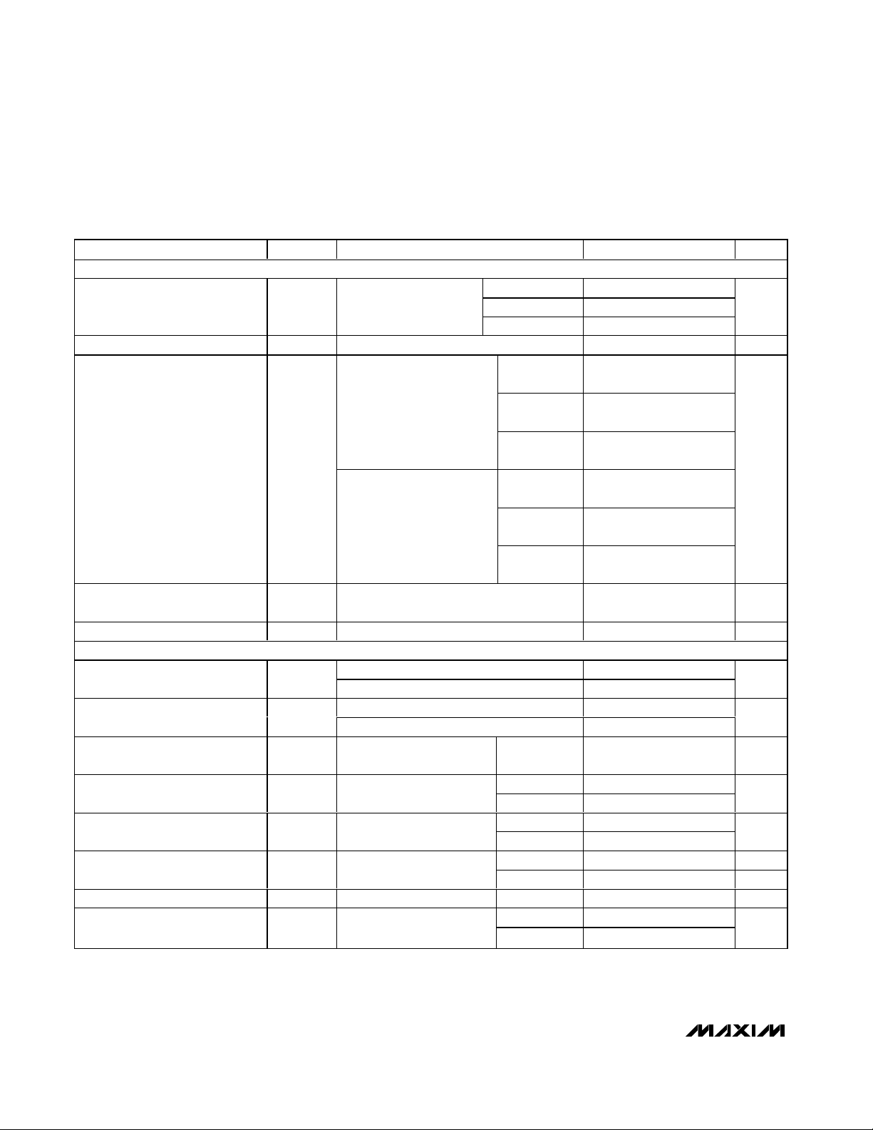
ABSOLUTE MAXIMUM RATINGS
ELECTRICAL CHARACTERISTICS
(VIN= VCC= V
CTL1
= V
CTL2
= VDD= 3.3V, SYNC = GND, FBSEL = High-Z, VFB= 0.7V, C
REF
= 0.22µF, TA= 0°C to +85°C, unless
otherwise noted. Typical values are at +25°C.)
Stresses beyond those listed under “Absolute Maximum Ratings” may cause permanent damage to the device. These are stress ratings only, and functional
operation of the device at these or any other conditions beyond those indicated in the operational sections of the specifications is not implied. Exposure to
absolute maximum rating conditions for extended periods may affect device reliability.
CTL1, CTL2, IN, SYNC, VCC, VDDto GND...............-0.3V to +6V
SYNCOUT, COMP, FB, FBSEL,
REF to GND............................................-0.3V to (V
CC
+ 0.3V)
LX Current (Note 1) .....................................................-9A to +9A
BST to LX..................................................................-0.3V to +6V
PGND to GND .......................................................-0.3V to +0.3V
Continuous Power Dissipation (T
A
= +85°C)
(derate 23.8mW/°C above +70°C).............................1191mW
Operating Temperature Range ...........................-40°C to +85°C
Storage Temperature Range .............................-65°C to +150°C
Lead Temperature (soldering, 10s) .................................+300°C
PARAMETER
SYMBOL
CONDITIONS
MIN
TYP
MAX
UNITS
IN/V
CC
Input Voltage V
IN
2.6 5.5 V
V
IN
= 3.3V 12 20
IN Supply Current I
IN
SYNC = VCC (1MHz),
no load
V
IN
= 5.5V 48
mA
V
CC
= 3.3V 2 3
VCC Supply Current I
CC
SYNC = VCC (1MHz)
V
CC
= 5.5V 3
mA
V
DD
= 3.3V 5 8
VDD Supply Current I
DD
SYNC = VCC (1MHz)
V
DD
= 5.5V 10
mA
Total Shutdown Current from IN,
V
CC
, and V
DD
I
TOTAL
V
IN
= VCC = V
DD
= V
BST
- V
LX
= 5.5V,
CTL1 = CTL2 = GND
500 µA
VCC rising
VCC Undervoltage Lockout
Threshold
V
UVLO
When LX starts/stops
switching
V
CC
falling
V
V
DD
V
DD
Shutdown Supply Current
V
IN
= V
DD
= V
BST
= 5.5V, V
LX
= 5.5V or 0,
CTL1 = CTL2 = GND
10 µA
BST
BST Shutdown Supply Current I
BST
V
IN
= V
DD
= V
BST
= 5.5V, V
LX
= 5.5V or 0,
CTL1 = CTL2 = GND
10 µA
REF
REF Voltage V
REF
I
REF
= 0, V
IN
= 2.6V to 5.5V
V
REF Shutdown Resistance From REF to GND, CTL1 = CTL2 = GND 10 100 Ω
COMP
30 55 85
FBSEL = GND
COMP Transconductance
From FB to COMP,
V
COMP
= 1.25V
FBSEL = V
CC
9.6
µS
COMP Clamp Voltage Low
V
LOW_
CLAMP
V
IN
= 2.6V to 5.5V, V
FB
= 0.9V 0.5 0.8 1.1 V
COMP Clamp Voltage High
V
HIGH_
CLAMP
V
IN
= 2.6V to 5.5V, V
FB
= 0.7V
V
COMP Shutdown Resistance
10 100 Ω
Note 1: LX has internal clamp diodes to PGND and IN. Applications that forward bias these diodes should take care not to exceed
the IC’s package power dissipation limits.
From COMP to GND, CTL1 = CTL2 = GND
2.20 2.35
1.97 2.00 2.04
FBSEL = High-Z
13.3 24.4 37.8
1.90 2.15 2.40
2.40 2.55
17.6 27.2
Page 3
MAX1945R/MAX1945S
1MHz, 1% Accurate, 6A Internal Switch
Step-Down Regulators
_______________________________________________________________________________________ 3
ELECTRICAL CHARACTERISTICS (continued)
(VIN= VCC= V
CTL1
= V
CTL2
= VDD= 3.3V, SYNC = GND, FBSEL = High-Z, VFB= 0.7V, C
REF
= 0.22µF, TA= 0°C to +85°C, unless
otherwise noted. Typical values are at +25°C.)
PARAMETER
CONDITIONS
UNITS
FB
FBSEL = V
CC
FB Regulation Voltage
(Error Amp Only)
V
FB
V
COMP
= 1V to 2V,
V
IN
= 2.6V to 5.5V
V
Maximum Output Current
V
IN
= 3.3V, V
OUT
= 1.8V, L = 1µH 6 A
-1 +1
CTL2 = V
CC
35
MAX1945R,
V
COMP
= 1V to 2V,
V
IN
= 2.6V to 5.5V
-5 -3
-1 +1
CTL2 = V
CC
810
FB Voltage Margining Output
(Error Amp Only)
MAX1945S,
V
COMP
= 1V to 2V,
V
IN
= 2.6V to 5.5V
-10 -8
%
FB Input Resistance
FB to GND, FBSEL = GND, or V
FB
= 1.8V,
or FBSEL = V
CC
, or V
FB
= 2.5V
25 50 100 kΩ
FB Input Bias Current FBSEL = High-Z, V
FB
= 0.7V
µA
LX
V
IN
= V
BST
- V
LX
= 3.3V 26 43
LX On-Resistance High
R
ON_HIGH_
LX V
IN
= V
BST
- V
LX
= 2.6V 30 50
mΩ
V
IN
= 3.3V 26 43
LX On-Resistance Low
R
ON_LOW_
LX V
IN
= 2.6V 30 50
mΩ
LX Current-Sense
Transresistance
From LX to COMP 43 54 65 mΩ
High side 8.0
LX Current-Limit Threshold
Duty cycle =100%,
V
IN
= 2.6V/3.3V/5.5V
Low side -6 -4 -2
A
V
LX
= 5.5V 100
LX Leakage Current
V
IN
= 5.5V,
CTL1 = CTL2 = GND
LX = GND
µA
0.8 1.0
1.2
MHz
LX Switching Frequency f
SW
V
IN
= 2.6V/3.3V
600 kHz
LX Minimum Off-Time t
OFF
V
IN
= 2.6V/3.3V
180 ns
90
LX Maximum Duty Cycle VIN = 2.6V/3.3V
80
%
SYMBOL
I
FB_OUT
V
MARGIN_
MIN TYP MAX
FBSEL = GND 1.782 1.800 1.818
2.475 2.500 2.525
FBSEL = High-Z 0.792 0.800 0.808
CTL1 = VCC,
CTL2 = V
CC
CTL1 = GND,
CTL1 = VCC,
CTL2 = GND
CTL1 = VCC,
CTL2 = V
CC
CTL1 = GND,
CTL1 = VCC,
CTL2 = GND
0.01 0.10
I
LEAK_LX
-100
SYNC = V
CC
SYNC = GND 400 500
SYNC = GND
SYNC = V
CC
10.4 12.8
155
Page 4
MAX1945R/MAX1945S
1MHz, 1% Accurate, 6A Internal Switch
Step-Down Regulators
4 _______________________________________________________________________________________
ELECTRICAL CHARACTERISTICS (continued)
(VIN= VCC= V
CTL1
= V
CTL2
= VDD= 3.3V, SYNC = GND, FBSEL = High-Z, VFB= 0.7V, C
REF
= 0.22µF, TA= 0°C to +85°C, unless
otherwise noted. Typical values are at +25°C.)
PARAMETER
CONDITIONS
UNITS
8.8
LX Minimum Duty Cycle VIN = 2.6V/3.3V
%
RMS LX Output Current 6A
FBSEL
FBSEL Input Threshold 1.8V
Where 1.8V feedback
switches in and out,
V
CC
= 2.6V/3.3V/5.5V
V
V
CC -
V
CC
-
FBSEL Input Threshold 2.5V
Where 2.5V feedback
switches in and out,
V
CC
= 2.6V/3.3V/5.5V
V
CC
-
V
CC
-
V
FBSEL Input Current Low
I
LOW_
FBSEL
FBSEL = GND -50 -20 µA
FBSEL Input Current High
I
HIGH_
FBSEL
FBSEL = V
CC
20 50 µA
CTL1 /CTL2
0.4
CTL1/CTL2 Input Threshold
V
IN
= 2.6V to 5.5V
1.0 1.6
V
-1 +1
CTL1/CTL2 Input Current
V
CTL1
or V
CTL2
= 0 or 5.5V, V
IN
= 5.5V
-1 +1
µA
Soft-Start Period Time required for output to ramp up 2.9 3.7 4.5 ms
+4%
Time from Nominal to Margin
High
+9%
µs
-4%
Time from Nominal to Margin Low
-9%
µs
SYNC
SYNC Capture Range V
IN
= 2.6V to 5.5V 0.4 1.2
MHz
SYNC Pulse Width
t
LO, tHI
V
IN
= 2.6V to 5.5V
ns
SYNC Input Threshold
V
IN
= 2.6V to 5.5V
1.0 1.6
V
SYNC Input Current I
IL, IIH
V
SYNC
= 0 or 5.5V, V
IN
= 5.5V -1 +1 µA
SYNCOUT
SYNCOUT Frequency Range
V
CC
= 2.6V to 5.5V 0.4 1.2
MHz
V
OH_SYNC
OUT
V
CC
-
0.4
V
CC
-
SYNCOUT Output Voltage
V
OL_SYNC
OUT
I
SYNCOUT
= ±1mA, V
CC
= 2.6V to 5.5V
V
SYMBOL
MIN TYP MAX
SYNC = GND
SYNC = V
CC
FBSEL rising 0.16 0.22
FBSEL falling 0.08 0.14
10.5
17.6
FBSEL rising
FBSEL falling
0.22
0.14
0.16
0.08
V
IL_CTL_
V
IH_CTL_
I
IL_CTL_
I
IH_CTL_
t
HIGH_4%
t
HIGH_9%
t
t
V
V
LOW_4%
LOW_9%
IL_SYNC
IH_SYNC
250
0.40 0.95
f
SYNCOUT
0.95
160
360
450
1000
0.05
0.05 0.40
Page 5
MAX1945R/MAX1945S
1MHz, 1% Accurate, 6A Internal Switch
Step-Down Regulators
_______________________________________________________________________________________ 5
ELECTRICAL CHARACTERISTICS (continued)
(VIN= VCC= V
CTL1
= V
CTL2
= VDD= 3.3V, SYNC = GND, FBSEL = High-Z, VFB= 0.7V, C
REF
= 0.22µF, TA= 0°C to +85°C, unless
otherwise noted. Typical values are at +25°C.)
PARAMETER
CONDITIONS
UNITS
THERMAL SHUTDOWN
Thermal-Shutdown Hysteresis 20 °C
Thermal-Shutdown Threshold When LX stops switching
°C
ELECTRICAL CHARACTERISTICS
(VIN= VCC= V
CTL1
= V
CTL2
= VDD= 3.3V, SYNC = GND, FBSEL = High-Z, VFB= 0.7V, C
REF
= 0.22µF, TA= -40°C to +85°C, unless
otherwise noted.) (Note 2)
PARAMETER
SYMBOL
CONDITIONS
MIN
TYP
MAX
UNITS
IN/V
CC
Input Voltage V
IN
2.6 5.5 V
IN Supply Current I
IN
SYNC = VCC (1MHz),
no load
V
IN
= 3.3V 20 mA
VCC Supply Current I
CC
SYNC = VCC (1MHz) V
CC
= 3.3V 4 mA
VDD Supply Current I
DD
SYNC = VCC (1MHz) V
DD
= 3.3V 8 mA
Total Shutdown Current from IN,
V
CC
, and V
DD
I
TOTAL
V
IN
= VCC = V
DD
= V
BST
- V
LX
= 5.5V,
CTL1 = CTL2 = GND
500 µA
VCC rising
VCC Undervoltage Lockout
Threshold
V
UVLO
When LX starts/stops
switching
V
CC
falling
V
V
DD
V
DD
Shutdown Supply Current I
VDD
V
IN
= V
DD
= V
BST
= 5.5V, V
LX
= 5.5V or 0,
CTL1 = CTL2 = GND
10 µA
BST
BST Shutdown Supply Current I
BST
V
IN
= V
DD
= V
BST
= 5.5V, V
LX
= 5.5V or 0,
CTL1 = CTL2 = GND
10 µA
REF
REF Voltage V
REF
I
REF
= 0, V
IN
= 2.6V to 5.5V
V
REF Shutdown Resistance From REF to GND, CTL1 = CTL2 = GND 100 Ω
COMP
30 85
FBSEL = GND
COMP Transconductance
From FB to COMP,
V
COMP
= 1.25V
FBSEL = V
CC
9.6
µS
COMP Clamp Voltage Low
V
LOW_
CLAMP
V
IN
= 2.6V to 5.5V, V
FB
= 0.9V 0.5 1.1 V
COMP Clamp Voltage High
V
HIGH_
CLAMP
V
IN
= 2.6V to 5.5V, V
FB
= 0.7V
V
COMP Shutdown Resistance
100 Ω
SYMBOL
MIN TYP MAX
165
2.20
1.96 2.04
FBSEL = High-Z
13.3 37.8
1.90 2.40
From COMP to GND, CTL1 = CTL2 = GND
2.55
27.2
Page 6
MAX1945R/MAX1945S
1MHz, 1% Accurate, 6A Internal Switch
Step-Down Regulators
6 _______________________________________________________________________________________
ELECTRICAL CHARACTERISTICS (continued)
(VIN= VCC= V
CTL1
= V
CTL2
= VDD= 3.3V, SYNC = GND, FBSEL = High-Z, VFB= 0.7V, C
REF
= 0.22µF, TA= -40°C to +85°C, unless
otherwise noted.) (Note 2)
PARAMETER
SYMBOL
CONDITIONS
MIN
TYP
MAX
UNITS
FB
FBSEL = GND
FBSEL = V
CC
FB Regulation Voltage
(Error Amp Only)
V
FB
V
COMP
= 1V to 2V,
V
IN
= 2.6V to 5.5V
V
Maximum Output Current
V
IN
= 3.3V, V
OUT
= 1.8V, L = 1µH 6 A
CTL2 = V
CC
2.5 5.5
MAX1945R,
V
COMP
= 1V to 2V,
V
IN
= 2.6V to 5.5V
CTL2 = V
CC
7.5
FB Voltage Margining Output
(Error Amp Only)
MAX1945S,
V
COMP
= 1V to 2V,
V
IN
= 2.6V to 5.5V
%
FB Input Resistance
FB to GND, FBSEL = GND, or V
FB
= 1.8V,
or FBSEL = V
CC
, or V
FB
= 2.5V
25 100 kΩ
FB Input Bias Current FBSEL = High-Z, V
FB
= 0.7V 0.1 µA
LX
V
IN
= V
BST
- V
LX
= 3.3V 43
LX On-Resistance High
R
ON_
V
IN
= V
BST
- V
LX
= 2.6V 50
mΩ
V
IN
= 3.3V 43
LX On-Resistance Low
R
ON_
V
IN
= 2.6V 50
mΩ
LX Current-Sense
Transresistance
From LX to COMP 43 65 mΩ
High side 8.0
LX Current-Limit Threshold
Duty cycle =100%,
V
IN
= 2.6V/3.3V/5.5V
Low side -6 -2
A
V
LX
= 5.5V 100
LX Leakage Current
V
IN
= 5.5V,
CTL1 = CTL2 = GND
LX = GND
µA
0.8 1.2
MHz
LX Switching Frequency f
SW
V
IN
= 2.6V/3.3V
600 kHz
LX Minimum Off-Time t
OFF
V
IN
= 2.6V/3.3V 180 ns
90
LX Maximum Duty Cycle VIN = 2.6V/3.3V
80
%
I
FB_OUT
1.773 1.827
2.462 2.538
FBSEL = High-Z 0.788 0.812
CTL1 = VCC,
CTL2 = V
CC
-1.5 +1.5
CTL1 = GND,
V
MARGIN_
HIGH_LX
LOW_LX
I
LEAK_LX
CTL1 = VCC,
CTL2 = GND
CTL1 = VCC,
CTL2 = V
CC
CTL1 = GND,
CTL1 = VCC,
CTL2 = GND
SYNC = V
CC
SYNC = GND 400
-5.5 -2.5
-1.5 +1.5
-10.5 -7.5
-100
SYNC = GND
SYNC = V
CC
10.5
12.8
Page 7

MAX1945R/MAX1945S
1MHz, 1% Accurate, 6A Internal Switch
Step-Down Regulators
_______________________________________________________________________________________ 7
ELECTRICAL CHARACTERISTICS (continued)
(VIN= VCC= V
CTL1
= V
CTL2
= VDD= 3.3V, SYNC = GND, FBSEL = High-Z, VFB= 0.7V, C
REF
= 0.22µF, TA= -40°C to +85°C, unless
otherwise noted.) (Note 2)
PARAMETER
SYMBOL
CONDITIONS
MIN
TYP
MAX
UNITS
LX Minimum Duty Cycle
SYNC = GND,
V
IN
= 2.6V/3.3V
%
FBSEL
FBSEL Input Threshold 1.8V
Where 1.8V feedback
switches in and out,
V
CC
= 2.6V/3.3V/5.5V
V
V
CC
-
FBSEL Input Threshold 2.5V
Where 2.5V feedback
switches in and out,
V
CC
= 2.6V/3.3V/5.5V
V
CC
-
V
FBSEL Input Current Low
I
LOW_
FBSEL
FBSEL = GND -50 µA
FBSEL Input Current High
I
HIGH_
FBSEL
FBSEL = V
CC
50 µA
CTL1/CTL2
0.4
CTL1/CTL2 Input Threshold
V
IN
= 2.6V to 5.5V
1.6
V
-1 +1
CTL1/CTL2 Input Current
V
CTL1
or V
CTL2
= 0 or 5.5V, V
IN
= 5.5V
-1 +1
µA
Soft-Start Period Time required for output to ramp up 2.9 4.5 ms
SYNC
SYNC Capture Range V
IN
= 2.6V to 5.5V 0.4 1.2
MHz
SYNC Pulse Width V
IN
= 2.6V to 5.5V
ns
0.4
SYNC Input Threshold
V
IN
= 2.6V to 5.5V
1.6
V
SYNC Input Current I
IL, IIH
V
SYNC
= 0 or 5.5V, V
IN
= 5.5V -1 +1 µA
SYNCOUT
SYNCOUT Frequency Range
V
CC
= 2.6V to 5.5V 0.4 1.2
MHz
V
OH_
V
CC
-
0.4
SYNCOUT Output Voltage
V
OL_
I
SYNCOUT
= ±1mA, V
CC
= 2.6V to 5.5V
0.4
V
Note 2: Specifications to -40°C are guaranteed by design, not production tested.
Note 3: When connected together, the LX output is designed to provide 6A RMS current.
FBSEL rising 0.22
FBSEL falling 0.08
FBSEL rising
FBSEL falling
0.22
V
IL_CTL_
V
IH_CTL_
I
IL_CTL_
I
IH_CTL_
V
IL_SYNC
V
IH_SYNC
f
SYNCOUT
SYNCOUT
SYNCOUT
250
10.5
0.08
Page 8

MAX1945R/MAX1945S
1MHz, 1% Accurate, 6A Internal Switch
Step-Down Regulators
8 _______________________________________________________________________________________
Typical Operating Characteristics
(VIN= VCC= 5V, V
OUT
= 1.8V, I
OUT
= 6A, fSW= 500kHz, VDD= VCC, and TA= +25°C, unless otherwise noted.)
EFFICIENCY vs. OUTPUT CURRENT
V
IN
= VCC = 5V
I
OUT
(A)
EFFICIENCY (%)
653 421
10
20
30
40
50
60
70
80
90
100
0
07
MAX1945 toc01
A
B
C
D
E
A: V
OUT
= 0.8V
B: V
OUT
= 1.5V
C: V
OUT
= 1.8V
D: V
OUT
= 2.5V
E: V
OUT
= 3.3V
VIN = VCC = 5V
f
SW
= 500kHz
EFFICIENCY vs. OUTPUT CURRENT
V
IN
= VCC = 3.3V
I
OUT
(A)
EFFICIENCY (%)
653 421
10
20
30
40
50
60
70
80
90
100
0
07
A
B
C
D
A: V
OUT
= 0.8V
B: V
OUT
= 1.5V
C: V
OUT
= 1.8V
D: V
OUT
= 2.5V
VIN = VCC = 3.3V
f
SW
= 500kHz
MAX1945 toc02
EFFICIENCY vs. OUTPUT CURRENT
V
IN
= 2.5V, VCC = 5V
I
OUT
(A)
EFFICIENCY (%)
653 421
10
20
30
40
50
60
70
80
90
100
0
07
A
B
C
A: V
OUT
= 0.8V
B: V
OUT
= 1.5V
C: V
OUT
= 1.8V
VIN = 2.5V, VCC = 5V
f
SW
= 500kHz
MAX1945 toc03
REFERENCE VOLTAGE
vs. REFERENCE SOURCE CURRENT
MAX1945 toc04
I
REF
(µA)
V
REF
(V)
3632282420161284
2.005
2.010
2.015
2.020
2.025
2.030
2.000
040
fSW = 500kHz
FREQUENCY vs. INPUT VOLTAGE (500kHz)
MAX1945 toc05a
VIN (V)
FREQUENCY (kHz)
5.04.53.0 3.5 4.0
480
490
500
510
520
530
540
550
470
2.5 5.5
+85°C
+25°C
-40°C
FREQUENCY vs. INPUT VOLTAGE (1MHz)
MAX1945 toc05b
VIN (V)
FREQUENCY (MHz)
5.04.53.0 3.5 4.0
0.925
0.950
0.975
1.000
1.025
1.050
0.900
2.5 5.5
+85°C
+25°C
-40°C
OUTPUT LOAD REGULATION
MAX1945 toc06
I
OUT
(A)
∆V
OUT
(mV)
54321
0.5
1.0
1.5
2.0
2.5
3.0
0
06
fSW = 500kHz
2.5V
1.8V
0.8V
SHUTDOWN SUPPLY CURRENT
vs. INPUT VOLTAGE
MAX1945 toc07
VIN (V)
I
SHDN
(nA)
5.04.54.03.53.0
2
4
6
8
10
12
14
0
2.5 5.5
fSW = 500kHz
CURRENT LIMIT
vs. OUTPUT VOLTAGE
MAX1945 toc08
V
OUT
(V)
CURRENT LIMIT (A)
2.82.31.3 1.8
7
8
9
10
11
12
13
14
6
0.8 3.3
fSW = 500kHz
Page 9

MAX1945R/MAX1945S
1MHz, 1% Accurate, 6A Internal Switch
Step-Down Regulators
_______________________________________________________________________________________ 9
PGND-MEASURED TEMPERATURE
vs. OUTPUT CURRENT
MAX1945 toc09
OUTPUT CURRENT (A)
PGND-MEASURED TEMPERATURE (°C)
7.57.06.5
20
40
60
80
100
120
140
0
6.0 8.0
VCC = VIN = 5V
V
OUT
= 1.8V
AMBIENT TEMP:
+85°C
AMBIENT TEMP:
0°C
AMBIENT TEMP:
+25°C
REFERENCE VOLTAGE vs. TEMPERATURE
MAX1945 toc10
TEMPERATURE (°C)
V
REF
(V)
11085603510-15
2.005
2.010
2.015
2.020
2.025
2.030
2.000
-40 135
VIN = VCC = 5V
f
SW
= 500kHz
OUTPUT SHORT-CIRCUIT CURRENT
vs. INPUT VOLTAGE
MAX1945 toc11
INPUT VOLTAGE (V)
OUTPUT SHORT-CIRCUIT CURRENT (A)
5.04.54.03.53.0
2
4
6
8
10
12
0
2.5 5.5
fSW = 500kHz
TRANSIENT RESPONSE
V
IN
= 5V
MAX1945 toc12
20µs/div
V
OUT
100mV/div
4.5A
I
OUT
1A/div
1.5A
TRANSIENT RESPONSE
V
IN
= 3.3V
MAX1945 toc13
20µs/div
V
OUT
100mV/div
4.5A
I
OUT
1A/div
1.5A
SWITCHING WAVEFORM
V
IN
= 5V
MAX1945 toc14
400ns/div
V
LX
5V/div
I
LX
2A/div
V
OUT
100mV/div
STARTUP WAVEFORMS
MAX1945 toc15
V
OUT
0.5V/div
I
IN
2A/div
V
CTL1, CTL2
1ms/div
SHUTDOWN WAVEFORMS
MAX1945 toc16
V
OUT
0.5V/div
I
IN
,
2A/div
V
CTL1, VCTL2
40µs/div
6A RESISTIVE LOAD
VOLTAGE MARGINING (4%)
MAX1945 toc17
200µs/div
V
CTL1
2V/div
V
OUT
100mV/div
Typical Operating Characteristics (continued)
(VIN= VCC= 5V, V
OUT
= 1.8V, I
OUT
= 6A, fSW= 500kHz, VDD= VCC, and TA= +25°C, unless otherwise noted.)
Page 10

MAX1945R/MAX1945S
1MHz, 1% Accurate, 6A Internal Switch
Step-Down Regulators
10 ______________________________________________________________________________________
Pin Description
VOLTAGE MARGINING (9%)
MAX1945 toc18
400µs/div
V
CTL1
2V/div
V
OUT
200mV/div
SHORT-CIRCUIT INDUCTOR CURRENT
MAX1945 toc19
V
OUT
500mV/div
100ms/div
I
LX
5A/div
SHORT-CIRCUIT INDUCTOR CURRENT
(EXPANDED TIME)
MAX1945 toc20
V
OUT
500mV/div
I
LX
10A/div
V
LX
2V/div
10µs/div
Typical Operating Characteristics (continued)
(VIN= VCC= 5V, V
OUT
= 1.8V, I
OUT
= 6A, fSW= 500kHz, VDD= VCC, and TA= +25°C, unless otherwise noted.)
PIN NAME FUNCTION
1 BST
Bootstrap Voltage. High-side driver supply input. Connect a 0.1µF capacitor from BST to LX. Connect a
Schottky diode from IN to BST. A 1N4148 diode can be used for 5V input to reduce cost.
2VDDLow-Side Driver Supply Voltage
3, 5, 7, 9,
20, 22, 24,
26
LX
Inductor Connection. Connect an inductor between LX and the regulator output. Connect all LX pins
together close to the device.
4, 6, 8, 10
IN
Power-Supply Voltage. Input voltage ranges from 2.6V to 5.5V. Bypass with 3 x 22µF ceramic capacitors
in parallel to PGND (see the Input Capacitor Selection section).
11 V
CC
Supply-Voltage Input. VCC powers the device. Connect a 10Ω resistor from IN to VCC. Bypass VCC to
GND with 0.1µF.
12 GND Analog Ground
13 REF
Reference. Bypass REF with 0.22µF capacitor to GND. REF tracks the soft-start ramp voltage margining
and is pulled to GND when the output shuts down.
14 COMP
Regulator Compensation. Connect a series RC network from COMP to GND. COMP is pulled to GND
when the output shuts down (see the Compensation Design section).
15 FB
Feedback Input. When FBSEL = High-Z, use an external resistor divider from the output to set the voltage
from 0.8V to 85% of V
IN
. Connect FB to the output for regulation to 1.8V when FBSEL = 0, or for
regulation to 2.5V when FBSEL = V
CC
.
16 FBSEL
Feedback Select Input. The device regulates to an output of 0.8V when FBSEL is left unconnected. The
device regulates to an output of 1.8V when FBSEL = GND and regulates to an output of 2.5V when
FBSEL = V
CC
.
17 SYNC
Synchronization/Frequency Select. Connect SYNC to GND for 500kHz operation, to V
CC
for 1MHz
operation, or connect to an external clock at 400kHz to 1.2MHz.
18
Synchronization Output. SYNCOUT provides a frequency output synchronized 180 degrees out-of-phase
to the operating frequency of the device.
SYNCOUT
Page 11

Detailed Description
The MAX1945R/MAX1945S high-efficiency PWM
switching regulators deliver up to 6A of output current.
The devices operate at a selectable fixed frequency
(500kHz or 1MHz) or can be synchronized to an external frequency (400kHz to 1.2MHz). The devices operate from a 2.6V to 5.5V input supply voltage and have a
selectable output voltage of 1.8V or 2.5V, or an
adjustable output voltage from 0.8V to 85% of the input
voltage, making the MAX1945R/MAX1945S ideal for onboard post-regulation applications. The high switching
frequency allows the use of small external components.
Internal synchronous rectifiers improve efficiency and
eliminate the typical Schottky freewheeling diode. Total
output error over load, line, and temperature is less
than ±1%.
Controller Function
The MAX1945R/MAX1945S step-down converters use a
PWM current-mode control scheme. A PWM comparator
compares the integrated voltage-feedback signal
against the sum of the amplified current-sense signal
and the slope-compensation ramp. At each rising edge
of the internal clock, the internal high-side MOSFET
turns on until the PWM comparator trips. During this ontime, current ramps up through the inductor, sourcing
current to the output and storing energy in the inductor.
The current-mode feedback system regulates the peak
inductor current as a function of the output voltage
error signal. Because the average inductor current is
nearly the same as the peak inductor current (<30%
ripple current), the circuit acts as a switch-mode
transconductance amplifier.
To preserve inner-loop stability and eliminate inductor
staircasing, a slope-compensation ramp is summed into
the main PWM comparator. During the off-cycle, the
internal high-side N-channel MOSFET turns off, and the
internal low-side N-channel turns on. The inductor releases the stored energy as its current ramps down while still
providing current to the output. The output capacitor
stores charge when the inductor current exceeds the
load current and discharges when the inductor current is
lower, smoothing the voltage across the load. During an
overload condition, when the inductor current exceeds
the current limit (see the Current Limit section), the highside MOSFET does not turn on at the rising edge of the
clock, and the low-side MOSFET remains on to let the
inductor current ramp down.
Current Sense
An internal current-sense amplifier produces a current
signal proportional to the voltage generated by the highside MOSFET on-resistance and the inductor current
(R
DS(ON)
✕ I
LX
). The amplified current-sense signal and
the internal slope-compensation signal sum together at
the comparator inverting input. The PWM comparator
turns off the internal high-side MOSFET when this sum
exceeds the COMP voltage from the error amplifier.
Current Limit
The internal high-side MOSFET has a current limit of
8A (min). If the current flowing out of LX exceeds this limit,
the high-side MOSFET turns off and the synchronous rectifier turns on. This lowers the duty cycle and causes the
output voltage to droop until the current limit is no longer
exceeded. The minimum duty cycle is limited to 10%. A
synchronous rectifier current limit of 2A minimum protects
the device from current flowing into LX.
When the negative current limit is exceeded, the device
turns off the synchronous rectifier, forcing the inductor
current to flow through the high-side MOSFET body
diode and back to the input, until the beginning of the
next cycle, or until the inductor current drops to zero.
The MAX1945R/MAX1945S use a pulse-skip mode to
prevent overheating during short-circuit output conditions. The device enters pulse-skip mode when the FB
voltage drops below 300mV, limiting the current and
reducing power dissipation. Normal operation resumes
upon removal of the short-circuit condition.
MAX1945R/MAX1945S
1MHz, 1% Accurate, 6A Internal Switch
Step-Down Regulators
______________________________________________________________________________________ 11
Pin Description (continued)
PIN NAME FUNCTION
19, 21, 23,
25
PGND
Power Ground. Connect all PGND together close to the device. Star connect GND to PGND (see the PC
Board Layout Considerations section).
27 CTL1
28 CTL2
Output Margining Control Inputs. When CTL1 = CTL2 = GND, the regulator is off. When CTL1 = CTL2 =
V
CC
, the regulator runs at nominal output voltage. When CTL1 = VCC and CTL2 = GND, the output is set
to the margin-low output (-4% or -9%). When CTL1 = GND and CTL2 = V
CC
, the output is set to the
margin-high output (+4% or +9%).
EP Exposed Pad. Connect to PGND to improve power dissipation.
Page 12

MAX1945R/MAX1945S
Soft-Start
The MAX1945R/MAX1945S employs digital soft-start to
reduce supply in-rush current during startup conditions.
When the device exits undervoltage lockout (UVLO),
shutdown mode, or restarts following a thermal-overload
event, the digital soft-start circuitry slowly ramps up the
voltages at REF and FB (see the Typical Operating
Characteristics). An internal oscillator sets the soft-start
time to 3.7ms (typ). Use a of 0.22µF capacitor (min) to
reduce the susceptibility to switching noise.
Undervoltage Lockout (UVLO)
When VCCdrops below 2.35V, the UVLO circuit inhibits
switching. Once VCCrises above 2.4V, UVLO clears
and the soft-start function activates.
Bootstrap (BST)
A capacitor connected between BST and LX and a
Schottky diode connected from IN to BST generate the
gate drive for the internal high-side N-channel MOSFET.
When the low-side N-channel MOSFET is on, LX goes to
PGND. IN charges the bootstrap capacitor through the
Schottky diode. When the low-side N-channel MOSFET
turns off and the high side N-channel MOSFET turns on,
VLXgoes to VIN. The Schottky diode prevents the capacitor from discharging into IN.
Frequency Select (SYNC)
The MAX1945R/MAX1945S operate in PWM mode with
a selectable fixed frequency or synchronized to an
external frequency. The devices switch at a frequency
of 500kHz when SYNC is connected to ground. The
devices switch at 1MHz with SYNC connected to VCC.
Apply an external frequency of 400kHz to 1.2MHz with
10% to 90% duty cycle at SYNC to synchronize the
switching frequency of MAX1945R/MAX1945S.
Output Voltage Select
The MAX1945R/MAX1945S feature selectable fixed and
adjustable output voltages. With FB connected to the
output, the output voltage is 1.8V when FBSEL is at
GND and 2.5V when FBSEL is at VCC(Figure 1). When
FBSEL is floating, connect FB to an external resistor
divider from V
OUT
to GND to set the output
voltage from 0.8V to 85% of VIN(Figure 2). Select R2 in
the 1kΩ to 10kΩ range. Calculate R1 using the following equation:
where VFB= 0.8V.
Shutdown Mode
Drive CTL1 and CTL2 to ground to shut down the
MAX1945R/MAX1945S. In shutdown mode, the internal
MOSFETs stop switching and LX goes to high impedance; REF and COMP go to ground.
Voltage Margining
The MAX1945R/MAX1945S provide selectable voltage
margining. The MAX1945R provides ±4% voltage margining, and the MAX1945S provides ±9% voltage margining. CTL1 and CTL2 set the voltage margins (Table 1).
Thermal Protection
Thermal-overload protection limits total power dissipation in the device. When the junction temperature (TJ)
exceeds 165°C, a thermal sensor forces the device into
shutdown, allowing the die to cool. The thermal sensor
turns the device on again after the junction temperature
cools by 20°C, causing a pulsed output during continuous overload conditions.The soft-start sequence begins
after a thermal-shutdown condition.
Design Procedure
VCCDecoupling
Because of the high switching frequency and tight output tolerance, decouple VCCwith 0.1µF capacitor from
VCCto GND with a 10Ω resistor from VCCto IN. Place
the capacitor as close to VCC as possible.
Inductor Design
Choose an inductor with the following equation:
where LIR is the ratio of the inductor ripple current to
average continuous current at a minimum duty cycle.
Choose LIR between 20% to 40% of the maximum load
current for best performance and stability.
L
VVV
fVLIR I
OUT IN OUT
OSC IN OUT MAX
=
×
()
×××
−
()
RR
V
V
OUT
FB
12 1=
−
1MHz, 1% Accurate, 6A Internal Switch
Step-Down Regulators
12 ______________________________________________________________________________________
V
OUT
CTL1
CTL2
MAX1945S
0V 0V OFF OFF
NOMINAL
0V -4% -9%
Voltage Margin
0V
+4% +9%
Table 1. Setting Voltage Margin
MAX1945R
V
V
CC
CC
V
V
CC
CC
NOMINAL
Page 13

Use a low-loss inductor with the lowest possible DC
resistance that fits in the allotted dimensions. Ferrite
core types are often the best choice for performance.
With any core material the core must be large enough
not to saturate at the peak inductor current (I
PEAK
).
Example:
VIN= 3.3V
V
OUT
= 1.8V
f
OSC
= 500kHz
I
OUT(MAX)
= 6A
LIR = 30%
L = 1µH and I
PEAK
= 6.9A
Output Capacitor Selection
The key selection parameters for the output capacitor
are capacitance, ESR, ESL, and voltage rating requirements. These affect the overall stability, output ripple
voltage, and transient response of the DC-DC converter. The output ripple occurs because of variations in
the charge stored in the output capacitor, the voltage
drop due to the capacitor’s ESR, and the voltage drop
due to the capacitor’s ESL. Calculate the output voltage
ripple due to the output capacitance, ESR, and ESL as:
V
RIPPLE
= V
RIPPLE(C)
+ V
RIPPLE(ESR)
+ V
RIPPLE(ESL)
where the output ripple due to output capacitance,
ESR, and ESL are:
V
RIPPLE(C)
= I
P-P
/(8 ✕ C
OUT
✕ f
SW
), V
RIPPLE(ESR)
= I
P-P
✕
ESR
V
RIPPLE(ESL)
= (I
P-P/tON
) ✕ ESL or (I
P-P/tOFF
) ✕ ESL,
whichever is greater
The peak inductor current (I
P-P
) is:
I
P-P
= ((VIN- V
OUT
)/(f
SW
✕ L )) ✕ (V
OUT/VIN
)
Example:
VIN= 3.3V
V
OUT
= 1.8V
f
OSC
= 500kHz
I
OUT(MAX)
= 6A
LIR = 30%
L = 1µH
C
OUT
= 180µF
ESR
(OUTPUT CAPACITOR)
= 30mΩ
ESL
(OUTPUT CAPACITOR)
= 2.5nH
V
RIPPLE(C)
= 2mV
V
RIPPLE(ESR)
= 45mV
V
RIPPLE(ESL)
= 4mV
V
RIPPLE
= 51mV
Use these equations for initial capacitor selection.
Determine final values by testing a prototype or an
evaluation circuit. A smaller ripple current results in less
output voltage ripple. Because the inductor ripple current is a factor of the inductor value, the output voltage
ripple decreases with a larger inductance. Use ceramic
capacitors for low ESR and low ESL at the switching
frequency of the converter. The low ESL of ceramic
capacitors makes ripple voltages negligible. Load transient response depends on the selected output. During
a load transient, the output instantly changes by ESR
✕
I
LOAD
. Before the controller can respond, the output
deviates further, depending on the inductor and output
capacitor values. After a short time (see the Transient
Response graphs in the Typical Operating Character-
istics), the controller responds by regulating the output
voltage back to its predetermined value. The controller
response time depends on the closed-loop bandwidth.
A higher bandwidth yields a faster response time, preventing the output from deviating further from its regulating value.
Input Capacitor Selection
The input capacitor reduces the current peaks drawn
from the input power supply and reduces switching noise
in the IC. The impedance of the input capacitor at the
switching frequency should be less than that of the input
source so that high-frequency switching currents do not
pass through the input source but instead are shunted
through the input capacitor. A high source impedance
requires larger input capacitance. The input capacitor
must meet the ripple current requirement imposed by the
switching currents. The RMS input ripple current is given
by:
where I
RIPPLE
is the input RMS ripple current.
II
VVV
V
RIPPLE LOAD
OUT IN OUT
IN
=×
×
()
−
I
LIR
I
PEAK OUT MAX
=+
1
2
()
MAX1945R/MAX1945S
1MHz, 1% Accurate, 6A Internal Switch
Step-Down Regulators
______________________________________________________________________________________ 13
Page 14

MAX1945R/MAX1945S
Compensation Design
The double pole formed by the inductor and the output
capacitor of most voltage-mode controllers introduces
a large phase shift, which requires an elaborate compensation network to stabilize the control loop. The
MAX1945R/MAX1945S controllers utilize a currentmode control scheme that regulates the output voltage
by forcing the required current through the external
inductor, eliminating the double pole caused by the
inductor and output capacitor, and greatly simplifying
the compensation network. A simple Type 1 compensation with a single compensation resistor (RC) and compensation capacitor (CC) creates a stable and high
bandwidth loop (Figure 1).
An internal transconductance error amplifier compensates the control loop. Connect a series resistor and
capacitor between COMP (the output of the error
amplifier) and GND, to form a pole-zero pair. The external
inductor, internal current-sense circuitry, output capacitor, and external compensation circuit determine the
loop-system stability. Choose the inductor and output
capacitor based on performance, size, and cost.
Additionally, select the compensation resistor and capacitor to optimize control-loop stability. The component values shown in the typical application circuit yield stable
operation over a broad range of input-to-output voltages.
Compensating the voltage feedback loop depends on
the type of output capacitors used. Common capacitors for output filtering: ceramic capacitors, polymer
capacitors such as POSCAPs and SPCAPs, and electrolytic capacitors. Use either ceramic or polymer
capacitors. Use polymer capacitors as the output
capacitor when selecting 500kHz operation. At 500kHz
switching, the voltage feedback loop is slower (about
50kHz to 60kHz) when compared to 1MHz switching.
Therefore, a polymer capacitor’s high capacitance for a
given footprint improves the output response during a
step load change. Because of its relative low ESR frequencies (about 20kHz to 80kHz), use Type 2 compensation. The additional high-frequency pole introduced
in Type 2 compensation offsets the ESR zero introduced by the polymer capacitors to provide continuous
attenuation above the ESR zero frequencies of the polymer capacitors. However, the presence of the parasitic
capacitance at COMP and the high output impedance
of the error amplifier already provide the required attenuation above the ESR frequencies. The following steps
outline the design process of compensating the
MAX1945 with polymer output capacitors with the components in the application circuits Figures 1 and 2.
Regulator DC Gain:
G
DC
= ∆V
OUT
/∆V
COMP
= gmc ✕ R
OUT
Load Impedance Pole Frequency:
fp
LOAD
= 1/(2 ✕ π ✕ C
OUT
✕ (R
OUT
+ R
ESR
))
Load Impedance Zero Frequency:
fz
ESR
= 1/(2 ✕ π ✕ C
OUT
✕ R
ESR
)
where R
OUT
= V
OUT/IOUT(MAX)
, and gmc = 18.2S.
The feedback divider has a gain of G
FB
= VFB/V
OUT
,
where VFB= 0.8V. The transconductance error amplifier has a DC gain, G
EA(DC)
, of 70dB. The compensation
capacitor, C
C
, and the output resistance of the error
amplifier, R
OEA
(20MΩ), set the dominant pole. CCand
RCset a compensation zero. Calculate the dominant
pole frequency as:
fp = 1/(2π ✕ C
C
✕ R
OEA
)
Determine the compensation zero frequency as:
fzEA= 1/(2π ✕ C
C
✕ R
C
)
For best stability and response performance, set the
closed-loop unity-gain frequency much higher than the
load-impedance pole frequency. The closed-loop unitygain crossover frequency must be less than one-fifth of
the switching frequency. Set the crossover frequency to
10% to 15% of the switching frequency. The loop-gain
equation at unity-gain frequency, fC, is given by:
G
EA
✕ GDC✕ (f
PLOAD/fC
) ✕ (VFB/V
OUT
) = 1
where GEA= gm
EA
✕ R
C
, and gmEA= 50µS, the
transconductance of the voltage-error amplifier.
Calculate RCas:
RC= (V
OUT
✕ f
C
)/(gm
EA
✕ V
FB✕
✕ GDC✕ f
PLOAD
)
1MHz, 1% Accurate, 6A Internal Switch
Step-Down Regulators
14 ______________________________________________________________________________________
Page 15

Set the error-amplifier compensation zero formed by R
C
and CCequal to the load-impedance pole frequency,
f
PLOAD
, at maximum load. Calculate CCas:
C
C
= (C
OUT
✕ R
OUT
)/R
C
500kHz Switching
The following design example is for the application circuit shown in Figures 1 and 2:
V
OUT
= 1.8V
I
OUT(MAX)
= 6A
C
OUT
= 180µF
R
ESR
= 0.04Ω
gmEA= 50µs
gmc = 18.2s
f
SWITCH
= 500kHz
R
OUT
= V
OUT/IOUT(MAX)
= 1.8V/6 A = 0.3Ω
fpDC= 1/(2π ✕ C
OUT
✕ (R
OUT
+ R
ESR
) = 1/(2 π ✕ 180 ✕
10
-6
✕
(0.3 + 0.04) = 2.6kHz.
fz
ESR
= 1/(2π ✕ C
OUTRESR
) = 1/(2 π ✕ 180 ✕10
-6
✕
0.04) = 22.1kHz.
Pick the closed-loop unity-gain crossover frequency (fc)
at 60kHz. Determine the switching regulator DC gain:
GDC= gmc ✕ R
OUT
= 18.2 ✕ 0.3 = 5.46
then:
RC= (V
OUT
✕ f
C
)/(gm
EA
✕ VFB✕ GDC✕ fp
LOAD
) =
(1.8 ✕ 60kHz)/(50 ✕ 10
-6
✕
0.8 ✕ 5.46 ✕ 2.6kHz) ≈ 190kΩ
(1%), choose RC= 180kΩ, 1%
CC= (C
OUT
✕ (R
OUT
+ R
ESR
))/RC= (180uF ✕ (0.3 +
0.04))/180kΩ≈340pF, choose CC= 330pF, 10%
Table 2 shows the recommended values for RCand C
C
for different output voltages.
1MHz Switching
Following procedure outlines the compensation
process of the MAX1945 for 1MHz operation with all
ceramic output capacitors (Figure 3). The basic regulator loop consists of a power modulator, an output-feedback divider, and an error amplifier. The switching
regulator has a DC gain set by gmc ✕ R
OUT
, where
gmc is the transconductance from the output voltage of
the error amplifier to the output inductor current. The
load impedance of the switching modulator consists of
a pole-zero pair set by R
OUT
, the output capacitor
(C
OUT
), and its ESR. The following equations define the
power train of the switching regulator:
Regulator DC Gain:
GDC= ∆V
OUT
/∆V
COMP
= gmc ✕ R
OUT
Load-Impedance Pole Frequency:
fp
LOAD
= 1/(2 ✕ π ✕ C
OUT
✕ (R
OUT+RESR
))
Load-Impedance Zero Frequency:
fz
ESR
= 1/(2 ✕ π ✕ C
OUT
✕ R
ESR
)
where, R
OUT
= V
OUT/IOUT(MAX)
, and gmc = 18.2. The
feedback divider has a gain of G
FB
= VFB/V
OUT
, where
V
FB
is equal to 0.8V. The transconductance error ampli-
fier has a DC gain, G
EA(DC)
, of 70dB. The compensation capacitor, CC, and the output resistance of the
error amplifier, R
OEA
(20MΩ), set the dominant pole.
C
C
and RCset a compensation zero. Calculate the
dominant pole frequency as:
fpEA= 1/(2π ✕ C
C
✕ R
OEA
)
Determine the compensation zero frequency as:
fzEA= 1/(2π ✕ C
C
✕ R
C
)
For best stability and response performance, set the
closed-loop unity-gain frequency much higher than the
load impedance pole frequency. In addition, set the
closed-loop unity-gain crossover frequency less than
one-fifth of the switching frequency. However, the maxi-
MAX1945R/MAX1945S
1MHz, 1% Accurate, 6A Internal Switch
Step-Down Regulators
______________________________________________________________________________________ 15
VOUT (V) 0.8 1.2 1.8 2.5 3.3
R
C
110kΩ 147kΩ 180kΩ 287kΩ 365kΩ
C
C
330pF 330pF 330pF 220pF 220pF
Table 2. Compensation Values for Output Voltages (500kHz)
Page 16

MAX1945R/MAX1945S
mum zero-crossing frequency should be less than onethird of the load-impedance zero frequency, fz
ESR
. The
previous requirement on the ESR zero frequency
applies to ceramic output capacitors.
The loop-gain equation at unity-gain frequency, fC, is
given by:
G
EA(fc)
✕ GDC✕ (f
PLOAD/fC
) ✕ (VFB/V
OUT
) = 1
where G
EA(fc)
= gm
EA
✕ R
C
, and gmEA= 50µ, the
transconductance of the voltage error amplifier.
Calculate R
C
as:
RC= (V
OUT
✕ f
C
)/(gm
EA
✕ V
FB✕
✕ GDC✕ f
PLOAD
)
Set the error-amplifier compensation zero formed by R
C
and CCequal to the load-impedance pole frequency,
f
PLOAD
, at maximum load. Calculate CCas follows:
CC= (C
OUT
✕ R
OUT
)/R
C
As the load current decreases, the load-impedance
pole also decreases; however, the switching regulator
DC gain increases accordingly, resulting in a constant
closed-loop unity-gain frequency. Table 3 shows the
values for RCand CCat various output voltages. The
values are based on 2 ✕ 47µF output capacitors and a
0.68µH output inductance.
For C
OUT
= 2 ✕ 47µF and L = 0.68µH. Decrease R
C
accordingly when using large values of C
OUT
or L.
V
OUT
= 1.8V
I
OUT(MAX)
= 6A
C
OUT
= 2 ✕ 47µF
R
ESR
= 0.005Ω
gmEA= 50µ
gmc = 18.2s
f
SWITCH
= 1.0MHz
R
OUT
= V
OUT/IOUT(MAX)
= 1.8V/6A= 0.3Ω
fpDC= [1/(2π ✕ C
OUT
✕ (R
OUT
+ R
ESR
))] = [1/(2 ✕ π ✕
94 ✕ 10
-6
✕
(0.3 + 0.005))] = 5.554kHz
1MHz, 1% Accurate, 6A Internal Switch
Step-Down Regulators
16 ______________________________________________________________________________________
VOUT (V) 0.8 1.2 1.8 2.2 3.3
RC (1%) 100kΩ 100kΩ 178kΩ 178kΩ 249kΩ
CC (10%) 330pF 330pF 100pF 100pF 100pF
Table 3. Compensation Values for Output Voltages (1MHz)
IN
FB
REF
COMP
LX
BST
GNDSYNC
V
CC
V
DD
PGND
INPUT:
2.6V TO 5.5V
FBSEL
CTL1
CTL2
SYNCOUT
OUTPUT:
1.8V, 6A
MAX1945R
MAX1945S
0.1µF
10V
BAT54A
1µH
180µF
4V
100µF
8V
0.22µF
10V
C
C
C
IN
R
IN
R
C
Figure 1. Typical Application Circuit (Fixed Output Voltage)
Figure 2. Typical Application Circuit (Adjustable Output
Voltage)
Applications Information
0.1µF
BAT54A
10V
INPUT:
2.6V TO 5.5V
100µF
8V
C
R
IN
IN
R
C
C
C
IN
V
DD
V
CC
CTL1
CTL2
COMP
BST
MAX1945R
MAX1945S
GNDSYNC
PGND
SYNCOUT
FBSEL
REF
180µF
1µH
4V
0.22µF
10V
V
OUT
R1
R2
LX
FB
Page 17

fz
ESR
= [1/(2π ✕ C
OUTRESR
)] = [1/(2 ✕ π ✕ 94 ✕10
-6
✕
0.005)] = 339kHz.
For a 0.68µH output inductor, choose the closed-loop
unity-gain crossover frequency (fc) at 120kHz.
Determine the switching regulator DC gain:
G
DC
= gmc ✕ R
OUT
= 18.2 ✕ 0.3 = 5.46
then:
R
C
= (V
OUT
✕ f
C
)/(gm
EA
✕ VFB✕ GDC✕ fp
LOAD
) =
(1.8
✕ 120kHz)/(50 ✕ 10
-6
✕
0.8 ✕ 5.46 ✕ 5.554kHz) ≈
178kΩ (1%)
CC= (C
OUT
✕ R
OUT
)/RC=(94µF ✕ 0.3)/178kΩ≈156pF,
choose CC= 100pF, 10%
Output Inductor: 0.68µH/12A, 5mΩ ESR (max), Coilcraft
DO3316P-681HC
Output Capacitor C5: 2XJMK432BJ476MM
Input Capacitor C1: LMK432BJ226MM
PC Board Layout
Considerations
Careful PC board layout is critical to achieve clean and
stable operation. The switching power stage requires
particular attention. Follow these guidelines for good
PC board layout:
1) Place decoupling capacitors as close to the IC as
possible. Keep power ground plane (connected to
PGND) and signal ground plane (connected to
GND) separate. Star connect both ground plane at
output capacitor.
2) Connect input and output capacitors to the power
ground plane; connect all other capacitors to the
signal ground plane.
3) Keep the high-current paths as short and wide as
possible. Keep the path of switching current short
and minimize the loop area formed by the high-side
MOSFET, the low side MOSFET, and the input
capacitors. Avoid vias in the switching paths.
4) Connect IN, LX, and PGND separately to a large
copper area to help cool the IC to further improve
efficiency and long-term reliability.
5) Ensure all feedback connections are short and
direct. Place the feedback resistors as close to the
IC as possible.
6) Route high-speed switching nodes away from sensitive analog areas (FB, COMP).
Chip Information
TRANSISTOR COUNT: 5000
PROCESS: BiCMOS
MAX1945R/MAX1945S
1MHz, 1% Accurate, 6A Internal Switch
Step-Down Regulators
______________________________________________________________________________________ 17
IN
PGND
1.8V, 6A
V
CC
FB
PGND
REF
IN
COMP
CTL1
SYNC
PGND
GND
LX
LX
LX
LX
C
C
100pF
BST
C1
3 x 22µF
C6
0.1µF
D1
R
C
178kΩ
LX
LX
LX
LX
IN
IN
CTL2
PGND
PGND
FBSEL
V
DD
SYNCOUT
R1
10Ω
GND
C4
1µF
MAX1945R
MAX1945S
VCC = 3.3V OR 5V
V
IN
= 2.5V
C4
0.22µF
C5
2 x 47µF
L1
0.68µF
C3
0.1µF
Figure 3. Typical Application Circuit with all ceramic capacitors
(1MHz)
Page 18

MAX1945R/MAX1945S
1MHz, 1% Accurate, 6A Internal Switch
Step-Down Regulators
18 ______________________________________________________________________________________
AC DETECT OSCILLATOR
COUNT
(8 BIT)
CONTROL
REFERENCE
8 BIT DAC
PWM
CONTROL
LOGIC
N
N
8
V
CC
GND
CTL1
CTL2
COMP
BST
IN
LX
SYNC
FB
FB
FBSEL
V
DD
SYNCOUT
PGND
REF
3R
2R
MAX1945R
MAX1945S
2X
EAMP
Functional Diagram
28
27
26
25
24
23
22
21
20
19
18
17
16
15
1
2
3
4
5
6
7
8
9
10
11
12
13
14
CTL2
CTL1
LX
PGND
LX
PGND
FB
LX
PGND
LX
PGND
SYNCOUT
SYNC
FBSEL
COMP
REF
GND
V
CC
IN
LX
IN
LX
IN
LX
IN
LX
V
DD
BST
28 TSSOP-EP
TOP VIEW
MAX1945R
MAX1945S
Pin Configuration
Page 19

MAX1945R/MAX1945S
1MHz, 1% Accurate, 6A Internal Switch
Step-Down Regulators
Maxim cannot assume responsibility for use of any circuitry other than circuitry entirely embodied in a Maxim product. No circuit patent licenses are
implied. Maxim reserves the right to change the circuitry and specifications without notice at any time.
Maxim Integrated Products, 120 San Gabriel Drive, Sunnyvale, CA 94086 408-737-7600 ____________________ 19
© 2004 Maxim Integrated Products Printed USA is a registered trademark of Maxim Integrated Products.
Package Information
(The package drawing(s) in this data sheet may not reflect the most current specifications. For the latest package outline information,
go to www.maxim-ic.com/packages.)
TSSOP 4.4mm BODY.EPS
E
1
1
21-0108
PACKAGE OUTLINE, TSSOP, 4.40 MM BODY,
EXPOSED PAD
XX XX
 Loading...