

Page 1
General Description
The MAX1940 triple current-limited switch with autoreset supplies a guaranteed 500mA load per channel in
accordance with USB specifications. The MAX1940
operates from a 4V to 5.5V input supply and consumes
only 60µA of quiescent current when operating and only
3µA in standby. Selectable active-high/active-low control logic and independent shutdown controls for each
channel provide additional flexibility. An autoreset feature latches the switch off in the event of a short circuit,
saving system power. The switch reactivates upon
removal of the shorted condition.
The MAX1940 provides several safety features to protect the USB port. Built-in thermal-overload protection
turns off the switch when the die temperature exceeds
+160°C. Accurate internal current-limiting circuitry protects the input supply against both overload and shortcircuit conditions. Independent open-drain fault signals
(FAULTA, FAULTB, and FAULTC) notify the micro-
processor when a thermal-overload, current-limit,
undervoltage lockout (UVLO), or short-circuit fault
occurs. A 20ms fault-blanking feature enables the circuit to ignore momentary faults, such as those caused
when hot-swapping a capacitive load, preventing false
alarms to the host system. The fault-blanking feature
also prevents fault signals from being issued when the
device powers up the load.
The MAX1940 is available in a space-saving 16-pin
QSOP package and operates over the extended (-40°C
to +85°C) temperature range.
Applications
Features
o Triple USB Switch in Tiny 16-Pin QSOP Package
o Autoreset Feature Saves System Power
o Guaranteed 500mA Load Current per Channel
o Built-In 20ms Fault-Blanking Circuitry
o Active-High/Active-Low Control Logic
o Fully Compliant to USB Specifications
o 4V to 5.5V Input Voltage Range
o Independent Shutdown Control
o Independent Fault Indicator Outputs
o Thermal-Overload Protection
o 3µA Standby Current
MAX1940
Triple USB Switch with Autoreset and
Fault Blanking
________________________________________________________________
Maxim Integrated Products
1
Typical Operating Circuit
Ordering Information
19-2497; Rev 1; 2/10
For pricing, delivery, and ordering information, please contact Maxim Direct at 1-888-629-4642,
or visit Maxim’s website at www.maxim-ic.com.
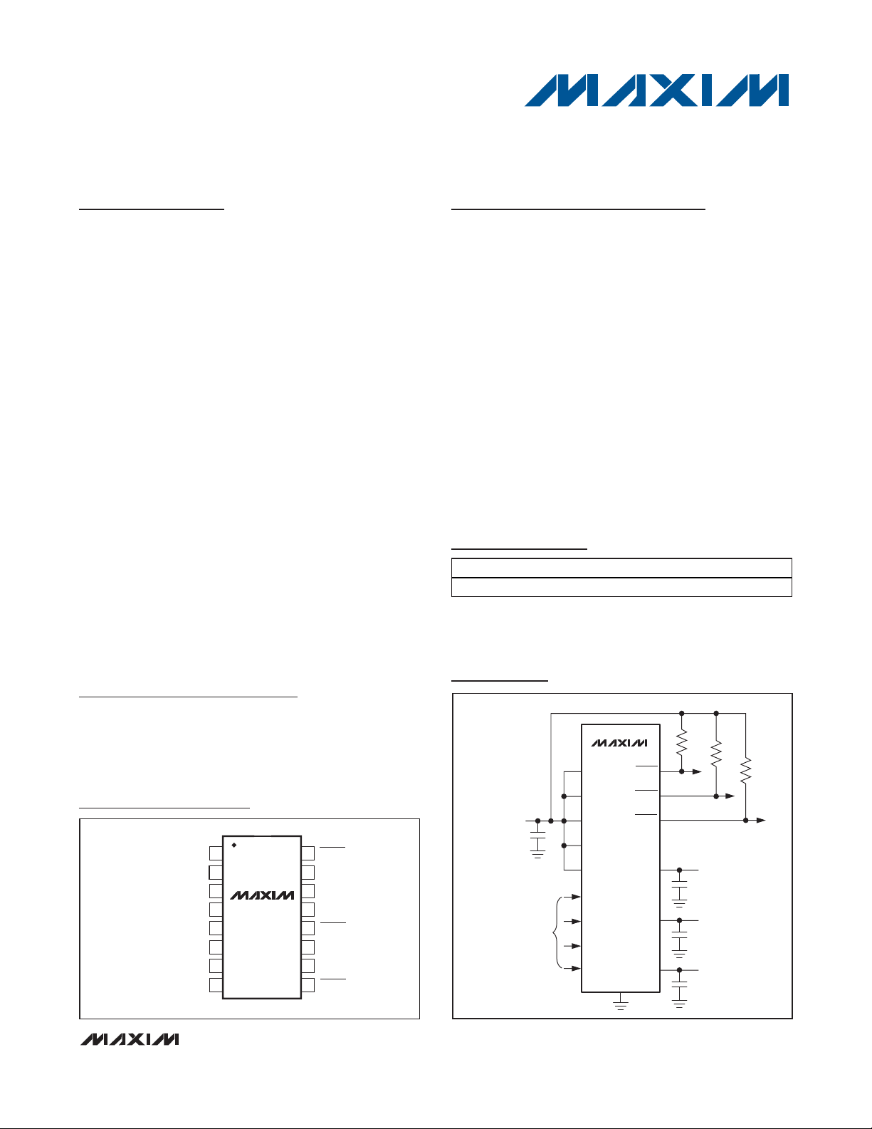
Pin Configuration
USB Ports
USB Hubs
Notebook Computers
Desktop Computers
PDAs and Palmtop
Computers
Docking Stations
PART TEMP RANGE PIN-PACKAGE
MAX1940EEE -40°C to +85°C 16 QSOP
TOP VIEW
ONA
1
IN1
2
IN2
3
4
IN3
ONB
5
IN4
6
IN5
7
ONC
8
16
FAULTA
15
OUTA
14
GND
MAX1940
QSOP
13
12
11
10
9
OUTB
FAULTB
SEL
OUTC
FAULTC
INPUT
4V TO 5.5V
ACTIVE-HIGH/ACTIVE-LOW
SELECTABLE
MAX1940
IN1
IN2
IN3
IN4
IN5
ONA
ONB
ONC
SEL
FAULTA
FAULTB
FAULTC
OUTA
OUTB
OUTC
GND
USB
PORT A
USB
PORT B
USB
PORT C
Page 2
MAX1940
Triple USB Switch with Autoreset and
Fault Blanking
2 _______________________________________________________________________________________
ABSOLUTE MAXIMUM RATINGS
Stresses beyond those listed under “Absolute Maximum Ratings” may cause permanent damage to the device. These are stress ratings only, and functional
operation of the device at these or any other conditions beyond those indicated in the operational sections of the specifications is not implied. Exposure to
absolute maximum rating conditions for extended periods may affect device reliability.
IN_, ON_, OUT_, SEL, FAULT_, to GND...................-0.3V to +6V
IN1, IN2 to OUTA......................................................-0.3V to +6V
IN2, IN3 to OUTB......................................................-0.3V to +6V
IN4, IN5 to OUTC .....................................................-0.3V to +6V
OUT_ Continuous Switch Current
(per channel, internally limited).........................................1.4A
FAULT_ DC Current ............................................................20mA
Continuous Power Dissipation (T
A
= +70°C)
16-Pin QSOP (derate 8.3mW/°C above +70°C)...........667mW
Operating Temperature Range ...........................-40°C to +85°C
Junction Temperature......................................................+150°C
Storage Temperature Range .............................-65°C to +150°C
Lead Temperature (soldering, 10s) .................................+300°C
ELECTRICAL CHARACTERISTICS
(V
IN_
= 5V, C
IN_
= 0.1µF, C
OUT_
= 1µF, TA= 0°C to +85°C, unless otherwise noted. Typical values are at TA= +25°C.)
Supply Voltage Range V
Switch On-Resistance R
Standby Supply Current All switches disabled 3 10 µA
OUT_ Off-Leakage Current I
Undervoltage Lockout Threshold V
Continuous Load Current 500 mA
Continuous Current Limit I
Short-Circuit Current Limit I
Short-Circuit Detect Threshold (Note 1) 1 V
Continuous Current-Limit
Blanking Timeout Period
Short-Circuit Blanking Timeout
Period
Turn-On Delay t
Output Rise Time t
Turn-Off Delay t
Output Fall Time t
Thermal-Shutdown Threshold 15°C hysteresis 160 °C
ON_, SEL Input High Level V
ON_, SEL Input Low Level V
ON_, SEL Input Leakage Current V
PARAMETER SYM B O L CONDITIONS MIN TYP MAX UNITS
IN_
ON
IN_
LKG
ULVO
LIM
SC
TA = 0°C to +85°C, each switch 85 135 mΩ
One switch enabled, I
Two switches enabled, I
All switches enabled, I
All switches disabled, V
T
= 0°C to +85°C
A
= 0 47 75
OUT_
= 0 55 90Quiescent Supply Current I
OUT_
= 0 63 100
OUT_
= 0,
OUT_
Rising edge, 3% hysteresis 3.0 3.4 3.8 V
V
IN_
V
OUT_
- V
= 0.5V 0.7 0.9 1.2 A
OUT_
= 0 (I
OUT_
pulsing)
From continuous current-limit condition to
FAULT_ asserted
From short-circuit current-limit condition to
FAULT_ asserted
R
= 10Ω, does not include rise time
ON
RISE
OFF
FALL
IH
IL
OUT_
(from ON_ to 10% of V
R
= 10Ω, from 10% to 90% of V
OUT_
R
= 10Ω, does not include fall time
OUT_
(from ON_ to 90% of V
R
= 10Ω, from 90% to 10% of V
OUT_
V
= 4V to 5.5V 2 V
IN_
V
= 4V to 5.5V 0.8 V
IN_
= 0 or V
ON_
IN_
OUT_
OUT_
)
OUT_
)
OUT_
4.0 5.5 V
0.02 10 µA
0.9 1.2 1.6 A
0.35 A
10 20 35 ms
7.5 18 35.0 ms
0.5 1.2 4.0 ms
2.5 ms
0.8 3 ms
2.5 ms
-1 +1 µA
µA
PK
RMS
Page 3
MAX1940
Triple USB Switch with Autoreset and
Fault Blanking
_______________________________________________________________________________________ 3
ELECTRICAL CHARACTERISTICS (continued)
(V
IN_
= 5V, C
IN_
= 0.1µF, C
OUT_
= 1µF, TA= 0°C to +85°C, unless otherwise noted. Typical values are at TA= +25°C.)
ELECTRICAL CHARACTERISTICS
(V
IN_
= 5V, C
IN_
= 0.1µF, C
OUT_
= 1µF, TA= -40°C to +85°C, unless otherwise noted.) (Note 2)
Note 1: Short-circuit detect threshold is the output voltage at which the device transitions from short-circuit current limit to
continuous current limit.
Note 2: Specifications to -40°C are guaranteed by design, not production tested.
FAULT_ Output Low Voltage V
FAULT_ Output High Leakage
Current
OUT_ Autoreset Current In latched off state, V
PARAMETER SYM B O L CONDITIONS MIN TYP MAX UNITS
I
OL
SINK
V
IN_
= 1mA, V
= V
FAULT_
= 4V 0.4 V
IN_
= 5.5V 1 µA
= 0 102545mA
OUT_
OUT_ Autoreset Threshold In latched off state, OUT_ rising 0.4 0.5 0.6 V
OUT_ Autoreset Blanking Time In latched off state, V
> 0.5V 10 20 35 ms
OUT_
Supply Voltage Range V
Switch On-Resistance R
Standby Supply Current All switches disabled 10 µA
OUT_ Off-Leakage Current I
Undervoltage Lockout Threshold V
Continuous Load Current 500 mA
Continuous Current Limit I
Short-Circuit Current Limit I
Continuous Current-Limit
Blanking Timeout Period
Short-Circuit Blanking Timeout
Period
Turn-On Delay t
Turn-Off Delay t
ON_, SEL Input High Level V
ON_, SEL Input Low Level V
ON_, SEL Input Leakage Current V
FAULT_ Output Low Voltage V
FAULT_ Output High Leakage
Current
OUT_ Autoreset Current In latched off state, V
OUT_ Autoreset Threshold In latched off state, OUT_ rising 0.4 0.6 V
OUT_ Autoreset Blanking Time In latched off state, V
PARAMETER SYM B O L CONDITIONS MIN MAX UNITS
IN_
ON
IN_
LKG
ULVO
LIM
SC
Each switch 135 mΩ
One switch enabled, I
Two switches enabled, I
All switches enabled, I
All switches disabled, V
= 0 75
OUT_
= 0 90Quiescent Supply Current I
OUT_
= 0 100
OUT_
= 0 10 µA
OUT_
Rising edge, 3% hysteresis 3.0 3.8 V
V
IN_
V
OUT_
- V
= 0.5V 0.7 1.2 A
OUT_
= 0 (I
pulsing) 0.9 1.6 A
OUT_
From continuous current-limit condition to
FAULT_ asserted
From short-circuit current-limit condition to
FAULT_ asserted
R
= 10Ω, does not include rise time
ON
OFF
IH
IL
OL
OUT_
(from ON_ to 10% of V
R
= 10Ω, does not include fall time
OUT_
(from ON_ to 90% of V
V
= 4V to 5.5V 2 V
IN_
V
= 4V to 5.5V 0.8 V
IN_
= 0 or V
ON_
I
SINK
V
IN_
= 1mA, V
= V
IN_
= 4V 0.4 V
IN_
= 5.5V 1 µA
FAULT_
)
OUT_
)
OUT_
= 0 10 50 mA
OUT_
> 0.5V 10 35 ms
OUT_
4.0 5.5 V
10 35 ms
7.5 35.0 ms
0.5 4.0 ms
3ms
-1 +1 µA
µA
PK
Page 4
MAX1940
Triple USB Switch with Autoreset and
Fault Blanking
4 _______________________________________________________________________________________
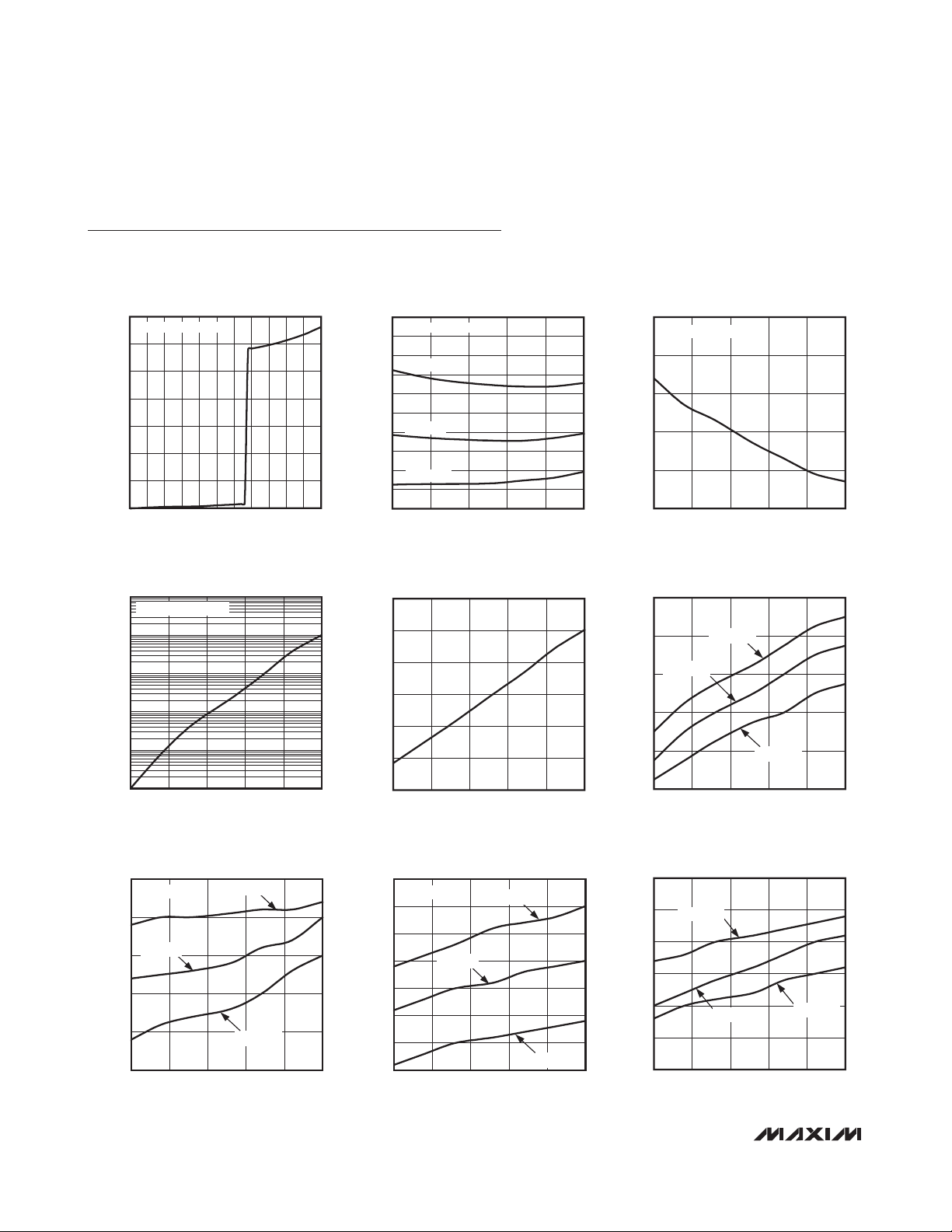
Typical Operating Characteristics
(Circuit of Figure 2, V
IN_
= 5V, C
IN_
= 0.1µF, C
OUT_
= 1µF, ON_ = SEL, TA= +25°C, unless otherwise noted.)
QUIESCENT SUPPLY CURRENT
vs. INPUT VOLTAGE
MAX1940 toc01
INPUT VOLTAGE (V)
QUIESCENT SUPPLY CURRENT (µA)
5.04.54.03.53.02.52.01.51.00.5
10
20
30
40
50
60
70
0
05.5
ALL SWITCHES ACTIVE
QUIESCENT SUPPLY CURRENT
vs. TEMPERATURE
MAX1940 toc02
TEMPERATURE (°C)
QUIESCENT SUPPLY CURRENT (µA)
603510-15
61
62
63
64
65
66
67
68
69
70
60
-40 85
ALL SWITCHES ACTIVE
V
IN_
= 5.5V
V
IN_
= 5V
V
IN_
= 4.5V
SHUTDOWN SUPPLY CURRENT
vs. TEMPERATURE
MAX1940 toc03
TEMPERATURE (°C)
SHUTDOWN SUPPLY CURRENT (µA)
603510-15
2.6
2.7
2.8
2.9
3.0
2.5
-40 85
ON_ = GND, V
SEL
= 5V
SWITCH OFF-LEAKAGE (ONE SWITCH)
vs. TEMPERATURE
MAX1940 toc04
TEMPERATURE (°C)
SWITCH OFF-LEAKAGE (nA)
603510-15
0.1
1
10
100
1000
0.01
-40 85
ON_ = OUT_, V
SEL
= 5V
CONTINUOUS CURRENT-LIMIT THRESHOLD
vs. TEMPERATURE
MAX1940 toc06
TEMPERATURE (°C)
CONTINUOUS CURRENT-LIMIT THRESHOLD (mA)
603510-15
904
908
912
916
920
900
-40 85
V
IN_
= 5.0V
V
IN_
= 5.5V
V
IN_
= 4.5V
FAULT-BLANKING TIME
vs. TEMPERATURE
MAX1940 toc09
TEMPERATURE (°C)
FAULT-BLANKING TIME (ms)
603510-15
19.5
20.0
20.5
21.0
21.5
22.0
19.0
-40 85
V
IN_
= 5.5V
V
IN_
= 5V
V
IN_
= 4.5V
NORMALIZED ON-RESISTANCE
1.3
vs. TEMPERATURE
TURN-ON TIME (tON + t
RISE
)
vs. TEMPERATURE
3.5
R
= 10Ω
OUT_
3.4
V
= 5V
IN_
3.3
3.2
TURN-ON TIME (ms)
3.1
3.0
-40 85
V
= 4.5V
IN_
V
IN_
TEMPERATURE (°C)
MAX1940 toc07
= 5.5V
603510-15
1.2
1.1
1.0
0.9
NORMALIZED ON-RESISTANCE
0.8
0.7
-40 85
TEMPERATURE (°C)
TURN-OFF TIME (t
OFF
+ t
vs. TEMPERATURE
3.3
R
= 10Ω
OUT_
3.2
3.1
3.0
2.9
TURN-OFF TIME (ms)
2.8
2.7
2.6
-40 85
V
V
IN_
= 5V
IN_
TEMPERATURE (°C)
= 5.5V
V
603510-15
FALL
IN_
603510-15
MAX1940 toc05
)
MAX1940 toc08
= 4.5V
Page 5

MAX1940
Triple USB Switch with Autoreset and
Fault Blanking
_______________________________________________________________________________________
5
Typical Operating Characteristics (continued)
(Circuit of Figure 2, V
IN_
= 5V, C
IN_
= 0.1µF, C
OUT_
= 1µF, ON_ = SEL, TA= +25°C, unless otherwise noted.)
FAULT OUTPUT LOW VOLTAGE
vs. TEMPERATURE
250
RPU = 4.7kΩ
240
230
220
V
210
200
190
180
170
160
150
140
130
FAULT OUTPUT LOW VOLTAGE (mV)
120
110
100
= 5.5V
IN_
-40 85
V
= 5V
IN_
V
IN_
TEMPERATURE (°C)
OVERLOAD RESPONSE INTO 2.5Ω
A
B
C
D
10ms/div
5V/div
C: V
D: I
FAULT_
OUT_
A: V
B: V
IN_
OUT_
5V/div
SHORT-CIRCUIT RESPONSE INTO 0Ω
(EXPANDED TIME SCALE)
A
B
C
= 4.5V
5V/div
1A/div
603510-15
MAX1940 toc13
MAX1940 toc16
AUTORESET CURRENT
vs. INPUT VOLTAGE
TA = -40°C
TA = +25°C
TA = +85°C
INPUT VOLTAGE (V)
SHORT-CIRCUIT RESPONSE INTO 0Ω
5V/div
10ms/div
C: V
FAULT_
D: I
OUT_
1A/div
A: V
B: V
IN_
OUT_
5V/div
SWITCH TURN-ON TIME (tON + t
V
= 5V
SEL
= 10Ω
R
OUT_
= 1µF
C
OUT_
38
36
MAX1940 toc10
34
32
30
28
26
24
AUTORESET CURRENT (mA)
22
20
18
5V
0
0
0
5V
0
5V
A
B
C
D
A
B
AUTORESET CURRENT
vs. TEMPERATURE
V
= 5.5V
IN_
V
= 5V
IN_
V
= 4.5V
IN_
-40 85
TEMPERATURE (°C)
603510-15
OVERLOAD RESPONSE INTO 2.5Ω
(EXPANDED TIME SCALE)
400µs/div
5V/div
C: V
D: I
FAULT_
OUT_
1A/div
A: V
B: V
IN_
OUT_
5V/div
SWITCH TURN-ON TIME (tON + t
V
= 5V
SEL
= 10Ω
R
OUT_
= 1µF
C
OUT_
5V/div
MAX1940 toc14
RISE
MAX1940 toc17
)
40
35
MAX1940 toc11
30
25
20
15
AUTORESET CURRENT (mA)
10
5
0
3.5 5.5
5V
0
5V
0
5V
5V
A
B
C
D
A
B
5V/div
MAX1940 toc15
FALL
MAX1940 toc18
MAX1940 toc12
5.35.13.7 3.9 4.1 4.5 4.74.3 4.9
5V
5V
5V
0
)
5V
D
400µs/div
5V/div
C: V
D: I
FAULT_
IN_
2A/div
5V/div
A: V
B: V
IN_
OUT_
5V/div
0
A: V
5V/div
ON_
2V/div
B: V
OUT_
1ms/div
A: V
B: V
ON_
OUT_
5V/div
2V/div
1ms/div
0
Page 6

MAX1940
Triple USB Switch with Autoreset and
Fault Blanking
6 _______________________________________________________________________________________
Typical Operating Characteristics (continued)
(Circuit of Figure 2, V
IN_
= 5V, C
IN_
= 0.1µF, C
OUT_
= 1µF, ON_ = SEL, TA= +25°C, unless otherwise noted.)
SEL
ON_
FAULT_
= 5V, R
5V/div
STARTUP TIME
= 330µF
C
OUT
= 10Ω, C
OUT_
1ms/div
C: V
5V/div
D: I
OUT_
OUT_
= 330µF
OUT_
5V/div
500mA/div
MAX1940 toc20
5V
5V
0
500mA
STARTUP TIME
= 1µF
C
OUT
V
= 5V, R
SEL
A
B
C
D
A: V
ON_
B: V
FAULT_
5V/div
5V/div
OUT_
= 10Ω, C
400µs/div
C: V
OUT_
D: I
OUT_
= 1µF
OUT_
5V/div
500mA/div
MAX1940 toc19
5V
5V
5V
500mA
V
A
B
C
D
A: V
B: V
STARTUP TIME
= 100µF
C
OUT
V
= 5V, R
SEL
A
B
C
D
A: V
ON_
B: V
FAULT_
5V/div
5V/div
OUT_
= 10Ω, C
1ms/div
C: V
OUT_
D: I
OUT_
= 100µF
OUT_
2V/div
500mA/div
MAX1940 toc21
5V
5V
5V
500mA
UNDERVOLTAGE LOCKOUT RESPONSE
R
= 10Ω, C
OUT_
A
B
C
5V/div
A: V
IN_
5V/div
B: V
OUT_
OUT_
10ms/div
C: V
= 1µF
FAULT_
5V/div
MAX1940 toc22
0
0
0
Page 7

MAX1940
Triple USB Switch with Autoreset and
Fault Blanking
_______________________________________________________________________________________ 7
Pin Description
PIN NAME FUNCTION
1 ONA Control Input for Switch A. The active polarity of ONA is set by SEL (see Table 1).
2 IN1
3 IN2
4 IN3
5 ONB Control Input for Switch B. The active polarity of ONB is set by SEL (see Table 1).
6 IN4
7 IN5
8 ONC Control Input for Switch C. The active polarity of ONC is set by SEL (see Table 1).
9 FAULTC
10 OUTC
11 SEL
12 FAULTB
13 OUTB
14 GND Ground
15 OUTA
16 FAULTA
Power Input. Connect all IN_ inputs together and bypass with a 0.1µF ceramic capacitor to GND. Load
conditions might require additional bulk capacitance to prevent pulling IN_ down.
Power Input. Connect all IN_ inputs together and bypass with a 0.1µF ceramic capacitor to GND. Load
conditions might require additional bulk capacitance to prevent pulling IN_ down.
Power Input. Connect all IN_ inputs together and bypass with a 0.1µF ceramic capacitor to GND. Load
conditions might require additional bulk capacitance to prevent pulling IN_ down.
Power Input. Connect all IN_ inputs together and bypass with a 0.1µF ceramic capacitor to GND. Load
conditions might require additional bulk capacitance to prevent pulling IN_ down.
Power Input. Connect all IN_ inputs together and bypass with a 0.1µF ceramic capacitor to GND. Load
conditions might require additional bulk capacitance to prevent pulling IN_ down.
Fault Indicator Output for Switch C. Open-drain output asserts low when switch C enters thermal shutdown,
undervoltage lockout, or a sustained (>20ms) current-limit or short-circuit condition.
Power Output for Switch C. Bypass OUTC to GND with a 1µF ceramic capacitor. Load conditions might
require additional bulk capacitance. When disabled, OUTC goes into a high-impedance state.
Logic Input Polarity Select. SEL sets the active polarity of the ON_ inputs. Connect SEL high to set activehigh inputs. Connect SEL to GND to set active-low inputs.
Fault Indicator Output for Switch B. Open-drain output asserts low when switch B enters thermal shutdown,
undervoltage lockout, or enters a sustained (>20ms) current-limit or short-circuit condition.
Power Output for Switch B. Bypass OUTB to GND with a 1µF ceramic capacitor. Load conditions might
require additional bulk capacitance. When disabled, OUTB goes into a high-impedance state.
Power Output for Switch A. Bypass OUTA to GND with a 1µF ceramic capacitor. Load conditions might
require additional bulk capacitance. When disabled, OUTA goes into a high-impedance state.
Fault Indicator Output for Switch A. Open-drain output asserts low when switch A enters thermal shutdown,
undervoltage lockout, or a sustained (>20ms) current-limit or short-circuit condition.
Page 8

MAX1940
Detailed Description
The MAX1940 triple current-limited USB power switch
provides three independent switches, each with its own
enable-control input and fault indicator (see Figure 1).
A logic input sets the active polarity of the enable control inputs. The fault indicators notify the system when
the current-limit, short-circuit, undervoltage lockout, or
thermal-shutdown threshold is exceeded.
The MAX1940 operates from a 4V to 5.5V input supply
and supplies a minimum output current of 700mA per
channel. A built-in current limit of 0.9A (typ) limits the
output current in the event of an overload condition.
Built-in short-circuit detection pulses the output current if
the output voltage falls below 1V, resulting in lower RMS
output current and reduced power dissipation in the
device. Independent thermal shutdown allows normal
operation to continue if one channel experiences a prolonged overload or short-circuit condition.
Low-R
ON
NMOS switches enable the MAX1940 to provide three switches in the space-saving 16-pin QSOP
package. An internal micropower charge pump generates the high-side supply needed for driving the gates
of these high-side switches. Separate current-limiting
and thermal-shutdown circuitry permits each switch to
operate independently, improving system robustness.
Triple USB Switch with Autoreset and
Fault Blanking
8 _______________________________________________________________________________________
Figure 1. Functional Diagram
ONA
ONB
IN1
SEL
MAX1940
THERMAL
SHUTDOWN
FAULT LOGIC
20ms TIMERS
UVLO
CHARGE
PUMP
OSC
25kHz
SWITCH B
(SEE SWITCH A)
BIAS
25mA
IN2
ILIM
SWITCH A
(EXPANDED)
SWITCH C
(SEE SWITCH A)
IN_
FAULTA
OUTA
OUTB
FAULTB
OUTC
FAULTC
ONC
REF
IN2 IN3 IN4 IN5GND
Page 9

On/Off Control and
Undervoltage Lockout
SEL sets the active polarity of the logic inputs of the
MAX1940. Connect ON_ to the same voltage as SEL to
enable the respective OUT_ switch. Connect ON_ to
the opposite voltage as SEL to disable the respective
output (see Table 1). The output of a disabled switch
enters a high-impedance state.
The MAX1940 includes a UVLO circuit to prevent erroneous switch operation when the input voltage goes low
during startup and brownout conditions. Input voltages of
less than 3.4V inhibit operation of the device. FAULT_
asserts low during an undervoltage lockout condition.
Output Fault Protection and
Autoreset
The MAX1940 senses the switch output voltage and
selects continuous current limiting for V
OUT_
greater
than 1V, or short-circuit current limiting for V
OUT_
less
than 1V. When V
OUT_
is greater than 1V, the device
operates in a continuous current-limit mode that limits
output current to 0.9A. When V
OUT_
is less than 1V, the
device operates in short-circuit current-limit mode,
sourcing 1.2A pulses to the load. When either fault condition persists for 20ms, the output turns off and its fault
flag is asserted. The output automatically restarts 20ms
after the short or overload is removed.
The MAX1940 detects short-circuit removal by sourcing
25mA from the output and monitoring the output voltage. When the voltage at the output exceeds 0.5V for
20ms, the fault flag resets, the output turns back on,
and the 25mA current source turns off. Active loads are
not expected to have measurable current when supplied with less than 0.5V.
Thermal Shutdown
Independent thermal shutdown for each channel permits normal operation of two switches to continue while
a third experiences a thermal fault. The switch turns off
and the FAULT_ output asserts low immediately when
the junction temperature exceeds +160°C. Thermal
shutdown does not utilize the 20ms fault-blanking timeout period. The switch turns on again and FAULT_
returns high when the junction temperature cools by
+15°C. The switch cycles on and off if the overload
condition persists, resulting in a pulsed output that
reduces system power.
Fault Indicators
The MAX1940 provides an independent open-drain fault
output (FAULT_) for each switch. Connect FAULT_ to IN_
through a 100kΩ pullup resistor for most applications.
FAULT_ asserts low when any of the following conditions
occur:
• The input voltage is below the UVLO threshold.
• The switch junction temperature exceeds the +160°C
thermal-shutdown temperature limit.
• The switch is in current-limit or short-circuit currentlimit mode after the fault-blanking period (20ms)
expires.
The FAULT_ output deasserts after a 20ms delay once
the fault condition is removed. Ensure that the MAX1940
input bypass capacitance prevents glitches from triggering the FAULT_ outputs. Limit the input voltage slew rate
to 0.2V/µs to prevent erroneous FAULT_ indications.
To differentiate large capacitive loads from short circuits or sustained overloads, the MAX1940 has an
independent fault-blanking circuit for each switch.
When a load transient causes the device to enter current limit, an internal counter monitors the duration of
the fault. For load faults exceeding the 20ms faultblanking time, the switch turns off, FAULT_ asserts low,
and the device enters autoreset mode (see the
Output
Fault Protection and Autoreset Mode
section). Only current-limit and short-circuit faults are blanked. Thermal
overload faults and input voltage drops below the
UVLO threshold immediately turn the switch off and
assert FAULT_ low.
Fault blanking allows the MAX1940 to handle USB
loads that might not be fully compliant with USB specifications. The MAX1940 successfully powers USB loads
with additional bypass capacitance and/or large startup currents while protecting the upstream power
source. No fault is reported if the switch brings up the
load within the 20ms blanking period. See Table 2 for a
summary of current-limit and fault behavior.
MAX1940
Triple USB Switch with Autoreset and
Fault Blanking
_______________________________________________________________________________________ 9
Table 1. On/Off Control
SEL ON_ OUT_ BEHAVIOR
GND
V
IN
GND ON
V
IN
GND OFF
V
IN
OFF
ON
Page 10

MAX1940
Applications Information
Input Power Supply and Capacitance
Connect all IN_ inputs together externally. IN_ powers
the internal control circuitry and charge pump for each
switch. Bypass IN_ to GND with a 0.1µF ceramic
capacitor. When driving inductive loads or operating
from inductive sources, which may occur when the
MAX1940 is powered by long leads or PC traces, larger
input bypass capacitance is required to prevent voltage spikes from exceeding the MAX1940’s absolute
maximum ratings during short-circuit events.
Output Capacitor
Bypass OUT_ to GND with a 1µF ceramic capacitor for
local decoupling. Additional bulk capacitance (up to
470µF) reduces output-voltage transients under
dynamic load conditions. Using output capacitors
greater than 470µF might assert FAULT_ if the current
limit cannot charge the output capacitor within the
20ms fault-blanking period. In addition to bulk capacitance, small-value (0.1µF or greater) ceramic capacitors improve the output’s resilience to electrostatic
discharge (ESD).
Driving Inductive Loads
A wide variety of devices (mice, keyboards, cameras,
and printers) typically connect to the USB port with
cables, which might add an inductive component to the
load. This inductance causes the output voltage at the
USB port to oscillate during a load step. The MAX1940
drives inductive loads, but avoid exceeding the
device’s absolute maximum ratings. Usually, the load
inductance is relatively small, and the MAX1940’s input
includes a substantial bulk capacitance from an
upstream regulator as well as local bypass capacitors,
limiting overshoot. If severe ringing occurs because of
large load inductance, clamp the MAX1940 outputs
below +6V and above -0.3V.
Turn-On and Turn-Off Behavior
The MAX1940’s slow turn-on and turn-off minimizes
load transients on the upstream power source. Under
fault conditions, the outputs of the MAX1940 turn off
rapidly to provide maximum safety for the upstream
power source and downstream devices. Internal blocks
shut down to minimize supply current when all three
channels are off.
Layout and Thermal Dissipation
Keep all traces as short as possible to reduce the
effect of undesirable parasitic inductance and optimize
the switch response time to output short-circuit conditions. Place input and output capacitors no more than
5mm from device leads. Connect IN_ and OUT_ to the
Triple USB Switch with Autoreset and
Fault Blanking
10 ______________________________________________________________________________________
Table 2. Current-Limiting and Fault Behavior
CONDITION MAX1940 BEHAVIOR
If a short is detected at the output, the channel turns off, and the blanking timer begins. FAULT_ remains
high during the blanking timeout period.
If the short persists during the fault-blanking period, the output pulses at 0.35A
Output Short Circuit
< 1V)
(V
OUT_
Output Overload Current
> 1V)
(V
OUT_
Thermal Fault
(T
> +160°C)
J
removed before the 18ms short-circuit blanking timeout period, the next ramped current pulse soft-starts
the output. FAULT_ remains high.
If the short circuit persists after the fault-blanking period, FAULT_ goes low, autoreset mode begins, and
the output sources 25mA.
If the output voltage rises above 0.5V for 20ms, the output turns on and FAULT_ goes high (see ShortCircuit Response in the Typical Operating Characteristics.)
Output current regulates at I
blanking timeout period.
Continuous current at I
If overcurrent persists after 20ms, FAULT_ goes low, autoreset mode is enabled, and the output sources
25mA.
If the output voltage rises above 0.5V for 20ms, the output turns on and FAULT_ goes high (see Overload
Response into 2.5Ω in the Typical Operating Characteristics.)
A junction temperature of +160°C immediately asserts FAULT_ low (the blanking timeout period does not
apply for thermal faults) and turns off the switch. When the junction cools by 15°C, the thermal fault is
cleared and FAULT_ goes high. Note that if other fault conditions are present when a thermal fault clears,
those fault states take effect.
LIM
and the blanking timer turns on. FAULT_ remains high during the
LIM
persists until either the 20ms blanking period expires or a thermal fault occurs.
. If the short is
RMS
Page 11

power bus with short traces. Wide power bus planes at
IN_ and OUT provide superior heat dissipation as well.
An active switch dissipates little power with minimal
change in package temperature. Calculate the power
dissipation for this condition as follows:
P = (I
OUT_
)2x R
ON
At the normal operating current (I
OUT_
= 0.5A) and the
maximum on-resistance of the switch (135mΩ), the
power dissipation is:
P = (0.5A)2x 0.135Ω = 34mW per switch.
The worst-case power dissipation occurs when the output
current is just below the current-limit threshold (1.2A max)
with an output voltage greater than 1V. In this case, the
power dissipated in each switch is the voltage drop
across the switch multiplied by the current limit:
P = I
LIM
x (VIN- V
OUT
)
For a 5V input and 1V output, the maximum power dissipation per switch is:
P = 1.2A x (5V - 1V) = 4.8W
Because the package power dissipation is 667mW, the
MAX1940 die temperature exceeds the +160°C thermal
shutdown threshold, and the switch output shuts down
until the junction temperature cools by +15°C. The duty
cycle and period are strong functions of the ambient
temperature and the PC board layout (see the
Thermal
Shutdown
section).
If the output current exceeds the current-limit threshold,
or the output voltage is pulled below the short-circuit
detect threshold, the MAX1940 enters a fault state after
20ms, at which point autoreset mode is enabled and
25mA is sourced by the output. For a 5V input, OUT_
short-circuited to GND, and autoreset mode active, the
power dissipation is as follows:
P = 0.025A x 5V = 0.125W
MAX1940
Triple USB Switch with Autoreset and
Fault Blanking
______________________________________________________________________________________ 11
Figure 2. Typical Application Circuit
100kΩ
MAX1940
IN1
INPUT
4V TO 5.5V
O.1µF
OFF
ON
IN2
IN3
IN4
IN5
ONA
ONB
ONC
SEL
*USB APPLICATIONS MAY REQUIRE
ADDITIONAL BULK CAPACITANCE
FAULTA
FAULTB
FAULTC
OUTA
OUTB
OUTC
GND
100kΩ
100kΩ
USB
PORT A
1µF*
USB
PORT B
1µF*
USB
PORT C
1µF*
Page 12

MAX1940
Triple USB Switch with Autoreset and
Fault Blanking
12 ______________________________________________________________________________________
Chip Information
PROCESS: BiCMOS
Package Information
For the latest package outline information and land patterns, go
to www.maxim-ic.com/packages
. Note that a “+”, “#”, or “-” in
the package code indicates RoHS status only. Package drawings may show a different suffix character, but the drawing pertains to the package regardless of RoHS status.
PACKAGE TYPE PACKAGE CODE DOCUMENT NO.
16 QSOP E16-5
21-0055
Page 13

MAX1940
Triple USB Switch with Autoreset and
Fault Blanking
Maxim cannot assume responsibility for use of any circuitry other than circuitry entirely embodied in a Maxim product. No circuit patent licenses are
implied. Maxim reserves the right to change the circuitry and specifications without notice at any time.
Maxim Integrated Products, 120 San Gabriel Drive, Sunnyvale, CA 94086 408-737-7600 ____________________
13
© 2010 Maxim Integrated Products Maxim is a registered trademark of Maxim Integrated Products, Inc.
Revision History
REVISION
NUMBER
0 7/02 Initial release —
1 2/10 Removed UL Certification Pending bullet from Features section 1
REVISION
DATE
DESCRIPTION
PAGES
CHANGED
 Loading...