

Page 1
General Description
The MAX1937/MAX1938/MAX1939 comprise a family of
synchronous, two-phase, step-down controllers capable
of delivering load currents up to 60A. The controllers utilize Quick-PWM™ control architecture in conjunction with
active load-current voltage positioning. Quick-PWM control provides instantaneous load-step response, while
programmable voltage positioning allows the converter
to utilize full transient regulation limits, reducing the output capacitance requirement. The two phases operate
180° out-of-phase with an effective 500kHz switching frequency, thus reducing input and output current ripple, as
well as reducing input filter capacitor requirements.
The MAX1937/MAX1938/MAX1939 are compliant with
AMD Hammer, Intel®‚ Voltage-Regulator Module (VRM)
9.0/9.1, and AMD Athlon™ Mobile VID code specifications (see Table 1 for VID codes). The internal DAC provides ultra-high accuracy of ±0.75%. A controlled VID
voltage transition is implemented to minimize both
undervoltage and overvoltage overshoot during VID
input change.
Remote sensing is available for high output-voltage
accuracy. The MOSFET switches are driven by a 6V
gate-drive circuit to minimize switching and crossover
conduction losses to achieve efficiency as high as
90%. The MAX1937/MAX1938/MAX1939 feature cycleby-cycle current limit to ensure that the current limit is
not exceeded. Crowbar protection is available to protect against output overvoltage.
Applications
Notebook and Desktop Computers
Servers and Workstations
Blade Servers
High-End Switches
High-End Routers
Macro Base Stations
Features
♦ ±0.75% Output Voltage Accuracy
♦ Instant Load-Transient Response
♦ Up to 90% Efficiency Eliminates Heatsinks
♦ Up to 60A Output Current
♦ 8V to 24V Input Range
♦ User-Programmable Voltage Positioning
♦ Controlled VID Voltage Transition
♦ 500kHz Effective Switching Frequency
♦ MAX1937: AMD Hammer Compatible
♦ MAX1938: Intel VRM 9.0/9.1 Compatible
♦ MAX1939: AMD Athlon Mobile Compatible
♦ Soft-Start
♦ Power-Good (PWRGD) Output
♦ Cycle-by-Cycle Current Limit
♦ Output Overvoltage Protection (OVP)
♦ R
DS(ON)
or R
SENSE
Current Sensing
♦ Remote Voltage Sensing
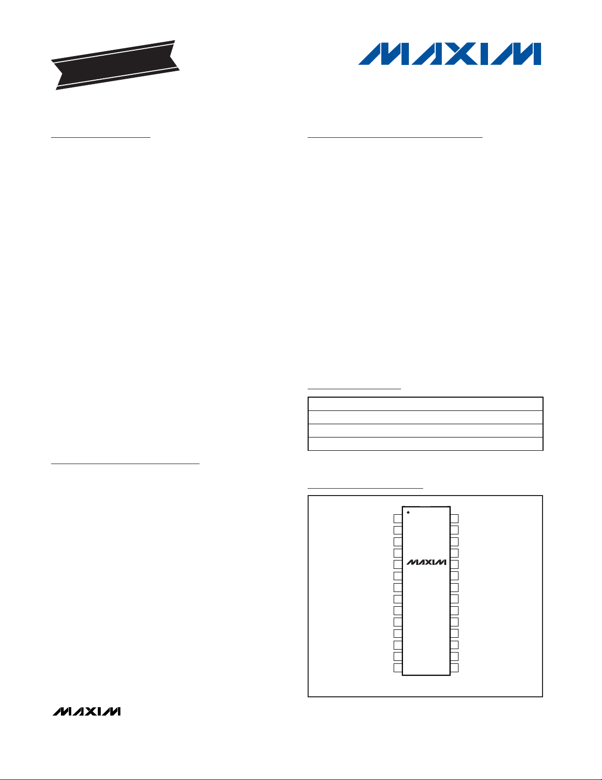
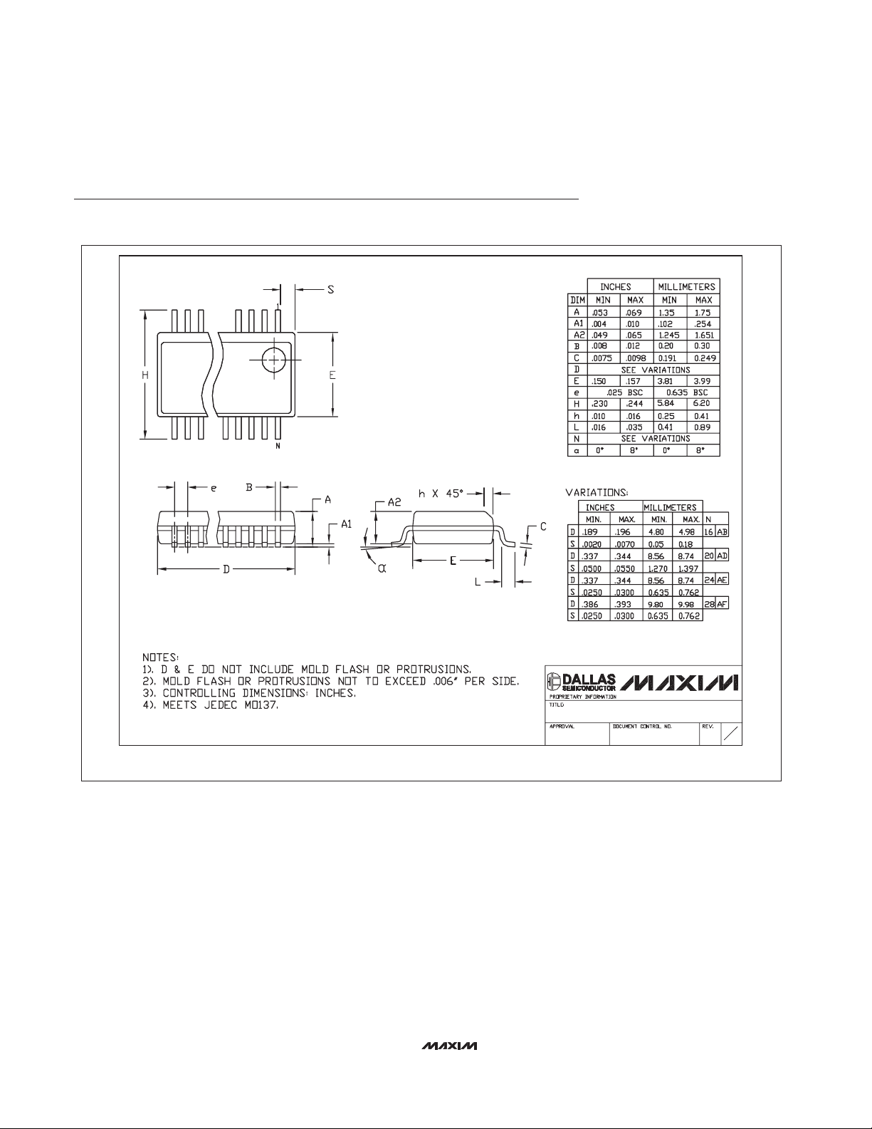
♦ 28-Pin QSOP Package
MAX1937/MAX1938/MAX1939
Two-Phase Desktop CPU Core Supply
Controllers with Controlled VID Change
________________________________________________________________ Maxim Integrated Products 1
28
27
26
25
24
23
22
21
20
19
18
17
16
15
1
2
3
4
5
6
7
8
9
10
11
12
13
14
V
CC
BST1
DH1
LX1
CS1
DL1
PWRGD
VLG
PGND
DL2
CS2
LX2
DH2
BST2
FB
EN
REF
GNDS
GND
ILIM
V
DD
VPOS
VID4
VID3
VID2
TIME
VID1
VID0
QSOP
TOP VIEW
MAX1937
MAX1938
MAX1939
Pin Configuration
Ordering Information
19-2498; Rev 1; 10/02
For pricing, delivery, and ordering information, please contact Maxim/Dallas Direct! at
1-888-629-4642, or visit Maxim’s website at www.maxim-ic.com.
EVALUATION KIT
AVAILABLE
PART TEMP RANGE PIN-PACKAGE
MAX1937EEI -40°C to +85°C 28 QSOP
MAX1938EEI -40°C to +85°C 28 QSOP
MAX1939EEI -40°C to +85°C 28 QSOP
Quick-PWM is a trademark of Maxim Integrated Products, Inc.
Athlon is a trademark of Advanced Micro Devices, Inc.
Intel is a registered trademark of Intel Corp.
Typical Application Circuits and Functional Diagram appear
at end of data sheet.
Page 2
MAX1937/MAX1938/MAX1939
Two-Phase Desktop CPU Core Supply
Controllers with Controlled VID Change
2 _______________________________________________________________________________________
ABSOLUTE MAXIMUM RATINGS
Stresses beyond those listed under “Absolute Maximum Ratings” may cause permanent damage to the device. These are stress ratings only, and functional
operation of the device at these or any other conditions beyond those indicated in the operational sections of the specifications is not implied. Exposure to
absolute maximum rating conditions for extended periods may affect device reliability.
VCCto GND............................................................-0.3V to +28V
V
DD
, PWRGD, ILIM, FB to GND ...............................-0.3V to +6V
EN, GNDS, VPOS, REF, VID_,
TIME to GND ............................................0.3V to V
VDD
+ 0.3V
PGND to GND .......................................................-0.3V to +0.3V
CS1, CS2 to GND ......................................................-2V to +28V
VLG to GND..............................................................-0.3V to +7V
BST1, BST2 to GND ...............................................-0.3V to +35V
LX1 to BST1..............................................................-7V to +0.3V
LX2 to BST2..............................................................-7V to +0.3V
DH1 to LX1.................................................-0.3V to V
BST1
+ 0.3V
DH2 to LX2.................................................-0.3V to V
BST2
+ 0.3V
DL1, DL2 to PGND ......................................-0.3V to V
VLG
+ 0.3V
Continuous Power Dissipation (T
A
= +70°C)
28-Pin QSOP (derate 20.8mW/°C above +70°C)......860.2mW
Operating Temperature Range ...........................-40°C to +85°C
Junction Temperature......................................................+150°C
Storage Temperature Range .............................-65°C to +150°C
Lead Temperature (soldering, 10s) .................................+300°C
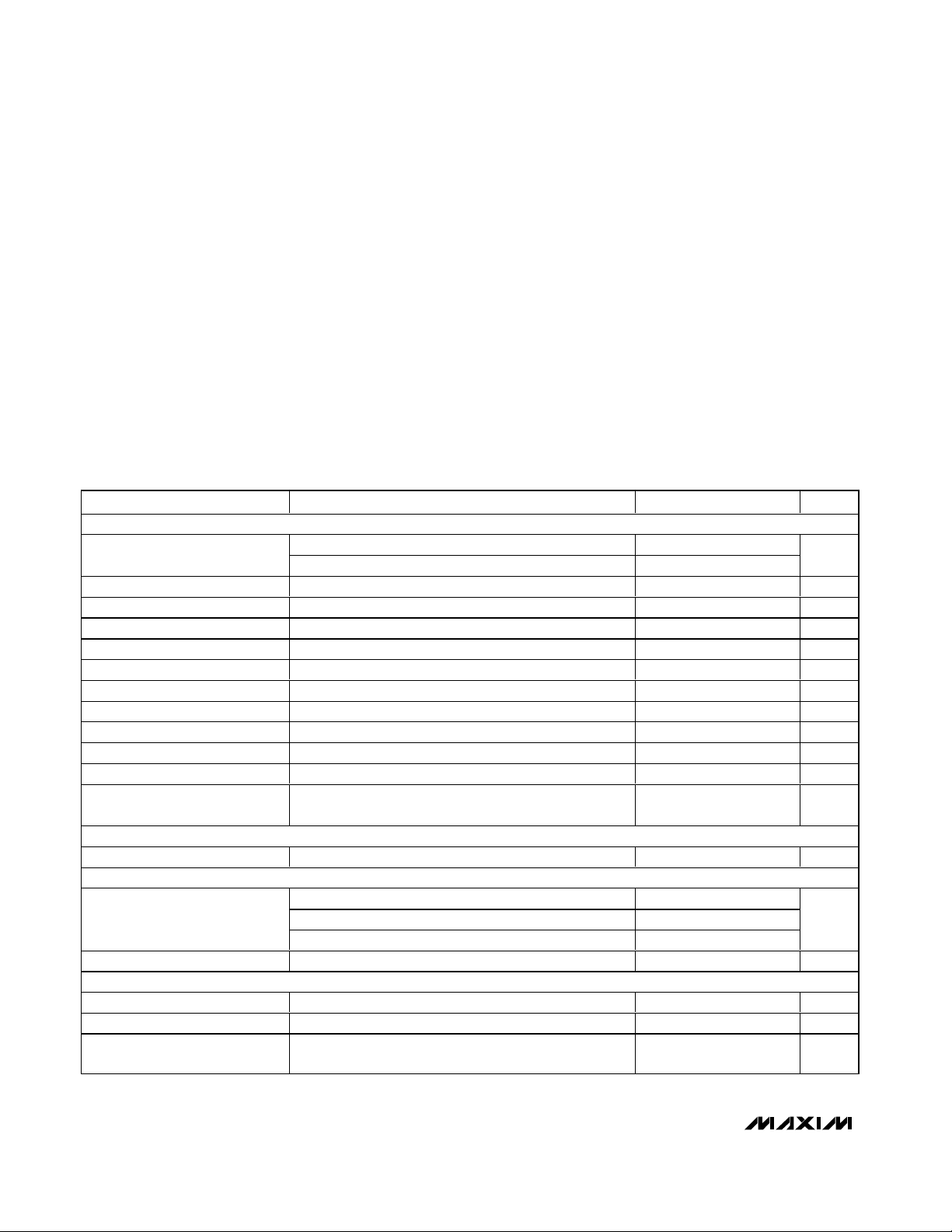
ELECTRICAL CHARACTERISTICS
(VCC= 12V, VEN= V
VDD
= 5V, PGND = GNDS = GND = 0, VID_ = GND, C
VPOS
= 47pF, C
REF
= 0.1µF, V
ILIM
= 1V, TA= 0°C to
+85°C, unless otherwise noted. Typical values are at T
A
= +25°C.)
PARAMETER CONDITIONS
UNITS
GENERAL
MAX1937 6 24
V
CC
Operating Range
MAX1938/MAX1939 8 24
V
V
DD
Operating Range 4.5 5 5.5 V
VLG Operating Range V
VLG
> V
VDD
4.5 6.5 V
V
CC
Operating Supply Current FB above threshold (no switching) 20 40 µA
V
DD
Operating Supply Current FB above threshold (no switching) 1.4 2.5 mA
VLG Operating Supply Current FB above threshold (no switching) 20 60 µA
V
CC
Shutdown Current EN = GND <1 5 µA
V
DD
Shutdown Current EN = GND, VID_ not connected 50
µA
VLG Shutdown Current EN = GND <1 5 µA
TIME Output Voltage
V
ILIM Input Bias V
ILIM
= 1.5V
nA
VPOS Output Voltage
CS_= GND, VPOS connected to REF through a 75kΩ
resistor
2.0
V
REFERENCE
Reference Voltage -50µA ≤ I
REF
≤ 50µA
V
SOFT-START
MAX1937 1.1 5.5
MAX1938 1.5 6.2 Ramp Period
MAX1939 1.3 6.5
ms
Soft-Start Voltage Step 25 mV
ERROR AMPLIFIER
FB Input Resistance Resistance from FB to GND
kΩ
GNDS Input Bias Current -5 +5 µA
Output Regulation Voltage
Accuracy
%
MIN TYP MAX
1.96 2.00 2.04
-250
1.96
100
+250
2.04
1.987 2.000 2.013
180
-0.75
+0.75
Page 3
MAX1937/MAX1938/MAX1939
Two-Phase Desktop CPU Core Supply
Controllers with Controlled VID Change
_______________________________________________________________________________________ 3
ELECTRICAL CHARACTERISTICS (continued)
(VCC= 12V, VEN= V
VDD
= 5V, PGND = GNDS = GND = 0, VID_ = GND, C
VPOS
= 47pF, C
REF
= 0.1µF, V
ILIM
= 1V, TA= 0°C to
+85°C, unless otherwise noted. Typical values are at T
A
= +25°C.)
PARAMETER CONDITIONS
UNITS
FAULT PROTECTION
V
DD
Undervoltage Lockout
(UVLO) Threshold
Rising or falling V
DD
V
V
DD
UVLO Hysteresis 80 mV
VLG UVLO Threshold Rising or falling VLG
V
VLG UVLO Hysteresis 40 mV
Thermal Shutdown Rising temperature, typical hysteresis = 15°C
°C
Rising edge
Reference UVLO Threshold
Falling edge
V
MAX1937/MAX1938
Output Overvoltage Fault
Threshold
MAX1939
V
Output UVLO Threshold
Rising and falling percentage of the nominal
regulation voltage
65 70 75 %
CURRENT LIMIT
PGND to CS_, V
ILIM
= 1.5V
PGND to CS_, V
ILIM
= 1V 90
Current-Limit Threshold
PGND to CS_, V
ILIM
= 0.5V 45 50 55
mV
CS Input Offset Voltage CS_ = GND -3 +3 mV
CS_ Input Bias Current CS_ = GND -5 +5 µA
VOLTAGE POSITIONING
VPOS Input Offset Voltage -3 +3 mV
VPOS Gain
%/V
VPOS Gain
From CS1, CS2 to FB; V
CS1
, V
CS2
= +13mV, -113mV;
R
VPOS
= 75kΩ
68 75 82 %/V
TIMER AND DRIVERS
On-Time LX1 = LX2 = CS1 = CS2 = GND, V
FB
= 1.5V
ns
Minimum Off-Time DH1 low to DH2 high, and DH2 low to DH1 high
ns
MAX1937/MAX1938 60
DH_ low to DL_ high
MAX1939
60
MAX1937/MAX1938 85
Break-Before-Make Time
DL_ low to DH_ high
MAX1939
70
ns
MIN TYP MAX
4.00 4.25 4.45
4.00 4.25 4.45
160
1.600
1.584
Rising and falling
1.97 2.00 2.03
2.215 2.250 2.285
135 150 165
100 110
From CS_ to FB; V
CS1
, V
= 0, -100mV; R
CS2
VPOS
= 75kΩ 72.5 75.0 77.5
420 525 630
260 325 390
Page 4
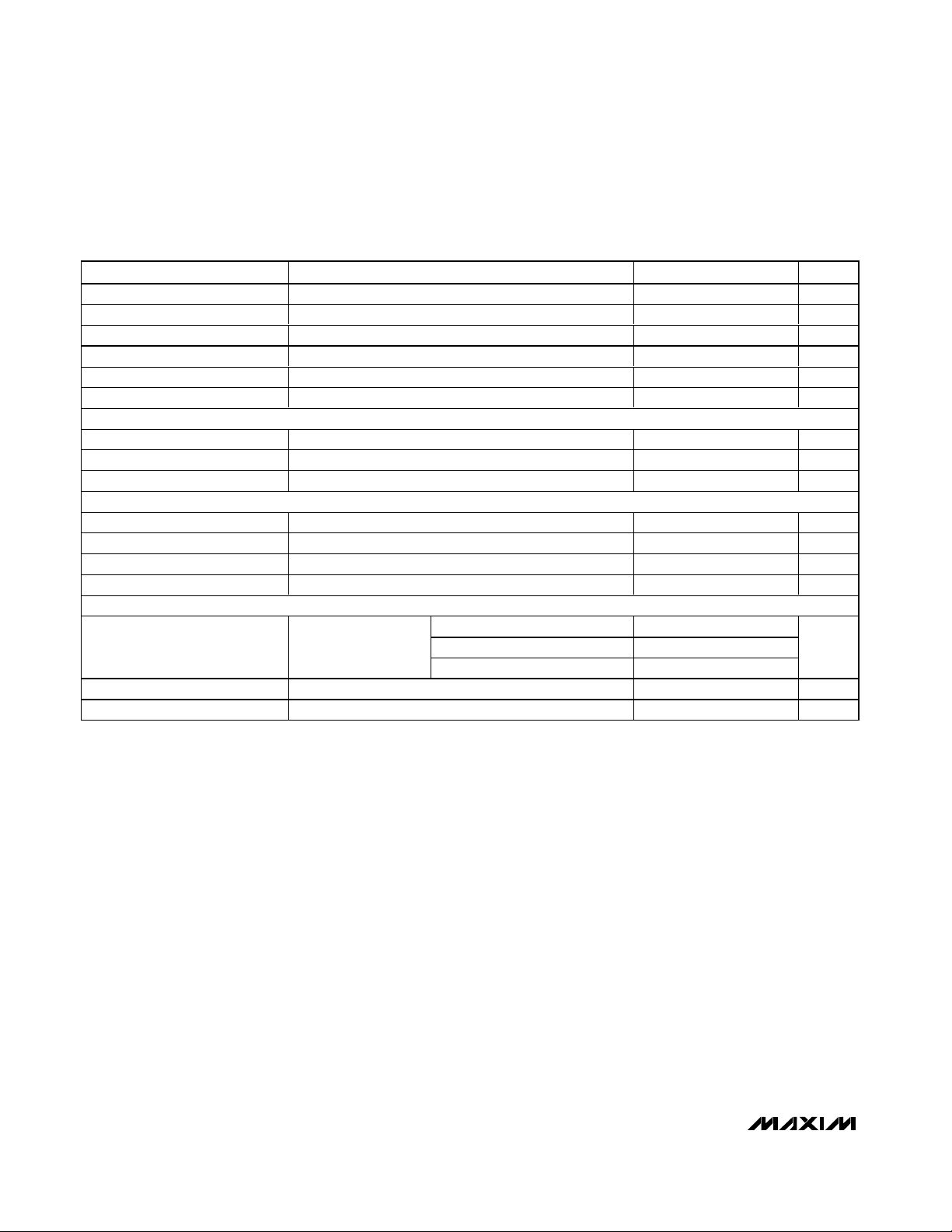
MAX1937/MAX1938/MAX1939
Two-Phase Desktop CPU Core Supply
Controllers with Controlled VID Change
4 _______________________________________________________________________________________
ELECTRICAL CHARACTERISTICS (continued)
(VCC= 12V, VEN= V
VDD
= 5V, PGND = GNDS = GND = 0, VID_ = GND, C
VPOS
= 47pF, C
REF
= 0.1µF, V
ILIM
= 1V, TA= 0°C to
+85°C, unless otherwise noted. Typical values are at T
A
= +25°C.)
PARAMETER CONDITIONS
DH_ On-Resistance in Low State
V
BST1
= V
BST2
= 6V, LX1 = LX2 = GND 1.5 3.0 Ω
DH_ On-Resistance in High State
V
BST_
= 6V, LX_ = GND 1.5 3.0 Ω
DL_ On-Resistance in Low State
0.5 1.7 Ω
DL_ On-Resistance in High State
1.5 3.0 Ω
BST_ Leakage Current V
BST_
= 30V, V
LX_
= 24V 50 µA
LX_ Leakage Current V
BST_
= 30V, V
LX_
= 24V 50 µA
EN AND VID
Low Level Threshold 0.8 V
High Level Threshold 1.6 V
Pullup Resistance Internally pulled up to V
DD
50
kΩ
PWRGD
PWRGD Upper Trip Level
%
PWRGD Lower Trip Level -15
-10 %
Output Low Level 0.4 V
Output High Leakage 1 µA
CONTROLLED VID CHANGE
R
TIME
= 120kΩ
R
TIME
= 47kΩ
On-the-Fly VID Change Slew
Rate
25mV per step
R
TIME
= 470kΩ
µs
VID_ Change Frequency Range
38
kHz
PWRGD Blanking Time V
VDD
= 4.5V to 5.5V
µs
MIN TYP MAX UNITS
10.0 12.5 15.0
100 200
-12.5
6.17 6.67 7.25
2.35 2.63 2.99
23.5 26.3 29.9
380
125 200 350
Page 5
MAX1937/MAX1938/MAX1939
Two-Phase Desktop CPU Core Supply
Controllers with Controlled VID Change
_______________________________________________________________________________________ 5
ELECTRICAL CHARACTERISTICS
(V
VCC
= 12V, VEN= V
VDD
= 5V, PGND = GNDS = GND, VID_= GND, C
VPOS
= 47pF, C
REF
= 0.1µF, V
ILIM
= 1V, TA= -40°C to +85°C,
unless otherwise noted.) (Note 1)
PARAMETER CONDITIONS
UNITS
GENERAL
MAX1937 6 24
V
CC
Operating Range
MAX1938/MAX1939 8 24
V
V
DD
Operating Range 4.5 5.5 V
VLG Operating Range V
VLG
≥ V
VDD
4.5 6.5 V
V
CC
Operating Supply Current FB above threshold (no switching) 40 µA
V
DD
Operating Supply Current FB above threshold (no switching) 2.5 mA
VLG Operating Supply Current FB above threshold (no switching) 20 60 µA
V
CC
Shutdown Current EN = GND 5 µA
V
DD
Shutdown Current EN = GND, VID_ not connected
µA
VLG Shutdown Current EN = GND 5 µA
TIME Output Voltage
V
ILIM Input Bias V
ILIM
= 1V
nA
VPOS Output Voltage
CS_ = GND, VPOS connected to REF through a 75kΩ
resistor
V
REFERENCE
Reference Voltage -50µA ≤ I
REF
≤ 50µA
V
SOFT-START
MAX1937 1.1 5.5
MAX1938 1.5 6.6 Ramp Period
MAX1939 1.3 7.0
ms
ERROR AMPLIFIER
GNDS Input Bias Current -5 +5 µA
Output Regulation Voltage
Accuracy
-1 +1 %
FAULT PROTECTION
V
DD
UVLO Threshold Rising or falling V
DD
V
VLG UVLO Threshold Rising or falling VLG
V
MAX1937/MAX1938
Output Overvoltage Fault
Threshold
MAX1939
V
Output UVLO Threshold
Rising and falling percentage of the nominal
regulation voltage
65 75 %
CURRENT LIMIT
PGND to CS_, V
ILIM
= 1.5V
PGND to CS_, V
ILIM
= 1V 90
Current-Limit Threshold
PGND to CS_, V
ILIM
= 0.5V 45 55
mV
MIN TYP MAX
1.96
-250
1.96
1.98
100
2.04
+250
2.04
2.02
Rising and falling
4.00
4.00
1.97
2.215
135
4.45
4.45
2.03
2.285
165
110
Page 6
MAX1937/MAX1938/MAX1939
Two-Phase Desktop CPU Core Supply
Controllers with Controlled VID Change
6 _______________________________________________________________________________________
ELECTRICAL CHARACTERISTICS (continued)
(V
VCC
= 12V, VEN= V
VDD
= 5V, PGND = GNDS = GND, VID_= GND, C
VPOS
= 47pF, C
REF
= 0.1µF, V
ILIM
= 1V, TA= -40°C to +85°C,
unless otherwise noted.) (Note 1)
PARAMETER CONDITIONS
UNITS
CS Input Offset Voltage CS_ = GND -5 +5 mV
CS_ Input Bias Current CS_ = GND -5 +5 µA
VOLTAGE POSITIONING
VPOS Input Offset Voltage -5 +5 mV
VPOS Gain
%/V
VPOS Gain
From CS1, CS2 to FB; V
CS1
, V
CS2
= +13mV, -113mV;
R
VPOS
= 75kΩ
68 82 %/V
TIMER AND DRIVERS
On-Time LX1 = LX2 = CS1 = CS2 = GND, V
FB
= 1.5V
ns
Minimum Off-Time DH1 low to DH2 high, and DH2 low to DH1 high
ns
DH_ On-Resistance in Low State
V
BST1
= V
BST2
= 6V, LX1 = LX2 = GND 3 Ω
DH_ On-Resistance in High State
V
BST_
= 6V, LX_ = GND 3 Ω
DL_ On-Resistance in Low State
1.7 Ω
DL_ On-Resistance in High State
3 Ω
BST_ Leakage Current V
BST_
= 30V, V
LX_
= 24V 50 µA
LX_ Leakage Current V
BST_
= 30V, V
LX_
= 24V 50 µA
EN AND VID_
Low Level Threshold 0.8 V
High Level Threshold 1.6 V
Pullup Resistance Internally pulled up to V
DD
50
kΩ
PWRGD
PWRGD Upper Trip Level 10 15 %
PWRGD Lower Trip Level -15 -10 %
Output Low Level 0.4 V
Output High Leakage 1 µA
CONTROLLED VID CHANGE
R
TIME
= 120kΩ
R
TIME
= 47kΩ
On-the-Fly VID Change Slew
Rate
25mV per step
R
TIME
= 470kΩ
µs
VID_ Change Frequency Range
38
kHz
PWRGD Blanking Time V
VDD
= 4.5V to 5.5V
µs
Note 1: Specifications to -40°C are guaranteed by design and not production tested.
MIN TYP MAX
From CS_ to FB; V
CS1
, V
= 0, -100mV; R
CS2
= 75kΩ 72.5
VPOS
420
260
77.5
630
390
200
6.17
2.35
23.5
7.25
2.99
29.9
380
125
350
Page 7
MAX1937/MAX1938/MAX1939
Two-Phase Desktop CPU Core Supply
Controllers with Controlled VID Change
_______________________________________________________________________________________ 7
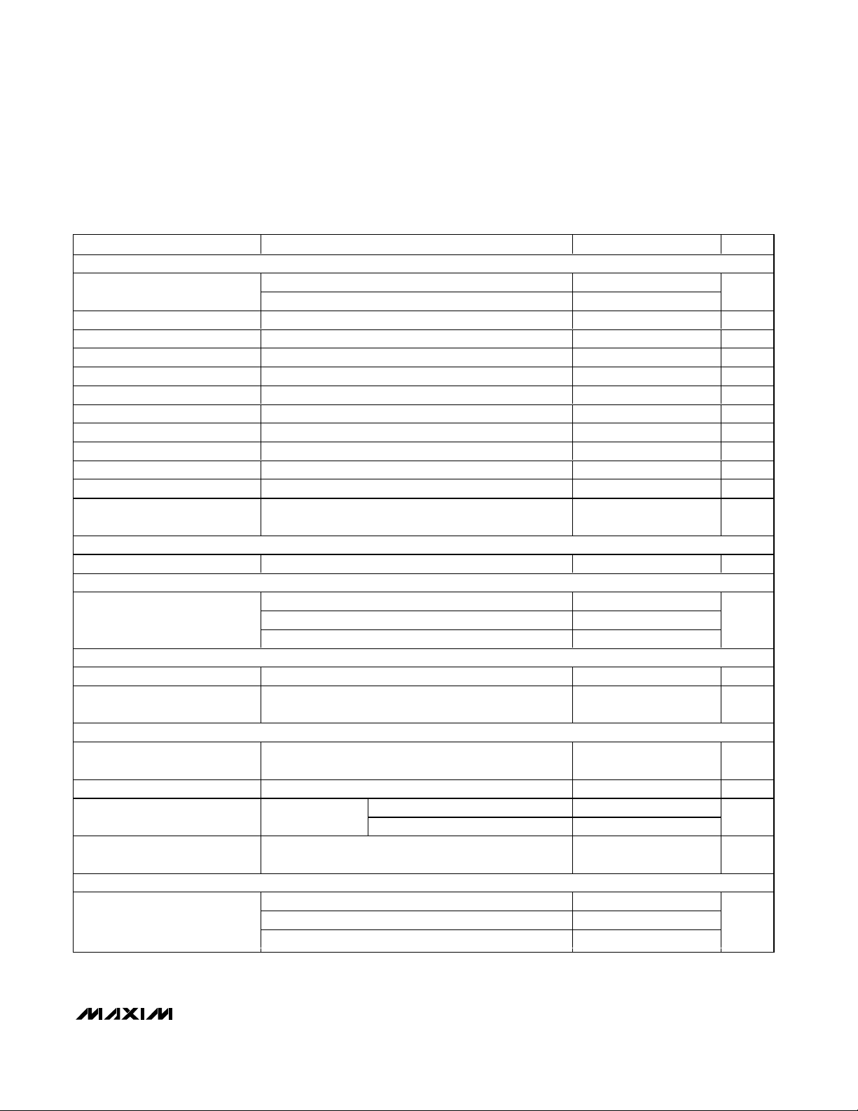
EFFICIENCY vs. LOAD CURRENT
AT 1.45V OUTPUT
MAX1937 toc01
LOAD CURRENT (A)
EFFICIENCY (%)
10
60
70
80
90
50
1 100
VIN = 8V
VIN = 14V
V
IN
= 12V
V
OUT
= 1.45V
50
60
70
80
90
1 10 100
EFFICIENCY vs. LOAD CURRENT
AT 1.85V OUTPUT
MAX1937 toc02
LOAD CURRENT (A)
EFFICIENCY (%)
VIN = 12V
V
IN
= 14V
V
OUT
= 1.85V
V
IN
= 8V
FREQUENCY vs. LOAD CURRENT
MAX1937 toc03
LOAD CURRENT (A)
FREQUENCY (kHz)
5040302010
50
100
150
200
250
300
350
0
060
VIN = 12V
V
OUT
= 1.45V
FREQUENCY vs. INPUT VOLTAGE
MAX1937 toc04
INPUT VOLTAGE (V)
FREQUENCY (kHz)
131211109
175
200
225
250
275
300
325
150
814
I
LOAD
= 46A
V
OUT
= 1.45V
I
LOAD
= 1A
FREQUENCY vs. TEMPERATURE
MAX1937 toc05
TEMPERATURE (°C)
FREQUENCY (kHz)
8060-20 0 20 40
225
230
235
240
245
250
255
260
220
-40 100
VIN = 12V
V
OUT
= 1.45V
I
LOAD
= 10A
VCC INPUT CURRENT
vs. INPUT VOLTAGE
MAX1937 toc06
INPUT VOLTAGE (V)
V
CC
INPUT CURRENT (μA)
131211109
5
10
15
20
25
0
814
V
OUT
= 1.45V
VDD CURRENT vs. VDD VOLTAGE
MAX1937 toc07
V
DD
VOLTAGE (V)
V
DD
CURRENT (mA)
5.35.14.94.7
1.55
1.60
1.65
1.70
1.75
1.80
1.50
4.5 5.5
Typical Operating Characteristics
(VIN= 12V, V
OUT
= 1.45V, TA= +25°C, unless otherwise noted.)
Page 8
MAX1937/MAX1938/MAX1939
Two-Phase Desktop CPU Core Supply
Controllers with Controlled VID Change
8 _______________________________________________________________________________________
Typical Operating Characteristics (continued)
(VIN= 12V, V
OUT
= 1.45V, TA= +25°C, unless otherwise noted.)
CURRENT SHARING
MAX1937 toc10
LOAD CURRENT (A)
INDUCTOR CURRENTS (A)
40302010
0
5
10
15
20
25
30
-5
050
VIN = 12V
V
OUT
= 1.45V
T
A
= +25°C
CURRENT SHARING
MAX1937 toc11
LOAD CURRENT (A)
INDUCTOR CURRENTS (A)
40302010
0
5
10
15
20
25
30
-5
050
VIN = 12V
V
OUT
= 1.45V
T
A
= +80°C
V
IN
= 12V
V
OUT
= 1.45V
I
OUT
= 0A
0A
OUTPUT INDUCTOR
CURRENTS:
10A/div
OUTPUT RIPPLE
VOLTAGE:
20mV/div
2μs/div
MAX1937 toc12
INDUCTOR CURRENT WAVEFORMS
WITH 0A LOAD
V
IN
= 12V
V
OUT
= 1.45V
I
OUT
= 40A
OUTPUT INDUCTOR
CURRENTS:
10A/div
OUTPUT RIPPLE
VOLTAGE:
20mV/div
2μs/div
MAX1937 toc13
INDUCTOR CURRENT WAVEFORMS
WITH 40A LOAD
0A
OUTPUT VOLTAGE vs. LOAD CURRENT
AT 1.45V OUTPUT
MAX1937 toc09
LOAD CURRENT (A)
V
OUT
40302010
1.375
1.400
1.425
1.450
1.350
050
R
VPOS
= 90.9k
Ω
VIN = 12V
R
VPOS
= 120k
Ω
VDD CURRENT vs. VDD VOLTAGE
IN SHUTDOWN
MAX1937 toc08
VDD VOLTAGE (V)
V
DD
CURRENT (mA)
5.35.14.94.7
35
40
45
50
55
65
60
70
30
4.5 5.5
VID_ NOT CONNECTED
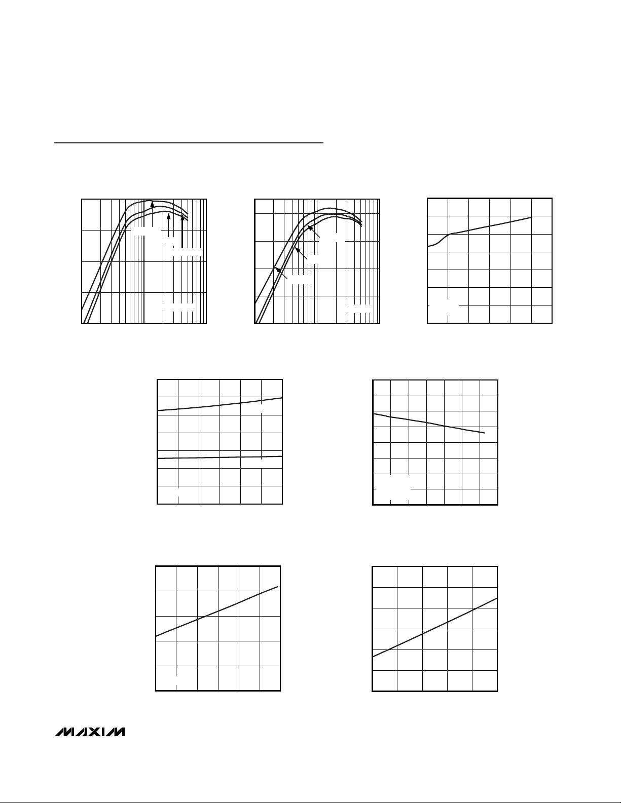
Page 9

ENABLE SIGNAL
OUTPUT VOLTAGE:
0.5V/div
POK SIGNAL
20ms/div
MAX1937 toc18
SHUTDOWN WAVEFORM
WITH 40A LOAD
INDUCTOR CURRENT:
10A/div
MAX1937/MAX1938/MAX1939
Two-Phase Desktop CPU Core Supply
Controllers with Controlled VID Change
_______________________________________________________________________________________ 9
CURRENT-SENSE THRESHOLD vs. V
ILIM
MAX1937 toc19
V
ILIM
(V)
CURRENT-SENSE THRESHOLD (mV)
1.31.10.90.7
60
80
100
120
140
160
40
0.5 1.5
VIN = 12V
V
OUT
= 1.45V
TA = +25°C
TA = +80°C
Typical Operating Characteristics (continued)
(VIN= 12V, V
OUT
= 1.45V, TA= +25°C, unless otherwise noted.)
ENABLE SIGNAL
OUTPUT VOLTAGE:
0.5V/div
POK SIGNAL
1ms/div
MAX1937 toc16
SOFT-START WAVEFORMS
WITH 40A LOAD
INDUCTOR CURRENT:
10A/div
ENABLE SIGNAL
OUTPUT VOLTAGE:
0.5V/div
POK SIGNAL
20ms/div
MAX1937 toc17
SHUTDOWN WAVEFORM
WITH NO LOAD
INDUCTOR CURRENT:
10A/div
40μs/div
MAX1937 toc14
LOAD TRANSIENT
1A TO 40A TO 1A
TRANSIENT CONTROL
SIGNAL:
C6
= 47pF
R2
= 91.1kΩ
INDUCTOR CURRENTS:
10A/div
OUTPUT VOLTAGE:
50mV/div
ENABLE SIGNAL
OUTPUT VOLTAGE:
0.5V/div
POK SIGNAL
1ms/div
MAX1937 toc15
SOFT-START WAVEFORMS
WITH NO LOAD
INDUCTOR CURRENT:
10A/div
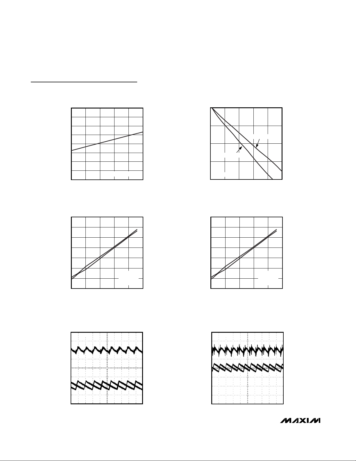
Page 10

MAX1937/MAX1938/MAX1939
Two-Phase Desktop CPU Core Supply
Controllers with Controlled VID Change
10 ______________________________________________________________________________________
REFERENCE VOLTAGE vs. TEMPERATURE
MAX1937 toc22
TEMPERATURE (°C)
REFERENCE VOLTAGE (V)
806040200-20
1.992
1.994
1.996
1.998
2.000
1.990
-40 100
VIN = 12V
V
OUT
= 1.45V
NO LOAD
FB VOLTAGE vs. TEMPERATURE
MAX1937 toc23
TEMPERATURE (°C)
FB VOLTAGE (V)
603510-15
0.795
0.800
0.805
0.810
0.790
-40 85
VIN = 12V
NO LOAD
V
OUT
= 0.8V
FB VOLTAGE vs. TEMPERATURE
MAX1937 toc24
TEMPERATURE (°C)
FB VOLTAGE (V)
806040200-20
1.450
1.455
1.460
1.465
1.445
-40 100
VIN = 12V
NO LOAD
V
OUT
= 1.45V
OUTPUT VOLTAGE:
200mV/div
POK SIGNAL
40
μs/div
MAX1937 toc20
VID CODE CHANGE ON-THE-FLY WITH 40A
LOAD 1.2V TO 1.45V TO 1.2V
VID CODE CHANGE
CONTROL SIGNAL
OUTPUT VOLTAGE:
200mV/div
POK SIGNAL
40μs/div
MAX1937 toc21
VID CODE CHANGE ON-THE-FLY WITH 1A
LOAD 1.2V TO 1.45V TO 1.2V
VID CONTROL
SIGNAL
Typical Operating Characteristics (continued)
(VIN= 12V, V
OUT
= 1.45V, TA= +25°C, unless otherwise noted.)
Page 11

MAX1937/MAX1938/MAX1939
Two-Phase Desktop CPU Core Supply
Controllers with Controlled VID Change
______________________________________________________________________________________ 11
Pin Description
PIN NAME FUNCTION
1 VID0 Voltage Identification Input Bit 0. See Table 1. Internal 100kΩ pullup resistor to V
DD
.
2 VID1 Voltage Identification Input Bit 1. See Table 1. Internal 100kΩ pullup resistor to V
DD
.
3 TIME Connect to an external resistor (47kΩ to 470kΩ) for VID change slew-rate control.
4 VID2 Voltage Identification Input Bit 2. See Table 1. Internal 100kΩ pullup resistor to V
DD
.
5 VID3 Voltage Identification Input Bit 3. See Table 1. Internal 100kΩ pullup resistor to V
DD
.
6 VID4 Voltage Identification Input Bit 4. See Table 1. Internal 100kΩ pullup resistor to V
DD
.
7 VPOS
Voltage Positioning. Connect a resistor between VPOS and REF to set the output voltage-positioning
droop, or connect directly to REF for no output voltage positioning. Connect a 47pF capacitor from
VPOS to GND.
8 V
DD
IC Analog Power-Supply Input. Connect a 5V supply to V
DD
.
9 ILIM
Current-Limit Threshold per Phase. Connect ILIM to V
DD
to set a default current limit of 120mV, or
connect to a voltage-divider from REF to GND to adjust the current limit. See the Setting the Current
Limit section.
10 GND Ground
11 GNDS
Remote Ground Sense. Connect GNDS to the output ground at the load. For VRM applications, also
connect a 100Ω resistor from GNDS to PGND locally.
12 REF Reference Output. Connect a 0.1µF capacitor from REF to GND.
13 EN Enable Input. Leave unconnected or drive high for normal operation. Drive low for shutdown.
14 FB
Remote Feedback Sense. Connect FB to the output at the load. For VRM applications, also connect
a 100Ω resistor from FB to the output locally.
15 PWRGD
Power-Good Output. Open-drain output is high impedance when the output is in regulation and
pulled low when the output deviates more than 12.5% from the voltage set by the VID code. PWRGD
is also low in shutdown or during any fault condition. To use as a logic output, connect a pullup
resistor from PWRGD to the logic supply.
16 BST2
High-Side MOSFET Gate-Driver Bootstrap Input. Connect 0.22µF or higher value bypass capacitor
from BST2 to LX2. Keep trace length as short as possible. Connect a Schottky diode between BST2
and VLG. See the Selecting a BST Capacitor section.
17 DH2
High-Side MOSFET Gate-Drive Output. Connect to the high-side MOSFET gate. DH2 is pulled low in
shutdown.
18 LX2 Inductor Connection. Connect to the switched side of the inductor.
19 CS2
Negative Current-Sense Input. Connect to a current-sense resistor in series with the low-side
MOSFET, or connect to LX2 to use the low-side MOSFET’s on-resistance for current sensing.
20 DL2
Low-Side MOSFET Gate-Driver Output. Connect to the low-side MOSFET gate. DL2 is pulled low in
shutdown.
21 PGND
Power Ground. Connect to power ground at the point where the current-sense resistors or low-side
MOSFET sources connect. PGND is used as the positive current-sense connection.
Page 12

MAX1937/MAX1938/MAX1939
Two-Phase Desktop CPU Core Supply
Controllers with Controlled VID Change
12 ______________________________________________________________________________________
Detailed Description
The MAX1937/MAX1938/MAX1939 is a family of synchronous, two-phase step-down controllers capable of
delivering load currents up to 60A. The controllers use
Quick-PWM control architecture in conjunction with
active load current voltage positioning. Quick-PWM
control provides instantaneous load-step response,
while programmable voltage positioning allows the converter to utilize full transient regulation limits, reducing
the output capacitance requirement. Furthermore, the
two phases operate 180° out-of-phase with an effective
500kHz switching frequency, thus reducing input and
output current ripple, as well as reducing input filter
capacitor requirements.
The MAX1937/MAX1938/MAX1939 are compliant with
the AMD Hammer, Intel VRM 9.0/VRM 9.1, and AMD
Athlon Mobile VID code specifications (see Table 1 for
VID codes). The internal DAC provides ultra-high accuracy of ±0.75%. A controlled VID voltage transition is
implemented to minimize both undervoltage and overvoltage overshoot during VID input change.
Remote sensing is available for high output-voltage
accuracy. The MOSFET switches are driven by with a
6V gate-drive circuit to minimize switching and
crossover conduction losses to achieve efficiency as
high as 90%. The MAX1937/MAX1938/ MAX1939 feature cycle-by-cycle current limit to ensure current limit
is not exceeded. Crowbar protection is available to protect against output overvoltage.
On-Time One-Shot
The heart of the Quick-PWM core is the one-shot that
sets the high-side switch on-time. This fast, low-jitter,
one-shot circuitry varies the on-time in response to the
input and output voltages. The high-side switch on-time
is inversely proportional to the voltage applied to V
CC
and directly proportional to the output voltage. This
algorithm results in a nearly constant switching frequency, despite the lack of a fixed-frequency clock
generator. The benefits of a constant switching frequency are twofold: the frequency selected avoids
noise-sensitive regions, and the inductor ripple current
operating point remains relatively constant, resulting in
easy design methodology and predictable output voltage ripple:
where the constant K is 4µs and V
DROP
is the voltage
drop across the low-side MOSFET’s on-resistance plus
the drop across the current-sense resistor (V
DROP
≈
75mV), if used.
The on-time one-shot has good accuracy at the operating point specified in the Electrical Characteristics. Ontimes at operating points far removed from the
conditions specified in the Electrical Characteristics can
vary over a wide range. For example, the regulators run
slower with input voltages greater than 12V because of
the very short on-times required.
t
KV V
V
ON
OUT DROP
VCC
=
+
()
Pin Description (continued)
PIN NAME FUNCTION
22 VLG
DL_ Driver Power-Supply Input. Connect to a 4.5V to 6.5V supply for powering the low-side MOSFET
gate drive, and the bootstrap circuit for driving the high-side MOSFETs. Ensure that V
VLG
is greater
than or equal to V
VDD
.
23 DL1
Low-Side MOSFET Gate-Driver Output. Connect to the low-side MOSFET gate. DL1 is pulled low in
shutdown.
24 CS1
Negative Current-Sense Input. Connect to a current-sense resistor in series with the low-side
MOSFET or connect to LX1 to use the low-side MOSFET’s on-resistance for current sensing.
25 LX1 Inductor Connection. Connect to the switched side of the inductor.
26 DH1
High-Side MOSFET Gate-Drive Output. Connect to the high-side MOSFET gate. DH1 is pulled low in
shutdown.
27 BST1
High-Side MOSFET Gate-Driver Bootstrap Input. Connect 0.22µF or higher value bypass capacitor
from BST1 to LX1. Keep trace length as short as possible. Connect a Schottky diode between BST1
and VLG. See the Selecting a BST Capacitor section.
28 V
CC
Input Voltage Sense. Connect to the input supply at the high-side MOSFET drain. The voltage
sensed at V
CC
is used to set the on-time.
Page 13

MAX1937/MAX1938/MAX1939
Two-Phase Desktop CPU Core Supply
Controllers with Controlled VID Change
______________________________________________________________________________________ 13
While the on-time is set by the input and output voltage,
other factors contribute to the switching frequency. The
on-time guaranteed in the Electrical Characteristics is
influenced by switching delays in the external high-side
MOSFET. Resistive losses in the inductor, both MOSFETs,
output capacitor ESR, and PC board copper losses in
the output and ground, tend to raise the switching frequency at higher output currents. Switch dead-time can
also increase the effective on-time, reducing the
switching frequency. This effect occurs when the
inductor current reverses at light or negative load currents. With reversed inductor current, the inductor’s
V
OUT
(V)
VID4 VID3 VID2 VID1 VID0
MAX1937 MAX1938 MAX1939
00000 1.550 1.850 2.000
00001 1.525 1.825 1.950
00010 1.500 1.800 1.900
00011 1.475 1.775 1.850
00100 1.450 1.750 1.800
00101 1.425 1.725 1.750
00110 1.400 1.700 1.700
00111 1.375 1.675 1.650
01000 1.350 1.650 1.600
01001 1.325 1.625 1.550
01010 1.300 1.600 1.500
01011 1.275 1.575 1.450
01100 1.250 1.550 1.400
01101 1.225 1.525 1.350
01110 1.200 1.500 1.300
01111 1.175 1.475 Shutdown
10000 1.150 1.450 1.275
10001 1.125 1.425 1.250
10010 1.100 1.400 1.225
10011 1.075 1.375 1.200
10100 1.050 1.350 1.175
10101 1.025 1.325 1.150
10110 1.000 1.300 1.125
10111 0.975 1.275 1.100
11000 0.950 1.250 1.075
11001 0.925 1.225 1.050
11010 0.900 1.200 1.025
11011 0.875 1.175 1.000
11100 0.850 1.150 0.975
11101 0.825 1.125 0.950
11110 0.800 1.100 0.925
11111 Shutdown Shutdown Shutdown
Table 1. VID Programmed Output Voltage
Note: In the above table, a zero indicates the VID_ pin is connected to GND or driven low, indicates the VID_ pin is driven high or
not connected.
Page 14

MAX1937/MAX1938/MAX1939
Two-Phase Desktop CPU Core Supply
Controllers with Controlled VID Change
14 ______________________________________________________________________________________
EMF causes LX to go high earlier than normal, extending the on-time by a period equal to the DH rising
dead-time.
When the controller operates in continuous mode, the
dead-time is no longer a factor, and the actual switching frequency is:
where V
DROP1
is the sum of the parasitic voltage drops
in the inductor discharge path, including the synchronous rectifier, inductor, and PC board resistances;
V
DROP2
is the sum of the resistances in the charging
path, including the high-side MOSFET, inductor, and
PC board resistances.
Synchronized 2-Phase Operation
The two phases of the MAX1937/MAX1938/MAX1939
operate 180° out-of-phase to reduce input filtering
requirements, reduce electromagnetic interference
(EMI), and improve efficiency. This effectively lowers
cost and saves board space, making the MAX1937/
MAX1938/MAX1939 ideal for cost-sensitive applications.
With dual synchronized out-of-phase operation, the
MAX1937/MAX1938/MAX1939s’ high-side MOSFETs turn
on 180° out-of-phase. The instantaneous input current
peaks of both regulators do not overlap, resulting in
reduced input voltage ripple and RMS ripple current.
This reduces the input capacitance requirement, allowing
fewer or less expensive capacitors, and reduces shielding requirements for EMI. The 180° out-of-phase waveforms are shown in the Typical Operating Characteristics.
Each phase operates with a 250kHz switching frequency. Since the two regulators operate 180° out-of-phase,
an effective switching of 500kHz is seen at the input
and output. In addition to being at a higher frequency
(compared to a single-phase regulator), both the input
and output ripple have lower amplitude.
Phase Overlap
To minimize the crosstalk noise in the two phases, the
maximum duty cycle of the MAX1937/MAX1938/
MAX1939 is less than 50%. To provide a fast transient
response, these devices have a phase-overlap mode
that allows the two phases to operate in phase when a
heavy-load transient is detected. In-phase operation
continues until the output voltage returns to the nominal
output voltage regulation value.
Once regulation is achieved, the controller returns to
180° out-of-phase operation. A minimum current-adaptive phase-selection algorithm is used to determine which
phase is used to start the first out-of-phase cycle. Once
the output voltage returns to the nominal output voltage
regulation value, the subsequent cycle starts with the
phase that has the lowest inductor current. For example,
if the current-sense inputs indicate that phase 2 has
lower inductor current than phase 1, the controller turns
on phase 2’s high-side MOSFET first when returning to
normal operation.
Differential Voltage Sensing and Error
Comparator
The MAX1937/MAX1938/MAX1939 use differential
sensing of the output voltage to achieve the highest
possible accuracy of the output voltage. This allows the
error comparator to sense the actual voltage at the
load, so that the controller can compensate for losses
in the power output and ground lines.
FB and GNDS are used for the differential output voltage
sensing. The controller triggers the next cycle (turn on
the high-side MOSFET) when the error comparator is low
(VFB- V
GNDS
is less than the VID regulation voltage),
V
CS
is below the current-limit threshold, and the mini-
mum off-time one-shot has timed out.
Traces from FB and GNDS should be routed close to
each other and as far away as possible from sources of
noise (such as the inductors and high di/dt traces). If
noise on these connections cannot be prevented, then
use RC filters. To filter FB, connect a 100Ω series resistor
from the positive sense trace to FB, and connect a
1000pF capacitor from FB to GND right at the FB pin. For
GNDS, connect a 100Ω series resistor from the negative
sense trace to GNDS, and connect a 1000pF capacitor
from GNDS to GND at the GNDS pin.
For VRM applications, connect a 10kΩ resistor from FB
to the output locally (on the VRM board), and connect a
10kΩ resistor from GNDS to PGND locally (on the VRM
board). FB and GNDS also connect to the output at the
load (off the VRM board, at the microprocessor). This
provides the benefits of differential output voltage sensing mentioned above and the safety of regulating the
output voltage on the board in case the external sense
connections get disconnected.
External Linear Regulator
A 6V linear regulator (U2) is used to step down the
main supply. The output of this linear regulator is connected to VLG to provide power for the low-side gate
drive and bootstrap circuit. Using 6V for this supply
improves efficiency by providing a stronger gate drive
than a 5V supply. To reduce switching noise on VLG,
f
VV
tV V V
SW
OUT DROP
ON VCC DROP DROP
=
+
+
()
−
1
12
Page 15

MAX1937/MAX1938/MAX1939
Two-Phase Desktop CPU Core Supply
Controllers with Controlled VID Change
______________________________________________________________________________________ 15
connect a capacitor (C
VLG
) from VLG to PGND. Place
this capacitor as close as possible to the VLG pin.
The MAX1937/MAX1938/MAX1939 also require an external 5V supply connected to VDD. A diode with a forward
voltage drop of about 1V (D1) is used to stepdown the
6V supply to power the IC, as shown in Figure 1. The
diode connects between the linear regulator output and
the RC filter used to filter the voltage at VDD(R1, C
VDD
,
and C3). In the PC board layout, place C
VDD
as close as
possible to the VDDpin.
High-Side Gate-Drive Supply (BST_)
The drive voltage for the high-side MOSFETs is generated using a bootstrap circuit. The capacitor, C
BST_
,
should be sized properly to minimize the ripple voltage
for switching. The ripple voltage should be less than
200mV. For more information on selecting capacitors
for the BST circuit, see the Selecting a BST Capacitor
section. To minimize the forward voltage drop across
the bootstrap diodes (D2), use Schottky diodes. The
recommended value for the boost capacitors (C
BST_
) is
0.22µF.
R2
100kΩ
V
CC
V
DD
VID4
EN
GNDS
TIME
VPOS
GND
REF
BF
PWRGD
LX2
DH2
ILIM
GNDS
6 × 10μF CERAMIC CAPACITORS
TAIYO YUDEN TMK432BJ106MM
AND 2 × 100μF OS-CON
SANYO 16SP100M
IR: 2 × IRLR7811W
6 × 390μF SP-CAP
PANASONIC EEFUE0D391XR
AND 4 × 1μF CERAMIC CAPACITORS
TAIYO YUDEN LMK212BJ105MG
C
VLG
1μF
C3
2.2μF
C
VDD
0.01μF
VID4
EN
N2
N3
L2
0.66μH
SUMIDA CDEP134-6
IR: 2 × 1RLR7811W
FAIRCHILD
2 × ISL9N303AS3ST
D2
CENTRAL CMPSH-3A
FAIRCHILD
2 × ISL9N303AS3ST
R5
10kΩ
R4
68kΩ
C
REF
0.47μF
C
VPOS
47pF
R3
200kΩ
R1
10Ω
PWRGD
C
OUT
V
OUT
FB
VDD
L1
0.66μH
SUMIDA CDEP134-6
C1
2.2μF
R
VPOS
51.1kΩ
R
TIME
120kΩ
U1
MAX1937
R6
10kΩ
28
8
6
13
VID2
VID3
VID2
VID1
VID0
D1
GND
U2
KA78M06
CENTRAL
CMHD4448
2
3
2
OUTIN
11
VID3
4
5
VID0
VID1
1
2
3
7
12
9
10
11
18
17
14
1
2
2
2
C
BST2
0.22μF
C
BST1
0.22μF
3
DL2
N4
20
CS2
19
PGND
21
VLG
CS1
22
24
DL1
23
BST1
27
LX1
25
DH1
26
BST2
16
1
1
1
1
3
3
N3
2
3
N1
C
IN
INPUT: 8V TO 14V
OUTPUT
0.8V TO 1.55V
46A
3
2
13
V
IN
VDD
1mΩ
R
CS2
1mΩ
R
CS1
C2
2.2μF
V
IN
Figure 1. MAX1937 Application Circuit
Page 16

MAX1937/MAX1938/MAX1939
Two-Phase Desktop CPU Core Supply
Controllers with Controlled VID Change
16 ______________________________________________________________________________________
MOSFET Drivers
The DH_ and DL_ drivers are optimized for driving large
high-side (N1 and N2) and larger low-side MOSFETs
(N3 and N4). This is consistent with the low duty-cycle
operation of the controller. The DL_ low-side drive waveform is always the complement of the DH_ high-side
drive waveform, with a fixed dead-time between one
MOSFET turning off and the other turning on to prevent
cross-conduction or shoot-through current.
The internal transistor that drives DL_ low is robust with
a 0.5Ω (typ) on-resistance. This helps prevent DL_ from
being pulled up during the fast rise time of the LX_
node due to capacitive coupling from the drain to the
gate of the low-side synchronous-rectifier MOSFET.
However, some combinations of high-side and low-side
MOSFETs may cause excessive gate-drain coupling,
leading to poor efficiency, EMI, and shoot-through currents. This is often remedied by adding a resistor (typically less than 5Ω) in series with BST_, which increases
the turn-on time of the high-side MOSFET without
degrading the turn-off time.
Current-Limit Circuit
The MAX1937/MAX1938/MAX1939 use either the onresistance of the low-side MOSFETs or a current-sense
resistor to monitor the inductor current. Using the lowside MOSFETs’ on-resistance as the current-sense element provides a lossless and inexpensive solution ideal
for high-efficiency or cost-sensitive applications. The disadvantage to this method is that the on-resistance of
MOSFETs vary from part to part, and overtemperature,
which means it cannot be counted on for high accuracy.
If high accuracy is needed, use current-sense resistors,
which provide an accurate current limit under all conditions but reduce efficiency slightly because of the power
lost in the resistors.
The current-limit circuit employs a “valley” currentsensing algorithm to monitor the inductor current. If the
current-sense signal does not drop below the currentlimit threshold, the controller does not initiate a new
cycle. This limits the maximum value of I
VALLEY
to the
current set by the current-limit threshold (Figure 2).
The current-limit threshold is adjustable over a wide
range, allowing for a range of current-sense resistor
values. The voltage on ILIM sets the current-limit
threshold between PGND and CS_ to 0.1 ✕V
ILIM
. The
10mV to 200mV adjustment range corresponds to ILIM
voltages from 100mV to 2V. The ILIM voltage is set by a
resistor-divider between REF and GND. See the Setting
the Current Limit section for details.
Current Balancing
The DC current balancing between phases depends on
the accuracy of the current-sense elements and the offset of the current-balance amplifier.
The maximum offset of the current-balance amplifier
(V
CBOFFSET
) is ±3mV. The current-balance accuracy
can be calculated from:
Current-balance accuracy = V
CBOFFSET
/ (I
L
✕
RCS)
where ILis the peak inductor current and RCSis the
value of the current-sense resistor.
The current-balance accuracy is most important at full
load. With a load current of 50A (IL= 25A) and 2mΩ
current-sense resistors, the worst-case current-balance
accuracy is:
Current-balance accuracy = 0.003 / (25 ✕0.002) = 6%
If the on-resistance of the low-side MOSFETs is used
for current sensing, the part-to-part variation of the
MOSFET on-resistance is a significant factor in the current balance. The matching between MOSFETs should
be on the order of 15%, worst case. Thus, even if the
current-balance amplifier has no offset, the DC-current
balance could be as bad as 15%. In practice, a little
help is received from the thermal ballasting of the
MOSFETs. That is to say, the positive temperature coefficient of the on-resistance of MOSFETs reduces the
mismatch current between the two phases.
Voltage Positioning (VPOS)
During a load transient, the output voltage instantly
changes by the ESR of the output capacitors times the
change in load current (ΔV
OUT
= -ESR
COUT
✕
ΔI
LOAD
).
Conventional DC-DC converters respond by regulating
the output voltage back to its nominal state after the
load transient occurs (Figure 3). However, the CPU
requires that the output voltage remain within a specific
voltage band. Dynamically positioning the output voltage allows the use of fewer output capacitors and
reduces power consumption under heavy load.
For a conventional (nonvoltage-positioned) circuit, the
total output voltage deviation from light load to full load
and back to light load is:
V
P-P1
= 2 ✕(ESR
COUT
✕
ΔI
LOAD
) + V
SAG
+ V
SOAR
where V
SAG
and V
SOAR
are defined in the Output
Capacitor Selection section. Setting the converter to
regulate at a lower voltage when under load allows a
larger voltage step when the output current suddenly
decreases. The total voltage change for a voltage-positioned circuit is:
V
P-P2
= (ESR
COUT
✕
ΔI
LOAD
) + V
SAG+VSOAR
Page 17

MAX1937/MAX1938/MAX1939
Two-Phase Desktop CPU Core Supply
Controllers with Controlled VID Change
______________________________________________________________________________________ 17
The maximum allowable voltage change during a transient is fixed by the supply range of the CPU (V
P-P1
=
V
P-P2
). This means that the voltage-positioned circuit
tolerates twice the ESR in the output capacitors.
Because the ESR specification is achieved by paralleling several capacitors, fewer capacitors are needed for
the voltage-positioned circuit. Figure 4 shows transient
response regions.
An additional benefit of voltage positioning is reduced
power consumption at high-load currents. Because the
output voltage is lower under heavy load, the CPU
draws less current. The result is lower power dissipation in the CPU.
Voltage Reference (REF)
A 2V reference is provided on the MAX1937/MAX1938/
MAX1939 through the REF pin. REF is capable of
sourcing or sinking up to 50µA. In addition to providing
a reference for the IC, REF is used for setting the current limit and voltage positioning. Connect a 0.47µF
capacitor from REF to GND. This capacitor should be
placed as close as possible to the REF pin.
A UVLO is provided for the reference voltage. The reference voltage must rise above 1.600V to activate the
controller. The controller is disabled if the reference
voltage falls below 1.584V.
Enable Input (EN) and Soft-Start
When EN is low, DL_ and DH_ are held low (turning off
the MOSFETs), leaving LX_ high impedance. In addition, the reference is turned off and PWRGD is pulled
low. In shutdown, total current consumption is about
50µA (typ).
In the case of shutdown by VID code, only DL_ and
DH_ are held low. The rest of the controller is enabled.
When EN is driven high, the startup sequence begins.
Once the reference voltage rises above its 1.6V UVLO
threshold, the controller begins switching and starts to
ramp up the output voltage. The output voltage is
ramped up in 25mV steps every 50µs until the output
reaches the nominal output voltage.
Fault Conditions
The MAX1937/MAX1938/MAX1939 contain internal circuitry to protect themselves and surrounding circuitry
from damage from output overvoltage and output
undervoltage conditions. When either of these conditions occurs, DH_ is pulled low, DL_ is driven high, and
PWRGD is pulled low. These pins remain in this state
until either power is cycled on VDDor EN is toggled
high-low-high.
Setting the Output Voltage (VID_)
An internal DAC is used to set the output regulation
voltage. A 5-bit code on inputs VID0–VID4 is used to
specify the output voltage. Some codes disable the
output. There is an internal 100kΩ pullup resistor to
VDD on each of the VID_ inputs. Connecting VID_ to
GND sets the bit to logic low (0); connecting VID_ to
VDD or leaving it unconnected sets the bit to logic high
(1). Use external pullup resistors to speed the low-tohigh logic transition, or for lower logic voltages. See
Table 1 for a list of codes and corresponding output
regulation voltages for each of the parts.
The VID_ codes for the MAX1937 comply with AMD
Hammer code. The VID_ codes on the MAX1938 are
INDUCTOR CURRENT
TIME
I
PEAK
I
LOAD
I
VALLEY
Figure 2. Inductor Current Waveform
B
1.4V
1.4V
A
A. CONVENTIONAL CONVERTER (50mV/div)
B. VOLTAGE-POSITIONED OUTPUT (50mV/div)
VOLTAGE POSITIONING THE OUTPUT
Figure 3. Voltage-Positioning and Nonvoltage-Positioning
Waveforms
Page 18

MAX1937/MAX1938/MAX1939
Two-Phase Desktop CPU Core Supply
Controllers with Controlled VID Change
18 ______________________________________________________________________________________
set for Intel VRM 9.0/9.1 and AMD Athlon. The
MAX1939 is set for AMD Athlon Mobile.
VID_ Change Slew Rate (TIME)
The MAX1937/MAX1938/MAX1939 allow the VID_ code
to be changed while the converter is operating (on-thefly). The slew rate at which the output voltage is changing is controlled through TIME. The slew rate is
adjusted externally by connecting a 47kΩ to 470kΩ
resistor (R
TIME
) from TIME to GND. To set the slew rate,
select the R
TIME
resistor using the following equation:
where SR is the slew rate of the output voltage in V/µs.
The output voltage is stepped up or down in 25mV
steps until it reaches the voltage set by the new VID
code.
Power-Good Output (PWRGD)
PWRGD is an open-drain output that is pulled low when
the output voltage deviates more than 12.5% from its
regulation voltage (set by VID_ inputs). PWRGD is
pulled low in shutdown, input UVLO, and during startup. Any fault condition forces PWRGD low until the fault
is cleared, and the IC is reset by cycling power at V
DD
or momentarily toggling EN. For logic-level output voltages, connect an external pullup resistor between
PWRGD and the logic power supply. A 100kΩ resistor
works well in most applications.
Design Procedure
Output Inductor Selection
For most applications, an inductor value of 0.5µH to
1µH is recommended. The inductance is set by the
desired amount of inductor current ripple (LIR). A larger
inductance value minimizes output ripple current and
increases efficiency, but slows transient response. For
the best compromise of size, cost, and efficiency, a LIR
of 30% to 40% is recommended (LIR = 0.3 to 0.4). The
inductor value is found from:
where f
sw
is the actual switching frequency of a phase.
The selected inductor should have the lowest possible
equivalent DC resistance and a saturation current
greater than the peak inductor current (I
PEAK
). I
PEAK
is
found from:
Output Capacitor Selection
The output capacitor must have low enough ESR to
meet output ripple and load-transient requirements.
Also, the capacitance value must be high enough to
absorb the inductor energy going from a full-load to a
no-load condition without tripping the OVP circuit.
In CPU core power supplies and other applications
where the output is subject to large load transients, the
output capacitor’s size typically depends on how much
ESR is needed to prevent the output from dipping too
low under a load transient. Ignoring the sag due to
finite capacitance:
R
ESR
= V
STEP(MAX)
/ ΔI
LOAD(MAX)
The actual capacitance value required relates to the
physical size needed to achieve low ESR, as well as to
the chemistry of the capacitor technology. Thus, the
capacitor is usually selected by ESR and voltage rating
rather than by capacitance value (this is true of OSCONs, SP capacitors, POSCAPs, and other electrolytic
capacitors). Generally, ceramic capacitors are not recommended for bulk output capacitance but make
excellent high-frequency decoupling capacitors.
Once enough capacitance is added to meet the overshoot requirement, undershoot at the rising load edge
II
LIR
PEAK LOAD MAX
=×+
⎛
⎝
⎜
⎞
⎠
⎟
()
1
2
L
VVV
V f I LIR
OUT IN OUT
IN SW LOAD MAX
=
×−
()
×× ×
()
R
SR
TIME
=
521
()Ω
V
OUT
ESR VOLTAGE STEP
(I
STEP
x R
ESR
)
CAPACITIVE SOAR
(dV/dt = I
OUT/COUT
)
RECOVERY
CAPACITIVE SAG
(dV/dt = I
OUT/COUT
)
I
LOAD
Figure 4. Transient Response Regions
Page 19

MAX1937/MAX1938/MAX1939
Two-Phase Desktop CPU Core Supply
Controllers with Controlled VID Change
______________________________________________________________________________________ 19
(V
SAG
) is no longer a problem. The amount of overshoot
from stored inductor energy can be calculated as:
where I
PEAK
is the peak inductor current.
The undershoot at the rising load edge of a load transient is calculated from:
where ΔI
LOAD
is the change in load current, and K is
4µs.
To ensure stability, make sure that the zero frequency
created by the output capacitance, and the ESR of the
output capacitor do not exceed 50kHz. The zero frequency is found from:
Currently, aluminum electrolytic, Sanyo POSCAP, and
Panasonic SP capacitors have ESR zero frequencies
well below 50kHz. When using ceramic capacitors, it
might be necessary to use a series resistance to
ensure that the ESR zero is below 50kHz.
Input Capacitor Selection
The input capacitor reduces peak currents drawn from
the power source and reduces noise and voltage ripple
on the input caused by the circuit’s switching. The input
capacitor must meet the ripple current requirement
(I
RMS
) imposed by the switching currents as defined by
the following equation:
I
RMS
has a maximum value when the input voltage
equals twice the output voltage (VIN= 2V
OUT
), so
I
RMS(MAX)
= I
LOAD
/ 2. For most applications, nontantalum capacitors (ceramic, aluminum electrolytic, polymer, or OS-CON) are preferred at the input because of
their robustness with high inrush currents typical of sys-
tems that may be powered from very low impedance
sources.
Multiple smaller value capacitors can be used in parallel to satisfy the ESR and capacitance requirements.
Selecting a BST Capacitor
The BST capacitors must be large enough to handle
the gate-charging requirements of the high-side
MOSFETs. For most applications, 0.22µF ceramic
capacitors are recommended.
BST capacitors are needed to keep the voltage on the
BST_ pins from dropping too much when the high-side
MOSFET gates are charged. A capacitor value that
prevents V
BST
_ from dropping more than 100mV to
200mV is adequate. The capacitance needed for the
BST_ capacitor is calculated from:
where QGHis the total gate charge of the high-side
MOSFET and ΔV
BST_
is the amount that the voltage on
the BST_ pin drops when the gate is charged. If using
multiple MOSFETs in parallel, use the sum of all the
gate charges for QGH.
Setting the Current Limit
Current limit sets the maximum value of the inductor
“valley” current. I
VALLEY
is calculated from the following
equation:
The current-limit threshold (I
LIMIT
) must be set higher
than the valley current:
The current-limit threshold is set by the voltage at ILIM
and the value of the current-sense resistors:
where V
ILIM
is the voltage on the ILIM pin (0.1V to 2V)
and RCSis the value of the current-sense resistor. If the
on-resistance of the low-side MOSFET is used for current sensing, then the maximum value of the on-resistance (overtemperature and part-to-part variation) must
be used for R
CS
.
I
V
R
LIMIT
ILIM
CS
=
×10
II
LIMIT VALLEY
>
I
I
LIR
VALLEY
LOAD MAX
=×−
⎛
⎝
⎜
⎞
⎠
⎟
()
2
1
2
C
Q
V
BST
GH
BST__
=
Δ
I
I
VVV
V
RMS
LOAD
OUT IN OUT
IN
=
×−
()
2
f
ESR C
zESR
COUT OUT
=
××
1
2π
V
LI
VK
V
t
CV
VV K
V
t
SAG
LOAD
OUT
IN
OFF MIN
OUT OUT
IN OUT
IN
OFF MIN
=
×Δ ×
×
+
⎡
⎣
⎢
⎤
⎦
⎥
×××
−×
⎡
⎣
⎢
−
2
2
()
()
()
V
IL
CV
SOAR
PEAK
OUT OUT
=
×
××
2
2
Page 20

MAX1937/MAX1938/MAX1939
Two-Phase Desktop CPU Core Supply
Controllers with Controlled VID Change
20 ______________________________________________________________________________________
V
ILIM
is set from 0.5V to 2V by connecting ILIM to a
resistor-divider from REF to GND. Select resistors R3
and R4 such that the current through the divider is at
least 5µA:
A typical value for R3 is 200kΩ; then solve for R4 using:
Setting the Voltage Positioning
Voltage positioning dynamically changes the outputvoltage set point in response to the load current. When
the output is loaded, the signals fed back from the current-sense inputs adjust the output voltage set point,
thereby decreasing power dissipation. The load-transient response of this control loop is extremely fast yet
well controlled, so the amount of voltage change can
be accurately confined within the limits stipulated in the
microprocessor power-supply guidelines. To understand the benefits of dynamically adjusting the output
voltage, see the Voltage Positioning (VPOS) section.
The amount of output voltage change is adjusted by an
external gain resistor (R
VPOS
). Connect R
VPOS
between
REF and VPOS. The output voltage changes in response
to the load current as follows:
where V
VID
is the programmed output voltage set by
the VID code (Table 1), and the voltage-positioning
transconductance (g
m(VPOS)
) is typically 20µS. RCSis
the value of the current-sense resistor connected from
CS_ to PGND. If the on-resistance of the low-side
MOSFETs is used instead of current-sense resistors for
current sensing, then use the maximum on-resistance
of the low-side MOSFETs for RCSin the equation
above.
MOSFET Power Dissipation
Power dissipation in the high-side MOSFET is worst at
high duty cycles (maximum output voltage, minimum
input voltage). Two major factors contribute to the highside power dissipation, conduction losses, and switching losses. Conduction losses are because of current
flowing through a resistance, and can be calculated
from:
where R
DS(ON)
is the on-resistance of the high-side
MOSFET and V
IN
is the input voltage. To minimize con-
duction losses, select a MOSFET with a low R
DS(ON)
.
Switching losses are also a major contributor to power
dissipation in the high-side MOSFET. Switching losses
are difficult to precisely calculate and should be measured in the circuit. To estimate the switching losses,
use the following equation:
where I
PEAK
and I
VALLEY
are the maximum peak and
valley inductor currents, t
FALL
and t
RISE
are the fall and
rise times of the high-side MOSFET, and fSWis the
switching frequency (about 250kHz).
The total power dissipated in the high-side MOSFET is
then found from:
P
D(HS)
= P
D(HS)COND
+ P
D(HS)SW
The power dissipation in the low-side MOSFET is highest at low duty cycles (high input voltage, low output
voltage), and is mainly because of conduction losses:
Switching losses in the low-side MOSFET are small
because of its voltage being clamped by the body
diode. Switching losses can be estimated from:
where I
LOADMAX/2
is the maximum average inductor
current, tDTis the time/cycle that the low-side MOSFET
conducts through its body diode, and VDFis the forward voltage drop across the body diode.
The total power dissipation in the low-side MOSFET is:
P
D(LS)
= P
D(LS)COND
+ P
D(LS)SW
IC Power Dissipation
During normal operation, power dissipation in the controller is mostly from the gate drivers. This can be calculated from the following equation:
P
GATE
= 2 ✕V
VLG
✕
f
SW
✕
( QGH+ QGL)
P
I
tVf
DLSSW
LOADMAX
DT DF SW()
≅×××
2
P
V
V
I
R
D LS COND
OUT
IN
LOADMAX
DS ON() ( )
=−
⎛
⎝
⎜
⎞
⎠
⎟
××1
4
2
PItIt
Vf
D HS SW PEAK fall VALLEY rise
IN SW
()
()≅×+ ×
×
2
P
VI R
V
D HS COND
OUT
LOADMAX
DS ON
IN
()
()
=
××
×
2
4
VVg R
IR
OUT VID m VPOS VPOS
OUT CS
=− × ×
×
⎛
⎝
⎜
⎞
⎠
⎟
()
2
RR
V
V
ILIM
ILIM
43
2
=×
−
RR k3 4 400 +≤ Ω
Page 21

MAX1937/MAX1938/MAX1939
Two-Phase Desktop CPU Core Supply
Controllers with Controlled VID Change
______________________________________________________________________________________ 21
where fSWis approximately 250kHz, QGHis the gate
charge of the high-side MOSFET, and QGLis the gate
charge of the low-side MOSFET. The values used for
the gate charge are at the gate drive voltage (V
VLG
).
The “2” in the above equation is due to the two phases
of the converter. If multiple MOSFETs are used in parallel, add the gate charges of each MOSFET to find the
total gate charge used in the above equation.
Make sure that the maximum power dissipation of the IC
is not exceeded (see the Absolute Maximum Ratings).
Applications Information
PC Board Layout Guidelines
A properly designed PC board layout is important in any
switching DC-DC converter circuit. If possible, mount
the MOSFETs, inductor, input/output capacitors, and
current-sense resistor on the top side of the PC board.
Connect the ground for these devices close together on
a power ground plane. Make all other ground connections to a separate analog ground plane. Connect the
analog ground plane to power ground at a single point.
To help dissipate heat, place high-power components
(MOSFETs, inductor, and current-sense resistor) on a
large PC board area, or use a heat sink. Keep high cur-
rent traces short and wide to reduce the resistance in
these traces. Also make the gate-drive connections (DH_
and DL_) short and wide, measuring 10 to 20 squares
(50mils to 100mils wide if the MOSFET is 1in from the
controller IC).
Use Kelvin sense connections for the current-sense
resistors.
Place the REF capacitor, the V
DD
capacitor, and the
BST_ diode and capacitor as close as possible to the IC.
If the IC is far from the input capacitors, bypass VCCto
GND with an additional 0.1µF or greater ceramic capacitor close to the VCCpin.
For an example PC board layout, refer to the MAX1937
or MAX1938 evaluation kit.
Chip Information
TRANSISTOR COUNT: 6243
PROCESS: BiCMOS
Page 22

MAX1937/MAX1938/MAX1939
Two-Phase Desktop CPU Core Supply
Controllers with Controlled VID Change
22 ______________________________________________________________________________________
CONTROL
LOGIC
ON-TIME
COMPUTE
CURRENT
BALANCE
CURRENT
LIMIT
UVLO/
OVLO
VCC
CS1
CS2
CS1
CS2
FB
VLG
BST1
DH1
LX1
VLG
DL1
PGND
BST2
DH2
LX2
DL2
DL2
DL2
ON-TIME
ONE-SHOT
BIAS
ENABLE/
SHUTDOWN
MIN OFF
TIME
ONE-SHOT
VDD
PWRGD
VPOS
REF
FB
2V
GNDS
ERROR AMP
VID DAC
GND VID0–VID4 TIME ILIM
∑
REF - 12.5%
REF + 12.5%
EN
g
m
∑
Functional Diagram
Page 23

MAX1937/MAX1938/MAX1939
Two-Phase Desktop CPU Core Supply
Controllers with Controlled VID Change
______________________________________________________________________________________ 23
R2
100kΩ
V
CC
V
DD
VID4
EN
GNDS
TIME
VPOS
GND
REF
BF
PWRGD
LX2
DH2
ILIM
GNDS
10 × 10μF CERAMIC CAPACITORS
TAIYO YUDEN TMK432BJ106MM
AND 4 × 330μF
SANYO 25MV330WX
6 × 560μF/4V OS-CAN CAPACITORS
SANYO SP560M
AND 2 × 1μF CERAMIC CAPACITORS
TAIYO YUDEN: LMK212BJ105MG
CVLG
1μF
C3
2.2μF
C
VDD
0.01μF
VID4
EN
N2
N3
L2
0.5μH
BI TECHNOLOGIES HM73-40R50
IR: 2 × 1RLR7811W
FAIRCHILD
2 × 1SL9N303AS3ST
D2
CENTRAL CMPSH-3A
FAIRCHILD
2 × 1SL9N303AS3ST
R5
10kΩ
R4
82.5kΩ
C
REF
0.47μF
C
VPOS
47pF
R3
200kΩ
R1
10Ω
PWRGD
V
OUT
FB
VDD
L1
0.5μH
BI TECHNOLOGIES HM73-40R50
C1
2.2μF
R
VPOS
51.1kΩ
R
TIME
120kΩ
U1
MAX1938
R6
10kΩ
28
8
6
13
VID2
VID3
VID2
VID1
VID0
D1
GND
U2
KA78M06
CENTRAL
CMHD4448
2
3
2
OUTIN
11
VID3
4
5
VID0
VID1
1
2
3
7
12
9
10
11
18
17
14
1
2
2
2
C
BST2
0.22μF
CBST1
0.22μF
3
DL2
N4
20
CS2
19
PGND
21
VLG
CS1
22
24
DL1
23
BST1
27
LX1
25
DH1
26
BST2
16
1
1
1
1
3
3
N3
2
3
N1
C
IN
INPUT: 8V TO 14V
OUTPUT
0.8V TO 1.55V
60A
3
2
13
V
IN
VDD
1mΩ
R
CS2
1mΩ
R
CS1
C2
2.2μF
V
IN
IR: 3X1RLR7811W
IR: 3 × 1RLR7811W
MAX1938 Typical Application Circuit
Page 24
MAX1937/MAX1938/MAX1939
Two-Phase Desktop CPU Core Supply
Controllers with Controlled VID Change
Maxim cannot assume responsibility for use of any circuitry other than circuitry entirely embodied in a Maxim product. No circuit patent licenses are
implied. Maxim reserves the right to change the circuitry and specifications without notice at any time.
24 ____________________Maxim Integrated Products, 120 San Gabriel Drive, Sunnyvale, CA 94086 408-737-7600
© 2002 Maxim Integrated Products Printed USA is a registered trademark of Maxim Integrated Products.
Package Information
(The package drawing(s) in this data sheet may not reflect the most current specifications. For the latest package outline information,
go to www.maxim-ic.com/packages.)
QSOP.EPS
F
1
1
21-0055
PACKAGE OUTLINE, QSOP .150", .025" LEAD PITCH
 Loading...