

General Description
The MAX1935 low-dropout linear regulator operates
from a 2.25V to 5.5V supply and delivers a guaranteed
500mA load current with low 175mV dropout. The highaccuracy (±1.5%) output voltage is preset at an internally trimmed voltage or can be adjusted from 0.8V to
4.5V with an external resistive-divider.
An internal PMOS pass transistor allows low 210µA
supply current, making this device ideal for portable
equipment such as personal digital assistants (PDAs),
cellular phones, cordless phones, and other equipment, including base stations and docking stations.
Other features include an active-low, power-OK output
that indicates when the output is out of regulation, a
0.02µA shutdown mode, short-circuit protection, and
thermal-shutdown protection. The MAX1935 comes in a
tiny 1.9W, 8-pin 3mm x 3mm thin QFN package.
Applications
Notebook Computers
Cellular and Cordless Telephones
PDAs
Palmtop Computers
Base Stations
USB Hubs
Docking Stations
Features
♦ Guaranteed 500mA Output Current
♦ Output Down to 0.8V
♦ Low 175mV Dropout at 500mA
♦ ±1.5% Output Voltage Accuracy
Preset at 1.5V
Adjustable from 0.8V to 4.5V
♦ Power-OK Output
♦ Low 210µA Ground Current
♦ 0.02µA Shutdown Current
♦ Thermal-Overload Protection
♦ Output Current Limit
♦ Tiny 1.9W, 8-Pin 3mm x 3mm Thin QFN Package
MAX1935
500mA, Low-Voltage Linear Regulator
in Tiny QFN
________________________________________________________________ Maxim Integrated Products 1
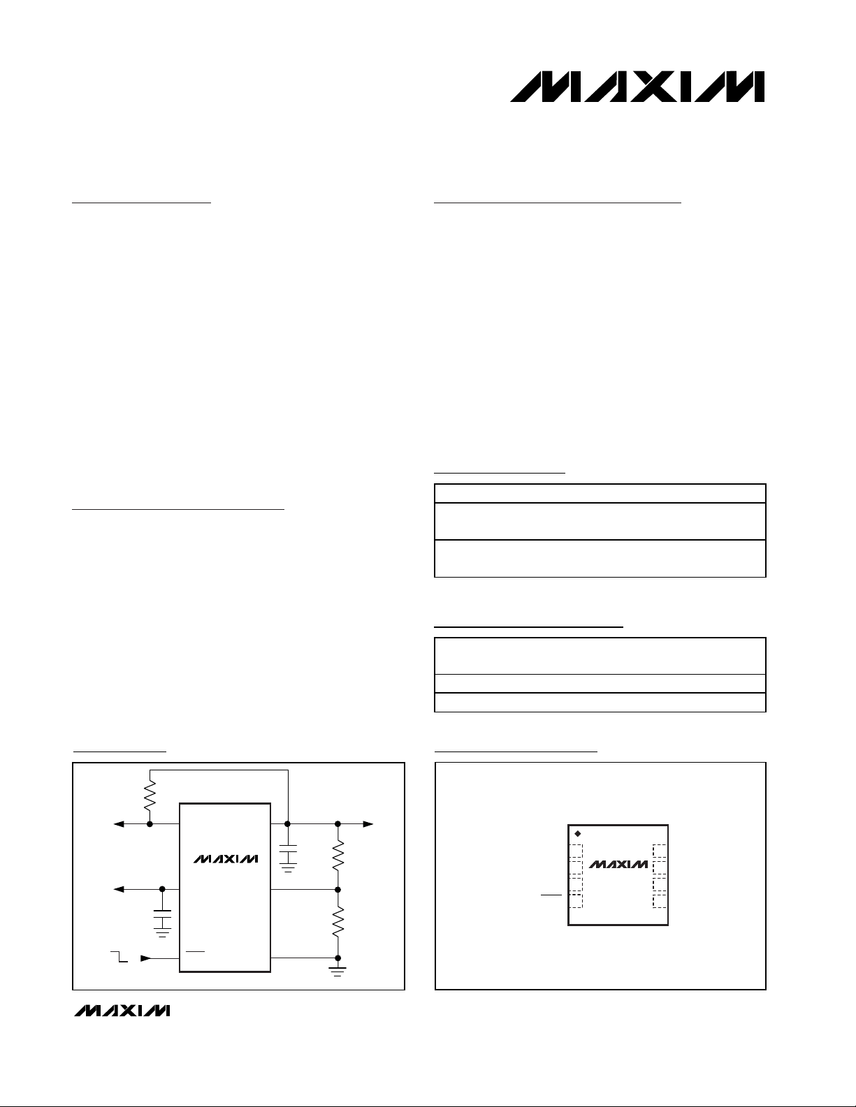
Pin Configuration
Ordering Information
OUT
SET
GND
IN
SHDN
POK
C
OUT
10µF
V
OUT
0.8V TO 4.5V
C
IN
1µF
ON
OFF
R
2
MAX1935
R
1
TO µC
R
POK
100kΩ
V
IN
2.25V TO 5.5V
Typical Operating Circuit
19-2599; Rev 0; 10/02
Selector Guide
For pricing, delivery, and ordering information, please contact Maxim/Dallas Direct! at
1-888-629-4642, or visit Maxim’s website at www.maxim-ic.com.
*Contact factory for preset output voltages.
PART T EM P R A N G E PIN-PACKAGE
MAX1935ETA* -40°C to +85°C
MAX1935ETA15* -40°C to +85°C
PART
MAX1935ETA Adjustable ADB
MAX1935ETA15 1.5V ADB
8 Thin QFN
3mm x 3mm
8 Thin QFN
3mm x 3mm
O U T PU T
VO L T A G E
TOP MARK
TOP VIEW
IN
IN
POK
OUT
1
2
MAX1935
3
4
THIN QFN
3mm x 3mm
8
OUT
7
SET
6
GNDSHDN
5

MAX1935
500mA, Low-Voltage Linear Regulator
in Tiny QFN
2 _______________________________________________________________________________________
ABSOLUTE MAXIMUM RATINGS
ELECTRICAL CHARACTERISTICS
(VIN= V
OUT(SETPOINT)
+ 500mV or VIN= 2.25V whichever is greater, SET = GND, SHDN = IN, TA= 0°C to +85°C, unless otherwise
noted. Typical values are at T
A
= +25°C.)
Stresses beyond those listed under “Absolute Maximum Ratings” may cause permanent damage to the device. These are stress ratings only, and functional
operation of the device at these or any other conditions beyond those indicated in the operational sections of the specifications is not implied. Exposure to
absolute maximum rating conditions for extended periods may affect device reliability.
IN, SHDN, POK, SET to GND ...................................-0.3V to +6V
OUT to GND ................................................-0.3V to (V
IN
+ 0.3V)
Output Short-Circuit Duration.....................................Continuous
Continuous Power Dissipation (T
A
= +70°C)
8-Pin Thin QFN (derate 24.4mW/°C above +70°C) .......1.95W
Operating Temperature .......................................-40°C to +85°C
Junction Temperature......................................................+150°C
Storage Temperature Range .............................-65°C to +150°C
Lead Temperature (soldering, 10s) .................................+300°C
Dual Mode is a trademark of Maxim Integrated Products, Inc.
PARAMETER SYMBOL CONDITIONS MIN TYP MAX UNITS
Input Voltage V
Input Undervoltage Lockout V
Output Voltage Accuracy
(Preset Mode)
Adjustable Output Voltage
SET Voltage Threshold
(Adjustable Mode)
Maximum Output Current I
Short-Circuit Current Limit I
SET Dual Mode™ Threshold 35 80 125 mV
SET Input Bias Current I
Ground-Pin Current I
Line Regulation ∆V
Load Regulation ∆V
Output Voltage Noise 10Hz to 1MHz, C
SHUTDOWN
Shutdown Supply Current I
S HDN Input Threshold
S HDN Input Bias Current I
Startup Time t
IN
UVLO
V
OUT
V
SET
OUT
LIM
SET
OFF
V
V
SHDN
STARTC OUT
Rising, 40mV hysteresis 1.85 2 2.15 V
TA = +25°C, I
TA = +25°C, I
OUT
OUT
TA = 0°C to +85°C, I
> V
OUT
+ 0.5V
OUT
OUT
V
IN
TA = +25°C, I
TA = +25°C, I
TA = 0°C to +85°C, I
V
> V
IN
V
OUT
V
SET
I
OUT
Q
I
OUT
OUT
LNRV I N
LDRIOUT
+ 0.5V
OUT
= 0V 600 1400 2300 mA
= 0.8V -100 +100 nA
= 1mA 210 600
= 500mA 575
= 500mA
fr om ( V
+ 100m V ) to 5.5V , I
OU T
= 1mA to 500mA 15.5 35 p p m /m A
S HDN = GND, VIN = 5.5V 0.02 5 µA
IH
IL
S HDN = GND or IN 10 100 nA
= 10µF, ti m e fr om S HDN hig h to P OK hig h40 µs
2.25 5.50 V
= 100mA -1.5 +1.5
= 1mA to 500mA -2.5 +2.5
= 1mA to 500mA,
OUT
-3 +3
0.8 4.5 V
= 100mA 788 812
= 1mA to 500mA 780 820
= 1mA to 500mA,
OUT
774 800 826
500 m A
V
= 2.25V 259 400
OUT
V
= 2.8V 201 350Dropout Voltage (Note 1) I
OUT
= 4V 147 275
V
OUT
= 5m A 0 0.125 %/V
L OA D
= 10µF (ESR < 0.1Ω) 300 µV
OUT
1.6
0.6
%
mV
RM S
µA
mV
RMS
V
MAX1935
500mA, Low-Voltage Linear Regulator
in Tiny QFN
_______________________________________________________________________________________ 3
ELECTRICAL CHARACTERISTICS (continued)
(VIN= V
OUT(SETPOINT)
+ 500mV or VIN= 2.25V whichever is greater, SET = GND, SHDN = IN, TA= 0°C to +85°C, unless otherwise
noted. Typical values are at T
A
= +25°C.)
ELECTRICAL CHARACTERISTICS
(VIN= V
OUT(SETPOINT)
+ 500mV or VIN= 2.25V whichever is greater, SET = GND, SHDN = IN, TA= -40°C to +85°C, unless otherwise
noted. Typical values are at T
A
= +25°C.) (Note 2)
PARAMETER SYMBOL CONDITIONS MIN TYP MAX UNITS
POWER-OK
POK Output Low Voltage V
Operating Voltage Range for
Valid POK Output
Output High Leakage Current V
Threshold Rising edge, referred to V
THERMAL PROTECTION
Ther m al- S hutd own Tem p erature T
Thermal-Shutdown Hysteresis ∆T
Sinking 2mA 5 50 mV
OL
Sinking 100µA 1.0 5.5 V
= 5.5V 100 nA
POK
OUT(NOMINAL)
SHDN
SHDN
90 93 96 %
170 °C
20 °C
PARAMETER SYMBOL CONDITIONS MIN TYP MAX UNITS
Input Voltage V
Input Undervoltage Lockout V
Output Voltage Accuracy
(Preset Mode)
Adjustable Output Voltage
SET Voltage Threshold
(Adjustable Mode)
Maximum Output Current I
Short-Circuit Current Limit I
SET Dual Mode Threshold 35 125 mV
SET Input Bias Current I
Ground-Pin Current I
SHUTDOWN
Shutdown Supply Current I
S HDN Input Threshold
S HDN Input Bias Current I
IN
UVLO
V
OUTIOUT
V
SETIOUT
OUT
LIM
SET
Q
OFF
V
IH
V
IL
SHDN
Rising, 40mV hysteresis 1.85 2.15 V
= 1mA to 500mA -4 +4 %
= 1mA to 500mA 766 834 mV
V
= 0V 600 2500 mA
OUT
V
= 0.8V -100 +100 nA
SET
I
= 1mA 400 µA
OUT
S HDN = GND, VIN = 5.5V 5 µA
2.5V < V
2.5V < V
S HDN = GND or IN 100 nA
< 5.5V 1.6
IN
< 5.5V 0.6
IN
2.25 5.50 V
0.8 4.5 V
500 m A
RM S
V
MAX1935
500mA, Low-Voltage Linear Regulator
in Tiny QFN
4 _______________________________________________________________________________________
ELECTRICAL CHARACTERISTICS (continued)
(VIN= V
OUT(SETPOINT)
+ 500mV or VIN= 2.25V whichever is greater, SET = GND, SHDN = IN, TA= -40°C to +85°C, unless otherwise
noted. Typical values are at T
A
= +25°C.) (Note 2)
Note 1: Dropout voltage is defined as VIN- V
OUT
, when V
OUT
is 100mV below the value of V
OUT
and when VIN= V
OUT(NOM)
+ 0.5V.
For 2.25V ≤ V
OUT
≤ 4V, dropout voltage limits are linearly interpolated from the values listed. For V
OUT
< 4V, dropout
voltage limit is equal to the value for V
OUT
= 4V.
Note 2: Specifications to -40°C are guaranteed by design, not production tested.
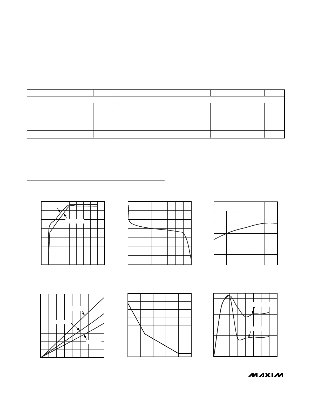
Typical Operating Characteristics
(V
OUT
= 3.3V, VIN= V
OUT
+ 500mV, SHDN = IN, CIN= 1µF, C
OUT
= 10µF, TA= +25°C, unless otherwise noted.)
0
1.0
0.5
2.0
1.5
3.0
2.5
3.5
1.5 2.5 3.02.0 3.5 4.0 4.5 5.0 5.5
OUTPUT VOLTAGE vs. INPUT VOLTAGE
MAX1935 toc01
INPUT VOLTAGE (V)
OUTPUT VOLTAGE (V)
I
OUT
= 0mA
I
OUT
= 500mA
6.0
3.25
3.26
3.28
3.27
3.30
3.31
3.29
3.32
0 200 300100 400 500 600 700 800
OUTPUT VOLTAGE vs. LOAD CURRENT
MAX1935 toc02
LOAD CURRENT (mA)
OUTPUT VOLTAGE (V)
3.28
3.30
3.29
3.32
3.31
3.33
3.34
-40 10-15 35 60 85
OUTPUT VOLTAGE vs. TEMPERATURE
MAX1935 toc03
TEMPERATURE (°C)
OUTPUT VOLTAGE (V)
VIN = V
OUT
+ 500mV
I
OUT
= 0
0
100
50
200
150
250
300
350
400
0 200 300100 400 500 600 700 800
DROPOUT VOLTAGE vs. LOAD CURRENT
MAX1935 toc04
LOAD CURRENT (mA)
DROPOUT VOLTAGE (mV)
TA = +85°C
TA = +25°C
TA = -40°C
0.14
0.16
0.18
0.20
0.22
0.24
0.26
0.28
2.0 2.5 3.0 3.5 4.0 4.5
DROPOUT VOLTAGE
vs. OUTPUT VOLTAGE
MAX1935 toc05
OUTPUT VOLTAGE (V)
DROPOUT VOLTAGE (V)
0
100
50
150
200
250
300
350
400
450
500
550
600
2.0 3.0 4.0 5.0 6.0
GROUND-PIN CURRENT
vs. INPUT VOLTAGE
MAX1935 toc06
INPUT VOLTAGE (V)
GROUND-PIN CURRENT (µA)
3.52.5 4.5 5.5
I
OUT
= 0mA
I
OUT
= 500mA
PARAMETER SYMBOL CONDITIONS MIN TYP MAX UNITS
POWER-OK
POK Output Low Voltage V
Operating Voltage Range for
Valid POK Output
Output High Leakage Current V
Threshold Rising edge, referred to V
Sinking 2mA 50 mV
OL
Sinking 100µA 1.0 5.5 V
= 5.5V 100 nA
POK
OUT(NOMINAL)
89 97 %

MAX1935
500mA, Low-Voltage Linear Regulator
in Tiny QFN
_______________________________________________________________________________________ 5
Typical Operating Characteristics (continued)
(V
OUT
= 3.3V, VIN= V
OUT
+ 500mV, SHDN = IN, CIN= 1µF, C
OUT
= 10µF, TA= +25°C, unless otherwise noted.)
100
200
150
300
250
350
400
450
500
0 200 300100 400 500 600 700 800
GROUND-PIN CURRENT
vs. LOAD CURRENT
MAX1935 toc07
LOAD CURRENT (mA)
GROUND-PIN CURRENT (µA)
VIN = 5.5V
VIN = 3.8V
150
160
180
170
190
200
-40 10-15 35 60 85
GROUND-PIN CURRENT
vs. TEMPERATURE
MAX1935 toc08
TEMPERATURE (°C)
GROUND-PIN CURRENT (µA)
VIN = V
OUT
+ 500mV
I
OUT
= 0
-60
0.01 0.1 1 10 100 1000
-50
-40
-30
-20
-10
0
POWER-SUPPLY REJECTION RATIO
vs. FREQUENCY
MAX1935 toc09
FREQUENCY (kHz)
PSRR (dB)
C
OUT
= 10µF
I
OUT
= 50mA
10
0.001
0.1 1 100 1000
OUTPUT SPECTRAL NOISE DENSITY
vs. FREQUENCY
0.01
0.1
1
MAX1935 toc10
FREQUENCY (kHz)
OUTPUT SPECTRAL NOISE DENSITY (µV/√Hz)
10
C
OUT
= 10µF
I
OUT
= 50mA
OUTPUT NOISE DC TO 1MHz
MAX1935 toc11
20ms/div
V
OUT
1mV/div
V
OUT
= 3.3V
R
OUT
= 66Ω (50mA)
0.01
0 200100 400 600 800700
REGION OF STABLE C
OUT
ESR
vs. LOAD CURRENT
0.1
1
10
100
MAX1935 toc12
FREQUENCY (kHz)
REGION OF C
OUT
ESR
300 500
C
OUT
= 10µF
STABLE REGION
LOAD-TRANSIENT RESPONSE
MAX1935 toc13
10µs/div
I
OUT
200mA/div
V
OUT
20mV/div
VIN = V
OUT
+ 500mV
C
IN
= 10µF
R
OUT
= 660Ω TO 6.6Ω (5mA TO 500mA)

MAX1935
500mA, Low-Voltage Linear Regulator
in Tiny QFN
6 _______________________________________________________________________________________
Pin Description
Typical Operating Characteristics (continued)
(V
OUT
= 3.3V, VIN= V
OUT
+ 500mV, SHDN = IN, CIN= 1µF, C
OUT
= 10µF, TA= +25°C, unless otherwise noted.)
LOAD-TRANSIENT RESPONSE
NEAR DROPOUT
MAX1935 toc14
10µs/div
I
OUT
200mA/div
V
OUT
50mV/div
VIN = V
OUT
+ 100mV
C
IN
= 10µF
R
OUT
= 660Ω TO
6.6Ω (5mA TO 500mA)
POK WAVEFORM
MAX1935 toc17
200µs/div
V
IN
2V/div
V
OUT
2V/div
5V
0
0
0
V
POK
2V/div
R
OUT
= 66Ω (50mA)
LINE-TRANSIENT RESPONSE
200µs/div
MAX1935 toc15
6V
VIN
1V/div
3V
V
OUT
10mV/div
SHUTDOWN WAVEFORM
R
= 6.6Ω (500mA)
OUT
20µs/div
MAX1935 toc16
2V
V
SHDN
1V/div
0
3V
V
OUT
1V/div
0
PIN NAME FUNCTION
1, 2 IN
3 POK
4 SHDN
5 GND
6 SET
7, 8 OUT
Regulator Input. Supply voltage can range from 2.25V to 5.5V. Bypass with a 1µF capacitor to GND (see
the Capacitor Selection and Regulation Stability section). Connect both input pins together externally.
Open-Drain, Active-Low Power-OK Output. POK remains low while the output voltage (V
POK threshold. Connect a 100kΩ pullup resistor from POK to OUT.
Active-Low Shutdown Input. A logic low at SHDN reduces supply current to 0.02µA. In shutdown, the POK
output is low. Connect SHDN to IN for normal operation.
Ground. This pin and the exposed pad also function as a heatsink. Solder both to a large pad or to the
circuit-board ground plane to maximize power dissipation.
Voltage-Setting Input. Connect SET to GND for preset output. Connect an external resistive voltage-divider
from OUT to SET to set the output voltage between 0.8V and 4.5V. The SET regulation voltage is 800mV.
Regulator Output. OUT sources up to 500mA. Bypass OUT with a 10µF low-ESR capacitor to GND.
Connect both OUT pins together externally.
) is below the
OUT

MAX1935
500mA, Low-Voltage Linear Regulator
in Tiny QFN
_______________________________________________________________________________________ 7
Detailed Description
The MAX1935 is a low-dropout, low-quiescent-current
linear regulator. The device supplies loads up to
500mA and is available with preset output voltages. As
illustrated in Figure 1, the MAX1935 includes a 0.8V reference, error amplifier, P-channel pass transistor, and
internal feedback voltage-divider.
The reference is connected to the error amplifier, which
compares it with the feedback voltage and amplifies
the difference. If the feedback voltage is lower than the
reference voltage, the pass-transistor gate is pulled
lower, which allows more current to pass to the output
increasing the output voltage. If the feedback voltage is
too high, the pass-transistor gate is pulled up, allowing
less current to pass to the output.
The output voltage is fed back through either an internal
resistive voltage-divider connected to OUT or an
external resistor network connected to SET. The dualmode comparator examines V
SET
and selects the feed-
back path. If V
SET
is below 35mV, the internal feedback
path is used, and the output is regulated to the factorypreset voltage. Additional blocks include an output
current limiter, thermal sensor, and shutdown logic.
Internal P-Channel Pass Transistor
The MAX1935 features a 0.4Ω P-channel MOSFET pass
transistor. Unlike similar designs using PNP pass
transistors, P-channel MOSFETs require no base drive,
which reduces operating current. PNP-based regulators
also waste considerable current in dropout when the
pass transistor saturates, and use high base-drive
currents under large loads. The MAX1935 does not
suffer from these problems.
Output Voltage Selection
The MAX1935’s dual-mode operation allows operation
in either a preset voltage mode or an adjustable mode.
Connect SET to GND to select the preset output
voltage. The two-digit part number suffix identifies the
output voltage. For example, the MAX1935ETA33 has a
preset 3.3V output voltage. The output voltage can also
be adjusted by connecting a voltage-divider from OUT
to SET (Figure 2). Select R2 in the 25kΩ to 100kΩ
range. Calculate R1 with the following equation:
R1 = R2 [(V
OUT
/ V
SET
) - 1]
where V
SET
= 0.8V, and V
OUT
can range from 0.8V
to 4.5V.
Shutdown
Drive SHDN low to enter shutdown. During shutdown,
the output is disconnected from the input, and supply
current drops to 0.02µA. When in shutdown, POK pulls
low. The capacitance and load at OUT determine the
rate at which V
OUT
decays. SHDN can be pulled as
high as 6V, regardless of the input and output voltage.
Power-OK Output
The POK output pulls low when OUT is less than 93% of
the nominal regulation voltage. Once OUT exceeds
93% of the nominal voltage, POK goes high impedance. POK is an open-drain N-channel output. To
obtain a logic voltage output, connect a pullup resistor
from POK to OUT. A 100kΩ resistor works well for most
applications. POK can be used to signal a microcontroller (µC), or drive an external LED to indicate power
failure. When the MAX1935 is shutdown, POK is held
low independent of the output voltage. If unused, leave
POK grounded or unconnected.
Current Limit
The MAX1935 monitors and controls the pass transistor’s gate voltage, limiting the output current to 1.4A
(typ). The output can be shorted to ground for an indefinite period of time without damaging the part.
Thermal-Overload Protection
Thermal-overload protection limits total power dissipation in the MAX1935. When the junction temperature
exceeds TJ= +170°C, a thermal sensor turns off the
pass transistor, allowing the device to cool. The thermal
sensor turns the pass transistor on again after the junction temperature cools by +20°C, resulting in a pulsed
output during continuous thermal-overload conditions.
Thermal-overload protection protects the MAX1935 in
the event of fault conditions. For continuous operation,
do not exceed the absolute maximum junction-temperature rating of TJ= +150°C.
Operating Region and Power Dissipation
The MAX1935’s maximum power dissipation depends
on the thermal resistance of the IC package and circuit
board, the temperature difference between the die
junction and ambient air, and the rate of air flow. The
power dissipated in the device is P = I
OUT
✕
(VIN-
V
OUT
). The maximum allowed power dissipation is
1.95W or:
PMAX = (T
J(MAX)
- TA) / (θJC+ θCA)
where TJ- TAis the temperature difference between the
MAX1935 die junction and the surrounding air, θ
JC
is
the thermal resistance from the junction to the case, and
θCAis the thermal resistance from the case through the
PC board, copper traces, and other materials to the surrounding air. The MAX1935 package features an
exposed thermal pad on its underside. This pad lowers
the package’s thermal resistance by providing

MAX1935
500mA, Low-Voltage Linear Regulator
in Tiny QFN
8 _______________________________________________________________________________________
a direct heat conduction path from the die to the PC
board. Connect the exposed backside pad and GND to
the system ground using a large pad or ground plane,
or multiple vias to the ground plane layer.
The MAX1935 delivers up to 0.5A(RMS) and operates
with input voltages up to 5.5V, but not simultaneously.
High output currents can only be sustained when inputoutput differential is within the limits outlined.
Applications Information
Capacitor Selection and Regulator
Stability
Connect a 1µF capacitor between IN and ground and a
10µF low equivalent series-resistance (ESR) capacitor
between OUT and ground. The input capacitor (CIN)
lowers the source impedance of the input supply.
Reduce noise and improve load-transient response,
stability, and power-supply rejection by using larger
output capacitors. The output capacitor’s (C
OUT
) ESR
affects stability and output noise. Use output capacitors
with an ESR of 0.1Ω or less to ensure stability and optimum transient response. Surface-mount ceramic
capacitors have very low ESR and are commonly available in values up to 10µF. Connect CINand C
OUT
as
close to the MAX1935 as possible.
Noise, PSRR, and Transient Response
The MAX1935 is designed to operate with low dropout
voltages and low quiescent currents, while still
maintaining good noise, transient response, and AC
rejection. See the Typical Operating Characteristics for
a plot of Power-Supply Rejection Ratio (PSRR) vs.
Frequency. When operating from noisy sources,
improved supply-noise rejection and transient response
can be achieved by increasing the values of the input
and output bypass capacitors and through passivefiltering techniques. The MAX1935 load-transient
Figure 1. Functional Diagram
V
IN
2.25V TO 5.5V
C
IN
1µF
IN
IN
MOSFET
DRIVER WITH
I
LIM
THERMAL
SENSOR
ON
OFF
LOGIC SUPPLY
VOLTAGE (V
OUT
)
R
POK
100kΩ
SHDN
SHUTDOWN
LOGIC
MAX1935
ERROR
AMPLIFIER
V
0.8V
REF
OUT
OUT
PRESET MODE
V
OUT
0.8V TO 3.3V
C
OUT
10µF
TO
µC
POK
93% V
REF
SET
80mV
GND

MAX1935
500mA, Low-Voltage Linear Regulator
in Tiny QFN
_______________________________________________________________________________________ 9
response graphs (see the Typical Operating
Characteristics) show two components of the output
response: a DC shift from the output impedance due to
the load current change, and the transient response. A
typical transient overshoot for a step change in the load
current from 5mA to 500mA is 40mV. Increasing the
output capacitor’s value and decreasing the ESR
attenuates the overshoot.
Input-Output (Dropout) Voltage
A regulator’s minimum input-to-output voltage differential
(dropout voltage) determines the lowest usable supply
voltage. In battery-powered systems, this determines the
useful end-of-life battery voltage. Because the MAX1806
uses a P-channel MOSFET pass transistor, its dropout
voltage is a function of drain-to-source on-resistance
(R
DS(ON)
) multiplied by the load current (see the Typical
Operating Characteristics):
V
DROPOUT
= VIN- V
OUT
= R
DS(ON)
✕
I
OUT
Chip Information
TRANSISTOR COUNT: 949
Figure 2. Adjustable Output Using External Feedback Resistors
Figure 3. Power Operating Regions: Maximum Output Current
vs. Input-Output Voltage Difference
V
0.8V
R
R
2
OUT
1
- 1
V
OUT
R1 = R2
V
IN
+2.25V TO +5.5V
C
IN
1µF
ON
OFF
IN
IN
MAX1935
SHDN
POK
OUT
OUT
SET
GND
C
OUT
10µF
600
500
400
300
200
MAXIMUM OUTPUT CURRENT (A)
100
0
0 5.0
INPUT-OUTPUT VOLTAGE DIFFERENCE (V)
TA = +70°C
TA = +85°C
4.54.03.53.02.52.01.51.00.5

MAX1935
500mA, Low-Voltage Linear Regulator
in Tiny QFN
Maxim cannot assume responsibility for use of any circuitry other than circuitry entirely embodied in a Maxim product. No circuit patent licenses are
implied. Maxim reserves the right to change the circuitry and specifications without notice at any time.
10 ____________________Maxim Integrated Products, 120 San Gabriel Drive, Sunnyvale, CA 94086 408-737-7600
© 2002 Maxim Integrated Products Printed USA is a registered trademark of Maxim Integrated Products.
Package Information
(The package drawing(s) in this data sheet may not reflect the most current specifications. For the latest package outline information,
go to www.maxim-ic.com/packages.)
COMMON DIMENSIONS
MIN. MAX.
SYMBOL
A
0.70 0.80
2.90 3.10
D
E
2.90 3.10
A1
0.00 0.05
L
0.20 0.40
k
0.25 MIN
A2 0.20 REF.
PACKAGE OUTLINE, 6, 8 & 10L,
QFN THIN (DUAL), EXPOSED PAD, 3x3x0.80 mm
21-0137
C
6, 8, &10L, QFN THIN.EPS
PACKAGE VARIATIONS
PKG. CODE
T633-1 1.50–0.10D22.30–0.10
N
6
1.50–0.10
E2
2.30–0.10T833-1 8
0.95 BSCeMO229 / WEEA
0.65 BSC
JEDEC SPEC
MO229 / WEEC
[(N/2)-1] x e
0.40–0.05b1.90 REF
1.95 REF0.30–0.05
0.25–0.05 2.00 REFMO229 / WEED-30.50 BSC1.50–0.10 2.30–0.1010T1033-1
PACKAGE OUTLINE, 6, 8 & 10L,
QFN THIN (DUAL), EXPOSED PAD, 3x3x0.80 mm
21-0137
C

 Loading...