

General Description
The MAX1932 generates a low-noise, high-voltage output
to bias avalanche photodiodes (APDs) in optical
receivers. Very low output ripple and noise is achieved by
a constant-frequency, pulse-width modulated (PWM)
boost topology combined with a unique architecture that
maintains regulation with an optional RC or LC post filter
inside its feedback loop. A precision reference and error
amplifier maintain 0.5% output voltage accuracy.
The MAX1932 protects expensive APDs against adverse
operating conditions while providing optimal bias.
Traditional boost converters measure switch current for
protection, whereas the MAX1932 integrates accurate
high-side current limiting to protect APDs under
avalanche conditions. A current-limit flag allows easy calibration of the APD operating point by indicating the precise point of avalanche breakdown. The MAX1932 control
scheme prevents output overshoot and undershoot to
provide safe APD operation without data loss.
The output voltage can be accurately set with either
external resistors, an internal 8-bit DAC, an external
DAC, or other voltage source. Output span and offset
are independently settable with external resistors. This
optimizes the utilization of DAC resolution for applications that may require limited output voltage range, such
as 4.5V to 15V, 4.5V to 45V, 20V to 60V, or 40V to 90V.
Applications
Optical Receivers and Modules
Fiber Optic Network Equipment
Telecom Equipment
Laser Range Finders
PIN Diode Bias Supply
Features
♦ Small Circuit Footprint
♦ Circuit Height < 2mm
♦ 2.7V to 5.5V Input
♦ 4.5V to 90V Output
♦ No Overshoot
♦ Accurate High-Side Current Limit
♦ Avalanche Indicator Flag
♦ 8-Bit SPI-Compatible DAC
♦ Compatible with External DAC
♦ 0.5% Accurate Output
♦ Low Ripple Output (< 1mV)
♦ Small 12-Pin, 4mm ✕ 4mm Thin QFN Package
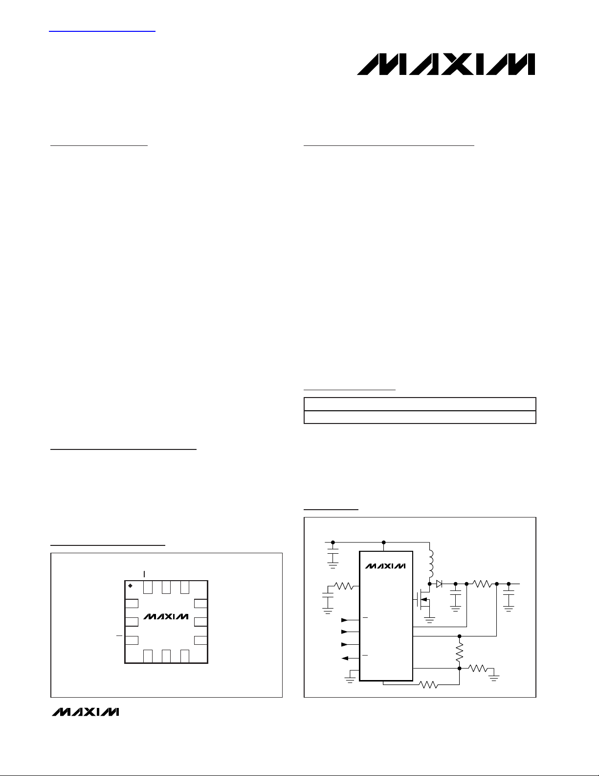
MAX1932
Digitally Controlled, 0.5% Accurate, Safest APD
Bias Supply
________________________________________________________________ Maxim Integrated Products 1
Ordering Information
19-2555; Rev 1; 12/02
For pricing, delivery, and ordering information, please contact Maxim/Dallas Direct! at
1-888-629-4642, or visit Maxim’s website at www.maxim-ic.com.
PART
TEMP RANGE
PIN-PACKAGE
MAX1932ETC
12 Thin QFN
MAX1932
INPUT
2.7V TO 5.5V
APD BIAS OUTPUT
4.5V TO 90V
DAC INPUTS
AVALANCHE
INDICATOR
FLAG
VIN
COMP
SCLK
GND
FB
CS-
CS+
GATE
DACOUT
DIN
CS
CL
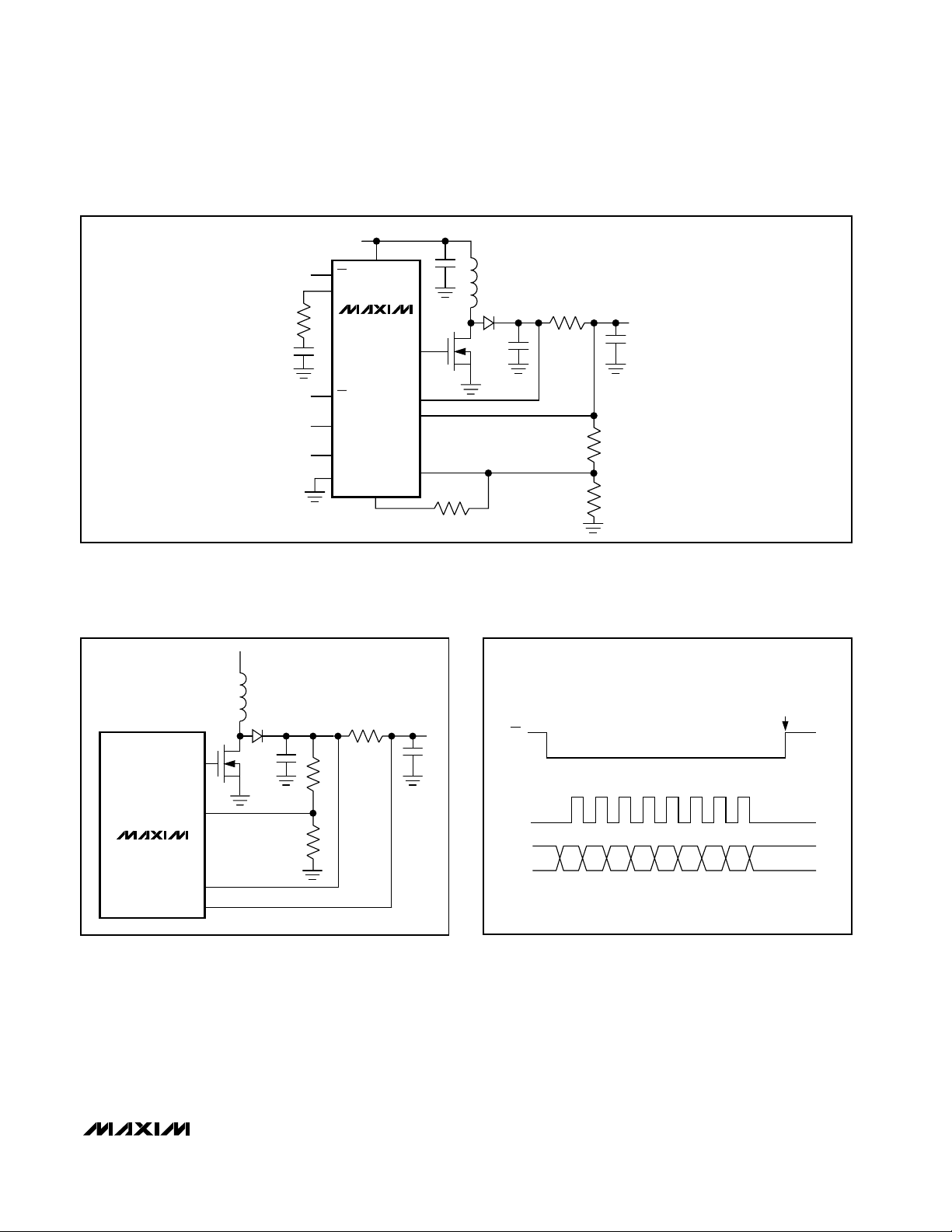
Typical Application Circuit
MAX1932
12
1
2
3
9
8
7
11 10
4 5 6
SCLK GND
COMP
FB
CS+
CS-
DACOUT GATE
VIN
DIN
CL
CS
Pin Configuration
查询MAX1932供应商
-40°C to +85°C
MAX1932
Digitally Controlled, 0.5% Accurate, Safest APD
Bias Supply
2 _______________________________________________________________________________________
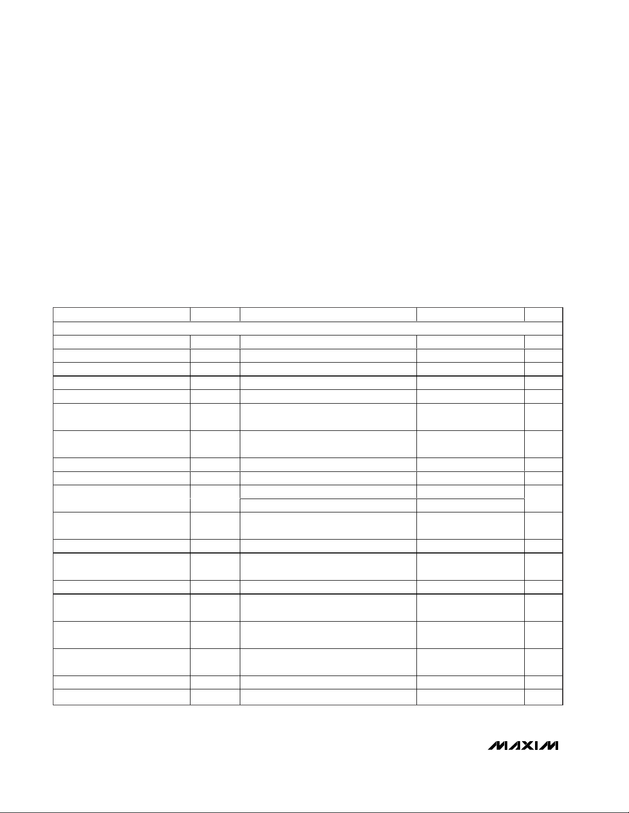
ABSOLUTE MAXIMUM RATINGS
ELECTRICAL CHARACTERISTICS
(VIN= 3.3V, CS = SCLK = DIN= 3.3V, CS+ = CS- = 45V, Circuit of Figure 2, TA= 0°C to +85°C, unless otherwise noted.)
Stresses beyond those listed under “Absolute Maximum Ratings” may cause permanent damage to the device. These are stress ratings only, and functional
operation of the device at these or any other conditions beyond those indicated in the operational sections of the specifications is not implied. Exposure to
absolute maximum rating conditions for extended periods may affect device reliability.
VIN to GND...............................................................-0.3V to +6V
DIN, SCLK, CS, FB to GND ......................................-0.3V to +6V
COMP, DACOUT, GATE, CL to GND ...........-0.3V to (V
IN
+0.3V)
CS+, CS- to GND .................................................-0.3V to +110V
Continuous Power Dissipation (T
A
= +70°C)
12-Pin Thin QFN (derate 16.9mW/°C above +70°C) .1349mW
Operating Temperature Range ...........................-40°C to +85°C
Junction Temperature......................................................+150°C
Storage Temperature Range .............................-65°C to +150°C
Lead Temperature (soldering 10s) ..................................+300°C
PARAMETER
SYMBOL
CONDITIONS
MIN
TYP
MAX
UNITS
GENERAL
Input Supply Range V
IN
2.7 5.5 V
VIN Undervoltage Lockout UVLO Both rise/fall, hysteresis = 100mV 2.1 2.6 V
Operating Supply Current I
IN
0.5 1 mA
VIN Shutdown Supply Current I
SHDN
00 hex loaded to DAC 25 65 µA
Input Resistance for CS+/CS- Resistance from either pin to ground 0.5 1 2.0 MΩ
Current-Limit Threshold
for CS+/CS-
V
Common-Mode Rejection
of Current Threshold
CS+ = 3V to 100V
%/V
Gate-Driver Resistance Gate high or low, I
GATE
= ±50mA 5 10 Ω
FB Input Bias Current -25
nA
TA = +25°C
FB Voltage V
FB
TA = 0°C to +85°C
V
FB Voltage
Temperature Coefficient
TCV
FB
%/°C
FB to COMP Transconductance COMP = 1.5V 50
200 µS
COMP Pulldown Resistance
in Shutdown
DAC code = 00 hex 100 Ω
D AC OU T to FB V ol tag e D i ffer ence
DAC code = FF hex -3 +3 mV
D AC OU T Differential Nonlinearity
(Note 1)
DAC Code = 01 to FF hex,
DAC guaranteed monotonic
-1 +1 LSB
D AC OU T Voltage Temperature
Coefficient
%/°C
DACOUT Load Regulation
DAC code = 0F to FF hex, source or sink
50µA
-1 +1 mV
Switching Frequency f
OSC
340 kHz
GATE Maximum On-Time t
ON
3µs
TCV
DACOUT
1.80 2.00 2.20
±0.005
1.24375 1.2500 1.25625
1.24250 1.2500 1.25750
0.0007
110
0.0007
250 300
+25
MAX1932
Digitally Controlled, 0.5% Accurate, Safest APD
Bias Supply
_______________________________________________________________________________________ 3
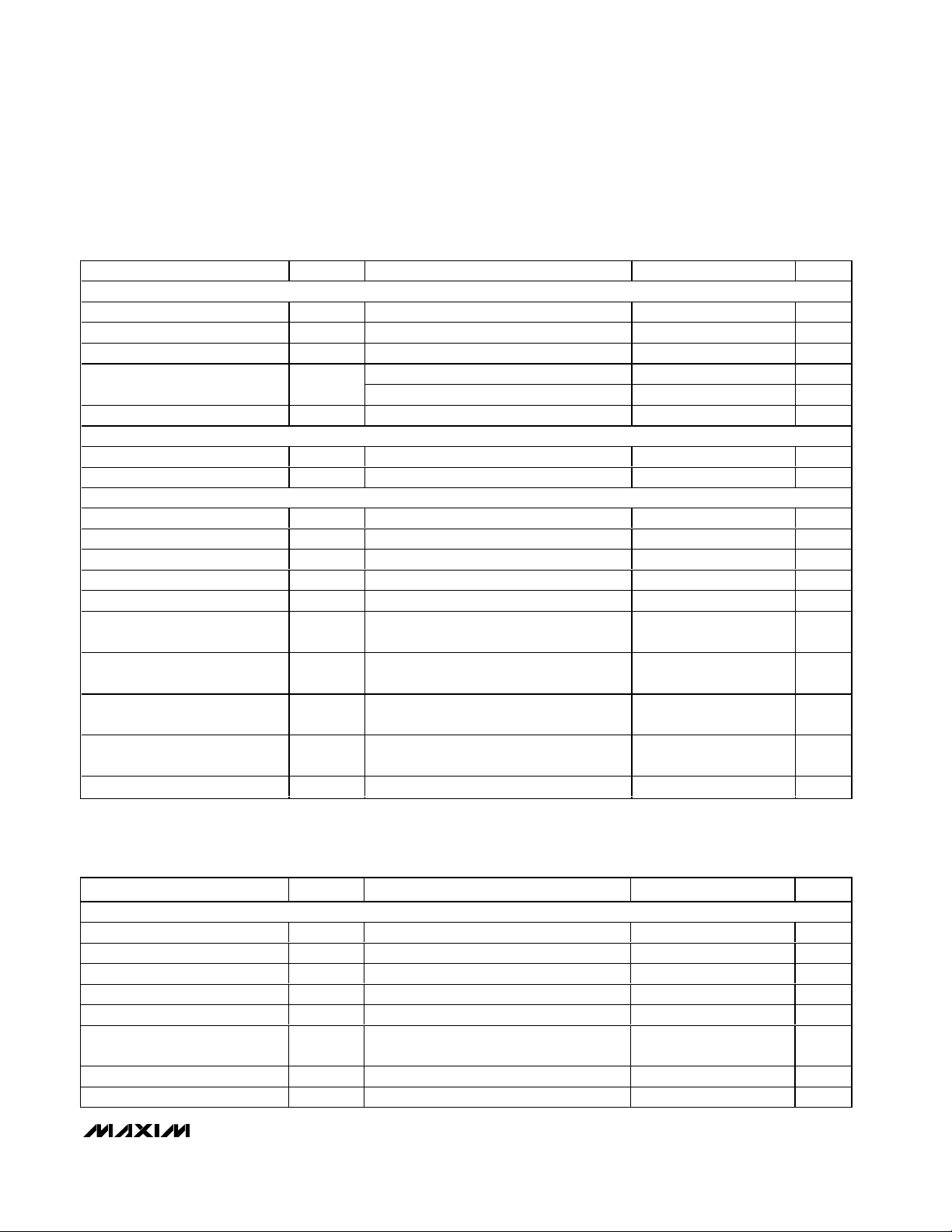
ELECTRICAL CHARACTERISTICS (continued)
(VIN= 3.3V, CS = SCLK = DIN= 3.3V, CS+ = CS- = 45V, Circuit of Figure 2, TA= 0°C to +85°C, unless otherwise noted.)
PARAMETER
SYMBOL
CONDITIONS
MIN
TYP
MAX
UNITS
DIGITAL INPUTS (DIN, SCLK, CS)
Input Low Voltage 0.6 V
Input High Voltage 1.4 V
Input Hysteresis
mV
TA = +25°C-1+1µA
Input Leakage Current
T
A
= 0°C to +85°C10nA
Input Capacitance 5pF
DIGITAL OUTPUT (CL)
Output Low Voltage I
SINK
= 1mA 0.1 V
Output High Voltage I
SOURCE
= 0.5mA V
IN
- 0.5 V
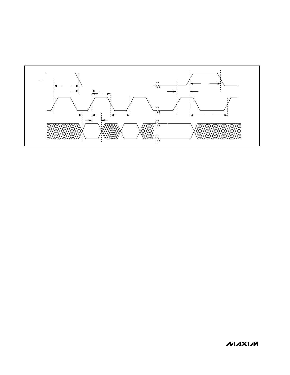
SPI TIMING (FIGURE 5)
SCLK Clock Frequency f
SCLK
2
MHz
SCLK Low Period t
CL
ns
SCLK High Period t
CH
ns
Data Hold Time t
DH
0ns
Data Setup Time t
DS
ns
CS Assertion to SCLK
Rising Edge Setup Time
t
CSS0
ns
CS Deassertion to SCLK
Rising Edge Setup Time
t
CSS1
ns
SCLK Rising Edge
to CS Deassertion
t
CSH1
ns
SCLK Rising Edge
to CS Assertion
t
CSH0
ns
CS High Period t
CSW
ns
ELECTRICAL CHARACTERISTICS
(VIN= 3.3V, CS = SCLK = DIN= 3.3V, CS+ = CS- = 45V, Circuit of Figure 2, TA= -40°C to +85°C, unless otherwise noted.) (Note 2)
PARAMETER
CONDITIONS
UNITS
GENERAL
Input Supply Range V
IN
2.7 5.5 V
VIN Undervoltage Lockout UVLO Both rise/fall, hysteresis = 100mV 2.1 2.6 V
Operating Supply Current I
IN
1mA
VIN Shutdown Supply Current I
SHDN
00 hex loaded to DAC 65 µA
Input Resistance for CS+/CS- Resistance from either pin to ground 0.5 2 MΩ
Current-Limit Threshold
for CS+/CS-
V
Gate-Driver Resistance Gate high or low, I
GATE
= ±50mA 10 Ω
FB Input Bias Current -30
nA
200
125
125
125
200
200
SYMBOL
200
200
300
MIN TYP MAX
1.80 2.20
+30
MAX1932
Digitally Controlled, 0.5% Accurate, Safest APD
Bias Supply
4 _______________________________________________________________________________________
Note 1: DACOUT = DAC code x (1.25V/256) + 1.25V/256.
Note 2: Specifications to -40°C are guaranteed by design and not production tested.
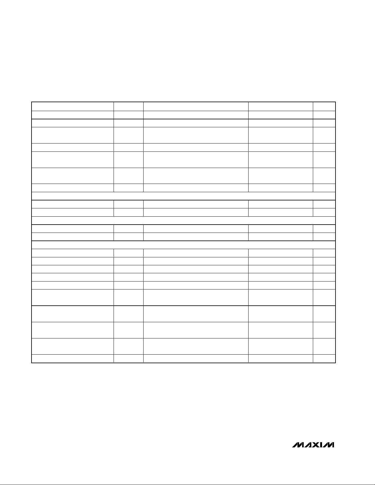
ELECTRICAL CHARACTERISTICS (continued)
(VIN= 3.3V, CS = SCLK = DIN= 3.3V, CS+ = CS- = 45V, Circuit of Figure 2, TA= -40°C to +85°C, unless otherwise noted.) (Note 2)
PARAMETER
CONDITIONS
UNITS
FB Voltage V
FB
V
FB to COMP Transconductance COMP = 1.5V 50 200 µS
COMP Pulldown Resistance
in Shutdown
DAC code = 00 hex 100 Ω
DAC code = FF hex -4 +4 mV
D AC OU T Differential Nonlinearity
(Note 1)
DAC Code = 01 to FF hex, DAC
guaranteed monotonic
-1 +1 LSB
D AC OU T Load Regulation
DAC code = 0F to FF hex, source or sink
50µA
-1 +1 mV
Switching Frequency f
OSC
360 kHz
DIGITAL INPUTS (DIN, SCLK, CS)
Input Low Voltage 0.6 V
Input High Voltage 1.4 V
DIGITAL OUTPUT (CL)
Output Low Voltage I
SINK
= 1mA 0.1 V
Output High Voltage I
SOURCE
= 0.5mA
V
SPI TIMING (FIGURE 5)
SCLK Clock Frequency f
SCLK
2
MHz
SCLK Low Period t
CL
125 ns
SCLK High Period t
CH
125 ns
Data Hold Time t
DH
0ns
Data Setup Time t
DS
125 ns
CS Assertion to SCLK
Rising Edge Setup Time
t
CSS0
200 ns
CS Deassertion to SCLK
Rising Edge Setup Time
t
CSS1
200 ns
SCLK Rising Edge
to CS Deassertion
t
CSH1
200 ns
SCLK Rising Edge
to CS Assertion
t
CSH0
200 ns
CS High Period t
CSW
300 ns
SYMBOL
MIN TYP MAX
1.23875 1.26125
D AC OU T to FB V ol tag e D i ffer ence
240
V
- 0.5
IN
MAX1932
Digitally Controlled, 0.5% Accurate, Safest APD
Bias Supply
_______________________________________________________________________________________ 5
SWITCHING WAVEFORMS
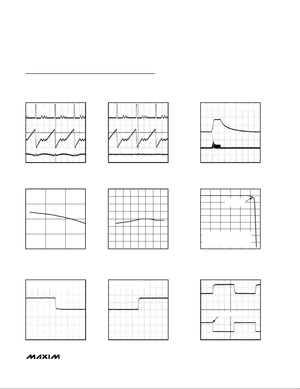
MAX1932 toc01
1µs/div
0.05A/div
50V/div
0.002V/div
V
LX
I
L
V
OUT
RIPPLE (AC-COUPLED)
V
OUT
= 90V
SWITCHING WAVEFORM WITH LC FILTER
MAX1932 toc02
1µs/div
0.05A/div
50V/div
0.002V/div
V
LX
I
L
V
OUT
RIPPLE (AC-COUPLED)
V
OUT
= 90V, L = 300µH, C = 1µF, FIGURE 7
STARTUP AND SHUTDOWN WAVEFORMS
MAX1932 toc03
20ms/div
50mA/div
50V/div
INPUT
CURRENT
OUTPUT
VOLTAGE
OUTPUT VOLTAGE vs. INPUT VOLTAGE
MAX1932 toc04
INPUT VOLTAGE (V)
OUTPUT VOLTAGE (V)
4.53.5
89
90
91
92
88
2.5 5.5
VFB vs. TEMPERATURE
MAX1932 toc05
TEMPERATURE (°C)
VFB (V)
8060-40 -20 0 20 40
1.2485
1.2490
1.2495
1.2500
1.2505
1.2510
1.2515
1.2520
1.2480
-60 100
OUTPUT VOLTAGE vs. LOAD CURRENT
MAX1932 toc06
LOAD CURRENT (mA)
OUTPUT VOLTAGE (V)
2.52.01.51.00.5
55
60
65
70
75
80
85
90
95
50
0 3.0
CURRENT LIMIT
ACTIVATED
VCC = 5V, INDUCTOR = 100µH,
R1 = 806Ω
FEEDBACK DIVIDER CURRENT AND CSCURRENT INCLUDED
OUTPUT VOLTAGE STEP-DOWN
DUE TO DAC CHANGE
MAX1932 toc07
10ms/div
1V/div
V
OUT
AT
64.233V
OFFSET = 62.962V = 88 hex
STEP DOWN FROM 80 hex TO 88 hex
OUTPUT VOLTAGE STEP-UP
DUE TO DAC CHANGE
MAX1932 toc08
10ms/div
1V/div
V
OUT
AT
62.692V
OFFSET
OFFSET = 62.962V = 88 hex
STEP VALUE = 64.233 = 80 hex
OUTPUT VOLTAGE STEP
DUE TO DACOUT CHANGE
MAX1932 toc09
20ms/div
20V/div
0.5V/div
DACOUT EXTERNAL SOURCE
Typical Operating Characteristics
(VIN= 5V, Circuit of Figure 2, TA=+25°C, unless otherwise noted)
MAX1932
Detailed Description
Fixed Frequency PWM
The MAX1932 uses a constant frequency, PWM, controller architecture. This controller sets the switch ontime and drives an external N-channel MOSFET (see
Figure 1). As the load varies, the error amplifier sets the
inductor peak current necessary to supply the load and
regulate the output voltage.
Output Current Limit
The MAX1932 uses an external resistor at CS+ and CSto sense the output current (see Figure 2). The typical
current-limit threshold is 2V. CL is designed to help find
the optimum APD bias point by going low to indicate
when the APD reaches avalanche and that current limit
has been activated. To minimize noise, CL only
changes state on an internal oscillator edge.
Output Control DAC
An internal digital-to-analog converter can be used to
control the output voltage of the DC-DC converter
(Figure 2). The DAC output is changed through an SPI™
serial interface using an 8-bit control byte. On power-up,
the DAC defaults to FF hex (1.25V), which corresponds
to a minimum boost converter output voltage.
Alternately, the output voltage can be set with external
resistors, an external DAC, or a voltage source. Output
span and offset are independently settable with exter-
nal resistors. See the Applications Information section
for output control equations.
SPI Interface/Shutdown
Use an SPI-compatible 3-wire serial interface with the
MAX1932 to control the DAC output voltage and to shut
down the MAX1932. Figures 4 and 5 show timing diagrams
for the SPI protocol. The MAX1932 is a write-only device
and uses CS along with SCLK and DIN to communicate.
The serial port is always operational when the device is
powered. To shut down the DC-DC converter portion only,
update the DAC registers to 00 hex.
Applications Information
Voltage Feedback Sense Point
Feedback can be taken from in front of, or after, the current-limit sense resistor. The current-limit sense resistor
forms a lowpass filter with the output capacitor. Taking
feedback after the current-limit sense resistor (see Figure
2), optimizes the output voltage accuracy, but requires
overcompensation, which slows down the control loop
response. For faster response, the feedback can be
taken from in front of the current-sense resistor (see
Figure 3). This configuration however, makes the output
voltage more sensitive to load variation and degrades
output accuracy by an amount equal to the load current
times the current-sense resistor value.
Digitally Controlled, 0.5% Accurate, Safest APD
Bias Supply
6 _______________________________________________________________________________________
Pin Description
PIN
FUNCTION
1 SCLK DAC Serial Clock Input
2 DIN DAC Serial Data Input
3 CL Current-Limit Indicator Flag. CL = 0 indicates that the part is in current limit. Logic high level = VIN.
4 CS+
Current-Limit Plus Sense Input. Connect a resistor from CS+ to CS- in series with the output. The differential
threshold is 2V. CS+ has typically 1MΩ resistance to ground.
5 CS- Current-Limit Minus Sense Input. CS- has typically 1MΩ resistance to ground.
6
Internal DAC Output. Generates a control voltage for adjustable output operation. DACOUT can source or
sink 50µA.
7FB
Feedback input. Connect to a resistive voltage-divider between the output voltage (V
OUT
) and FB to set the
output voltage. The feedback set point is 1.25V.
8
Compensation Pin. Compensates the DC-DC converter control loop with a series RC to GND. COMP is
actively discharged to ground during shutdown or undervoltage conditions.
9 GND Ground
10 GATE Gate-Driver Output for External N-FET
11 VIN IC Supply Voltage (2.7V to 5.5V). Bypass VIN with a 1µF or greater ceramic capacitor.
12 CS DAC Chip-Select Input
SPI is a trademark of Motorola, Inc.
NAME
DACOUT
COMP

Output and DAC Adjustments Range
Many biasing applications require an adjustable output
voltage, which is easily obtained using the MAX1932’s
DAC output (Figure 2).
The DAC output voltage is given by the following equation:
On power-up, DACOUT defaults to FF hex or 1.25V,
which corresponds to the minimum V
OUT
output voltage.
The voltage generated at DACOUT is coupled to FB
through R6. DACOUT can sink only 50µA so:
Select the minimum output voltage (V
OUTFF
), and the
maximum output voltage (V
OUT01
) for the desired
adjustment range. R5 sets the adjustment span using
the following equation:
R5 = (V
OUTFF
- V
OUT01
) (R6/1.25V)
R8 sets the minimum output of the adjustment range
with the following equation:
R8 = (1.25V ✕ R5)/(V
OUTFF
)
Setting the Output Voltage without
the DAC
Adjust the output voltage by connecting a voltagedivider from the output (V
OUT
) to FB (Figure 2 with R6
omitted). Select R8 between 10kΩ to 50kΩ. Calculate
R5 with the following equation:
Inductor Selection
Optimum inductor selection depends on input voltage,
output voltage, maximum output current, switching frequency, and inductor size. Inductors are typically specified by their inductance (L), peak current (IPK), and
resistance (LR).
The inductance value is given by:
where V
IN
is the input voltage, I
OUT(MAX)
is the maxi-
mum output current delivered, V
OUT
is the output volt-
age, and T is the switching period (3.3µs), η is the
estimated power conversion efficiency, and D is the
maximum duty cycle:
D < (V
OUT
- VIN)/V
OUT
up to a maximum of 0.9
Since the L equation factors in efficiency, for inductor calculation purposes, an η of 0.5 to 0.75 is usually suitable.
For example, with a maximum DC load current of 2.5mA,
a 90V output, VIN= 5V, D = 0.9, T = 3.3µs, and η esti-
mated at 0.75, the above equation yields an L of 111µH,
so 100µH would be a suitable value.
The peak inductor current is given by:
These are typical calculations. For worst case, refer to
the article titled “Choosing the MAX1932 External
Indicator, Diode, Current Sense Resistor, and Output
Filter Capacitor for Worst Case Conditions” located on
the Maxim website in the Application Notes section (visit
www.maxim-ic.com/an1805).
External Power-Transistor Selection
An N-FET power switch is required for the MAX1932. The
N-FET switch should be selected to have adequate onresistance with the MOSFET VGS= V
IN(MIN)
. The break-
down voltage of the N-FET must be greater than V
OUT
.
For higher-current output applications (such as 5mA at
90V), SOT23 high-voltage low-gate-threshold N-FETs
may not have adequate current capability. For example,
with a 5V input, a 90V, 5mA output requires an inductor
peak of 240mA. For such cases it may be necessary to
simply parallel two N-FETs to achieve the required current rating. With SOT23 devices this often results in
smaller and lower cost than using a larger N-FET device.
Diode Selection
The output diode should be rated to handle the output
voltage and the peak switch current. Make sure that the
diode’s peak current rating is at least IPKand that its
breakdown voltage exceeds V
OUT
. Fast reverse recov-
ery time (trr< 10ns) and low junction capacitance
I
VDT
L
PK
IN
=
××
L
VDT
IV
IN
OUT MAX OUT
=
()
×××
×
2
2
2
η
()
RR
VOUT
V
58
125
1=−
.
R
V
A
6
125
50≥µ
.
V CODE
VV
DACOUT
=×
+
125
256
125
256
..
MAX1932
Digitally Controlled, 0.5% Accurate, Safest APD
Bias Supply
_______________________________________________________________________________________ 7

MAX1932
(<10pF) are recommended to minimize losses. A smallsignal silicon switching diode is suitable if efficiency is
not critical.
Output Filter Capacitor Selection
The output capacitors of the MAX1932 must have high
enough voltage rating to operate with the V
OUT
required. Output capacitor effective series resistance
(ESR) determines the amplitude of the high-frequency
ripple seen on the output voltage. In the typical application circuit, a second RC formed by R1 and C3 further
reduces ripple.
Input Bypass Capacitor Selection
The input bypass capacitor reduces the peak currents
drawn from the voltage source and reduces noise
caused by the MAX1932’s switching action. The input
source impedance determines the size of the capacitor
required at the input (VIN). A low ESR capacitor is recommended. A 1µF ceramic capacitor is adequate for
most applications. Place the bypass capacitor as close
as possible to the VIN and GND pins.
Current-Sense Resistor Selection
Current limit is used to set the maximum delivered output current. In the typical application circuit, MAX1932
is designed to current limit at:
Note that I
LIMIT
must include current drawn by the feedback divider (if sensing feedback after R1) and the
input current of CS-.
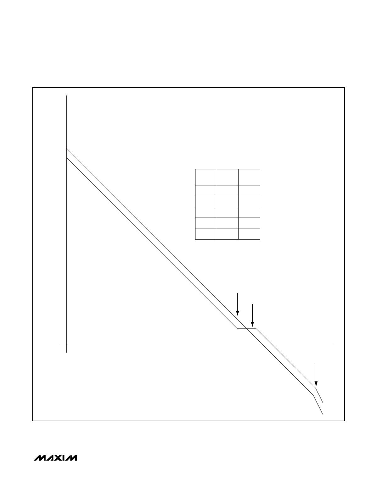
Stability and Compensation
Component Selection
Compensation components, R7 and C4, introduce a
pole and a zero necessary to stabilize the MAX1932
(see Figure 6). The dominant pole, POLE1, is formed by
the output impedance of the error amplifier (REA) and
C4. The R7/C4 zero, ZERO1, is selected to cancel the
pole formed by the output filter cap C3 and output load
RLD, POLE2. The additional pole of R1/C3, POLE3,
should be at least a decade past the crossover frequency to not affect stability:
POLE1 (dominant pole) = 1 / (2π ✕ R
EA
✕ C4)
ZERO1 (integrator zero) = 1 / (2π ✕ R7 ✕ C4)
POLE2 (output load pole) = K1 / (2π ✕ R
LD
✕ (C2 + C3))
POLE3 (output filter pole) = 1 / (2π ✕ R1 ✕ C3)
The DC open-loop gain is given by:
AOL= K2 ✕ Gm ✕ R
EA
where REA= 310MΩ,
gM= 110µS,
RLDis the parallel combination of feedback network
and the load resistance.
A properly compensated MAX1932 results in a gain vs.
frequency plot that crosses 0dB with a single pole
slope (20dB per decade). See Figure 6.
Table 1 lists suggested component values for several
typical applications.
Further Noise Reduction
The current-limit sense resistor is typically used as part
of an output lowpass filter to reduce noise and ripple.
For further reduction of noise, an LC filter can be added
as shown in Figure 7. Output ripple and noise with and
without the LC filter are shown in the Typical Operating
Characteristics. If a post LC filter is used, it is best to
use a coil with fairly large resistance (or a series resistor) so that ringing at the response peak of the LC filter
is damped. For a 330µH and 1µF filter, 22Ω accom-
plishes this, but a resistor is not needed if the coil resistance is greater than 15Ω.
Output Accuracy and Feedback
Resistor Selection
The MAX1932 features 0.5% feedback accuracy. The
total voltage accuracy of a complete APD bias circuit is
the sum of the FB set-point accuracy, plus resistor ratio
error and temperature coefficient. If absolute accuracy
is critical, the best resistor choice is an integrated network with specified ratio tolerance and temperature
coefficient. If using discrete resistors in high-accuracy
applications, pay close attention to resistor tolerance
and temperature coefficients.
Temperature Compensation
APDs exhibit a change in gain as a function of temperature. This gain change can be compensated with an
appropriate adjustment in bias voltage. For this reason
it may be desirable to vary the MAX1932 output voltage
as a function of temperature. This can be done in soft-
K
V Volts
Volts
V
VV
V
VV
R T ond
L Henries
FB IN
OUT IN
OUT
OUT IN
LD
2
075
2
2
2
=×
×
×
×
×
×
()
.( )
()
()
-
-
sec
K
VV
VV
OUT IN
OUT IN
12=
× -
-
R
V
I
LIMIT
12=
Digitally Controlled, 0.5% Accurate, Safest APD
Bias Supply
8 _______________________________________________________________________________________

ware by the system through the on-chip DAC, but can
also be accomplished in hardware using an external
thermistor or IC temperature sensor. Figure 8 shows
how an NTC thermistor can be connected to make the
bias voltage increase with temperature.
PC Board Layout and Grounding
Careful PC board layout is important for minimizing
ground bounce and noise. In addition, keep all connections to FB as a short as possible. In particular, locate
feedback resistors (R5, R6, and R8) as close to FB as
possible. Use wide, short traces to interconnect large
current paths for N1, D1, L1, C1, C2. Do not share
these connections with other signal paths. Refer to the
MAX1932 EV kit for a PC board layout example.
Chip Information
TRANSISTOR COUNT: 1592
PROCESS: BICMOS
MAX1932
Digitally Controlled, 0.5% Accurate, Safest APD
Bias Supply
_______________________________________________________________________________________ 9
VIN, V
OUT
, I
OUT(MAX)
INDUCTOR L1
(µH)
C
SNS
C2 (µF)
R
SNS
R1 (Ω)
C
OUT
C3 (µF)
R
COMP
R7 (kΩ)
C
COMP
C4 (µF)
5VIN, 40-90V
OUT
at 2.5mA 100 0.047 806 0.1 20 0.22
5VIN, 20-60V
OUT
at 2.5mA 150 0.10 806 0.047 15 0.22
5VIN, 20-60V
OUT
at 5mA 82 0.22 392 0.10 10 0.47
3VIN, 40-90V
OUT
at 2.5mA 33 0.047 806 0.1 20 0.22
3VIN, 4.5-15V
OUT
at 2.5mA
220 0.47 806 0.01 7.5 0.47
Table 1. Compensation Components for Typical Circuits (Figure 2)

MAX1932
Digitally Controlled, 0.5% Accurate, Safest APD
Bias Supply
10 ______________________________________________________________________________________
987kΩ
987kΩ
13kΩ
COMP
ERROR
COMPARATOR
CS+
CS-
PWM CONTROL
AND GATE DRIVER
GATE
SPI
SERIAL
INTERFACE
SCLK
REF
1.25V
UVLO
FB
ERROR
AMPLIFIER
8-BIT DAC
DIN
8
REF
DACOUT
CLIM
BUFFER
VIN
GND
CL
13kΩ
CS
RAMP
OSC
Figure 1. Functional Diagram
MAX1932
Digitally Controlled, 0.5% Accurate, Safest APD
Bias Supply
______________________________________________________________________________________ 11
MAX1932
INPUT
2.7V TO 5.5V
VOUT
40V TO 90V
VIN
COMP
SCLK
GND
FB
CS-
CS+
GATE
DACOUT
DIN
CS
CL
R7
20kΩ
C4
0.22µF
C1 1µF
R1
806Ω
N1
BSS123
L1
100µH
D1
100V
C2
0.047
C3
0.1µF
R5
1MΩ
R8
32.4kΩ
R6
24.9kΩ
Figure 2. Typical Operating Circuit
DIN
SCLK
18
D7 D6
D5
D4 D3
D2
D1 DO
CS
INSTRUCTION
EXECUTED
Figure 4. Serial Interface Timing Diagram
MAX1932
VOUT
FB
CS-
CS+
GATE
Figure 3. Taking Feedback Ahead of Output Filter
MAX1932
Digitally Controlled, 0.5% Accurate, Safest APD
Bias Supply
12 ______________________________________________________________________________________
CS
SCLK
DIN
t
DS
t
DH
t
CL
t
CH
t
CSS0
t
CSH0
t
CSW
t
CSH1
t
CSS1
Figure 5. Detailed Serial Interface Timing Diagram
MAX1932
Digitally Controlled, 0.5% Accurate, Safest APD
Bias Supply
______________________________________________________________________________________ 13
20
FREQUENCY (Hz)
0.01 0.1 1.0
36Hz
100 1k 10k
40
60
80
100
120
POLE1
ZERO1
POLE2
POLE3
A
OL
0.0023Hz
36Hz
36Hz
4.2kHz
102dB
0.0023Hz
36Hz
91Hz
4.2kHz
98dB
90V,
1mA
90V,
2.5mA
MAGNITUDE (dB)
91Hz
4.2k
10
Figure 6. Loop Response

MAX1932
Digitally Controlled, 0.5% Accurate, Safest APD
Bias Supply
14 ______________________________________________________________________________________
MAX1932
VOUT
330µH
0.1µF1µF
FB
CS-
CS+
GATE
VIN
Figure 7. Adding a Post LC Filter
MAX1932
VIN
VOUT
TO CS+ TO CS-
FB
GATE
R1
R5
R8
R9
R10
NTC
THERMISTOR
Figure 8. Adding an NTC Thermistor for Hardware Temperature Compensation; Output Voltage Increases with Temperature Rise

MAX1932
Digitally Controlled, 0.5% Accurate, Safest APD
Bias Supply
______________________________________________________________________________________ 15
Package Information
(The package drawing(s) in this data sheet may not reflect the most current specifications. For the latest package outline information,
go to www.maxim-ic.com/packages.)
21-0139 A
PACKAGE OUTLINE
12,16,20,24L QFN THIN, 4x4x0.8 mm

MAX1932
Digitally Controlled, 0.5% Accurate, Safest APD
Bias Supply
Maxim cannot assume responsibility for use of any circuitry other than circuitry entirely embodied in a Maxim product. No circuit patent licenses are
implied. Maxim reserves the right to change the circuitry and specifications without notice at any time.
16 ____________________Maxim Integrated Products, 120 San Gabriel Drive, Sunnyvale, CA 94086 408-737-7600
© 2002 Maxim Integrated Products Printed USA is a registered trademark of Maxim Integrated Products.
Package Information (continued)
(The package drawing(s) in this data sheet may not reflect the most current specifications. For the latest package outline information,
go to www.maxim-ic.com/packages.)
A21-0139
PACKAGE OUTLINE
12,16,20,24L QFN THIN, 4x4x0.8 mm

Copyright © Each Manufacturing Company.
All Datasheets cannot be modified without permission.
This datasheet has been download from :
www.AllDataSheet.com
100% Free DataSheet Search Site.
Free Download.
No Register.
Fast Search System.
www.AllDataSheet.com
 Loading...