

Page 1
General Description
The MAX1931 is a current-limited, 60mΩ switch with
built-in fault blanking. Its accurate preset current limit of
0.64A to 1.06A makes it ideally suited for USB applications. The device’s low quiescent supply current (14µA)
and shutdown current (1µA) conserve battery power in
portable applications. The MAX1931 operates with
inputs from 2.7V to 5.5V, making it ideal for both 3V and
5V systems.
A fault signal notifies the microprocessor that the internal current limit has been reached. A 10ms fault-blanking feature allows momentary faults (such as those
caused when hot-swapping into a capacitive load) to be
ignored, thus preventing false alarms to the host system.
This fault blanking also prevents a fault signal from
being issued when the device is powering up.
In the MAX1931, an output overcurrent condition causes
the switch to current limit at 0.64A to 1.06A and FAULT
to go low after the 10ms blanking period. When the
overcurrent condition is removed, FAULT returns to its
high-impedance state.
The MAX1931 has several safety features to ensure that
the USB port is protected. Built-in thermal overload
protection limits power dissipation and junction temperatures. The device has an accurate internal current-limiting circuitry to protect the input supply against overload.
The MAX1931 is available in a space-saving 10-pin
µMAX package.
Applications
USB Ports and Hubs
Notebook Computers
Portable Equipment
Docking Stations
Hot Plug-In Power Supplies
Battery-Charger Circuits
Features
♦ 0.5A Guaranteed Output Current
♦ Guaranteed 0.75A Short-Circuit Protection
♦ 10ms Internal Fault-Blanking Timeout
♦ No Fault Signal During Power-Up
♦ Thermal Shutdown Protection
♦ 2.7V to 5.5V Supply Range
♦ 14µA Supply Current
♦ Small 10-Pin µMAX Package
MAX1931
Current-Limited Switch for Single USB Port
_______________________________________________________________ Maxim Integrated Products 1
Typical Operating Circuit
19-2357; Rev 0; 4/02
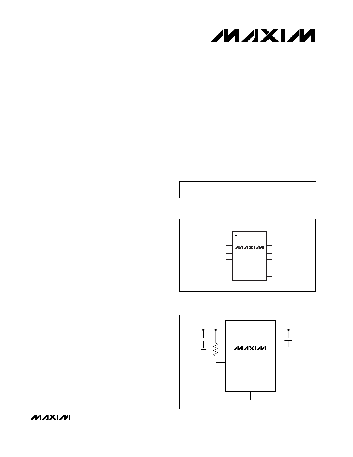
Pin Configuration
For pricing, delivery, and ordering information, please contact Maxim/Dallas Direct! at
1-888-629-4642, or visit Maxim’s website at www.maxim-ic.com.
Ordering Information
PART TEMP RANGE PIN-PACKAGE
MAX1931EUB -40°C to +85°C 10µMAX
TOP VIEW
OUT
1
IN
2
MAX1931
3
IN
4
5
MAX
µ
10
OUT
9
IN
8
OUT
7
FAULTOUT
GNDON
6
INPUT
2.7V TO 5.5V
IN
OUT
OUTPUT
MAX1931
FAULT
OFF
ON
ON
GND
Page 2
MAX1931
Current-Limited Switch for Single USB Port
2 _______________________________________________________________________________________
ABSOLUTE MAXIMUM RATINGS
ELECTRICAL CHARACTERISTICS
(VIN= 5V, TA= 0°C to +85°C, unless otherwise noted. Typical values are at TA= +25°C.)
Stresses beyond those listed under “Absolute Maximum Ratings” may cause permanent damage to the device. These are stress ratings only, and functional
operation of the device at these or any other conditions beyond those indicated in the operational sections of the specifications is not implied. Exposure to
absolute maximum rating conditions for extended periods may affect device reliability.
IN, ON (ON), FAULT to GND....................................-0.3V to +6V
OUT to GND ................................................-0.3V to (V
IN
+ 0.3V)
Maximum Continuous Switch Current .....1.2A (internally limited)
OUT Short Circuit to GND ..........................................Continuous
Continuous Power Dissipation (T
A
= +70°C)
10-Pin µMAX (derate 5.6mW/°C above +70°C) ............444mW
Operating Temperature Range ............................-40°C to +85°C
Storage Temperature Range .............................-65°C to +150°C
Lead Temperature (soldering, 10s) .................................+300°C
VON= GND, I
OUT
= 0
I
SINK
= 1mA, VIN= 3V
VON= VINor GND
V
OUT
= 4.5V
VIN= 2.7V to 3.6V
VIN= 2.7V to 5.5V
TA= +25°C
VON= VIN= V
OUT
= 5.5V
Rising edge, 100mV hysteresis
VON= V
IN
V
IN
= 5.5V,
V
OUT
= GND
OUT shorted to GND
CONDITIONS
V0.4V
OL
FAULT Output Logic
Low Voltage
µA±1
ON Input Leakage
V
2
V
IH
ON Input Logic High Voltage
V0.8V
IL
ON Input Logic Low Voltage
mA500 700I
SC
Continuous Short-Circuit
Current Limit
µA
35
I
Q
14 35
V2.7 5.5V
IN
Operating Voltage
Quiescent Current
mA640 850 1060I
LIMIT
Current Limit
mΩ
72 180
R
ON
On-Resistance
150
60 110
µA0.001 1Off Supply Current
V2.0 2.6UVLOUndervoltage Lockout
0.01 4
µA
20
Off Switch Leakage
UNITSMIN TYP MAXSYMBOLPARAMETER
Timer not running
Timer running
TA= +25°C
TA= 0°C to +85°C
VIN= 4.4V to 5.5V
VIN= 4.4V to 5.5V
VIN= 3V
VIN= V
FAULT
= 5.5V µA1
FAULT Output High
Leakage Current
From overcurrent condition to FAULT assertion
ms61013t
FB
Fault-Blanking Timeout Period
VIN= 5V, C
OUT
= 150µF, RL= 15Ω,
from ON driven low to 50% full V
OUT
ms1Startup Time
I
LOAD
= 400mA µs3620t
OFF
Switch Turn-Off Time
I
LOAD
= 400mA µs80 200t
ON
Switch Turn-On Time
°C165Thermal Shutdown Threshold
TA= 0°C to +85°C
VIN= 3.7V to 5.5V 2.4
Page 3
MAX1931
Current-Limited Switch for Single USB Port
_______________________________________________________________________________________ 3
ELECTRICAL CHARACTERISTICS
(VIN= 5V, TA= -40°C to +85°C, unless otherwise noted.) (Note 1)
VIN= V
FAULT
= 5.5V µA1
VIN= 4.4V to 5.5V
FAULT Output High
Leakage Current
VON= GND, I
OUT
= 0, timer not running
From overcurrent condition to FAULT assertion
I
SINK
= 1mA, VIN= 3V
VON= VINor GND
V
OUT
= 4.5V
VIN= 3V to 3.6V
VIN= 3V to 5.5V
ms
VON= VIN= V
OUT
= 5.5V
Rising edge, 100mV hysteresis
VIN= 3V
VON= V
IN
= 5.5V, V
OUT
= GND
OUT shorted to GND
CONDITIONS
614t
FB
Fault-Blanking Timeout Period
I
LOAD
= 400mA µs120t
OFF
Switch Turn-Off Time
I
LOAD
= 400mA µs200t
ON
Switch Turn-On Time
V0.4V
OL
FAULT Output Logic
Low Voltage
µA±1
ON Input Leakage
V
2
V
IH
ON Input Logic High Voltage
V0.8V
IL
ON Input Logic Low Voltage
mA750
Continuous Short-Circuit
Current Limit
µAI
Q
35
V3 5.5V
IN
Operating Voltage
Quiescent Current
mA600 1100I
LIMIT
Current Limit
180
150
µA2Off Supply Current
V2.0 2.9UVLOUndervoltage Lockout
µA20Off Switch Leakage
UNITSMIN TYP MAXSYMBOLPARAMETER
R
ON
On-Resistance mΩ
Note 1: Specifications to -40°C are guaranteed by design, not production tested.
VIN= 3.7V to 5.5V 2.4
Page 4

MAX1931
Current-Limited Switch for Single USB Port
4 _______________________________________________________________________________________
Typical Operating Characteristics
(VIN= 5V, TA= +25°C, unless otherwise noted.)
0
2
4
6
8
10
12
14
16
021 3456
QUIESCENT CURRENT vs. INPUT VOLTAGE
MAX1931 toc01
INPUT VOLTAGE (V)
QUIESCENT CURRENT (µA)
I
OUT
= O
V
ON (ON)
= GND (VIN)
9
11
10
13
12
15
14
16
-40 0 20-20 40 60 80 100
QUIESCENT CURRENT vs. TEMPERATURE
MAX1931 toc02
TEMPERATURE (°C)
QUIESCENT CURRENT (µA)
VIN = 5V
VIN = 3V
100
0.01
OFF SUPPLY CURRENT
vs. TEMPERATURE
0.1
1
10
MAX1931 toc03
TEMPERATURE (°C)
OFF SUPPLY CURRENT (nA)
-40 0-20 20406080100
VON (ON) = V
IN
(GND)
100
1000
0.01
-40 0-20 40 10080
OFF SWITCH CURRENT vs. TEMPERATURE
0.1
1
10
MAX1931 toc04
TEMPERATURE (°C)
OFF SWITCH CURRENT (nA)
20 60
V0N
(ON)
= V
IN
(GND)
-40 0-20 40 10080
NORMALIZED ON-RESISTANCE
vs. TEMPERATURE
MAX1931 toc05
TEMPERATURE (°C)
NORMALIZED R
ON
20 60
0
0.4
0.2
0.8
0.6
1.2
1.0
1.4
I
OUT
= 425mA
0
0.4
0.2
0.8
0.6
1.0
1.2
0231 456
NORMALIZED OUTPUT CURRENT
vs. OUTPUT VOLTAGE
MAX1931 toc06
OUTPUT VOLTAGE (V)
NORMALIZED OUTPUT CURRENT
SHORT-CIRCUIT CURRENT
I
LIMIT
0
40
20
80
60
140
120
100
160
-40 0-20 20 40 60 80 100
TURN-ON TIME vs. TEMPERATURE
MAX1931 toc07
TEMPERATURE (°C)
t
ON
(µs)
I
LOAD
= 425mA
VIN = 3V
VIN = 5V
0
2
1
4
3
6
5
7
-40 0 20-20 40 60 80 100
TURN-OFF TIME vs. TEMPERATURE
MAX1931 toc08
TEMPERATURE (°C)
t
OFF
(µs)
I
LOAD
= 425mA
VIN = 3V
VIN = 5V
Page 5

MAX1931
Current-Limited Switch for Single USB Port
_______________________________________________________________________________________ 5
Typical Operating Characteristics (continued)
(VIN= 5V, TA= +25°C, unless otherwise noted.)
4
3
1
2
2ms/div
MAX1931 toc10
CURRENT-LIMIT AND FAULT RESPONSE
CH1 = VIN, 200mV/div, AC-COUPLED; CH2 = V
OUT
,
5V/div; CH3 = V
FAULT
, 5V/div; CH4 = I
OUT
, 500mA/div
4
10µs/div
3
1
2
CURRENT-LIMIT RESPONSE
MAX1931 toc11
CH1 = VIN, 200mV/div, AC-COUPLED; CH2 = V
OUT
,
5V/div; CH3 = V
FAULT
, 5V/div; CH4 = I
OUT
, 1A/div
4
3
2
1
SWITCH TURN-ON TIME
MAX1931 toc12
CH1 = V
OUT
, 5V/div; CH2 = VON, 5V/div;
CH3 = V
FAULT
, 5V/div; CH4 = I
OUT
, 200mA/div
20µs/div
0
2
6
4
10
8
12
-40 0 20-20 40 60 80 100
FAULT-BLANKING TIMEOUT
vs. TEMPERATURE
MAX1931 toc09
TEMPERATURE (°C)
FAULT-BLANKING TIMEOUT (ms)
VIN = 3V OR 5V
I
OUT
= 850mA
4
3
2
1
SWITCH TURN-OFF TIME
MAX1931 toc13
CH1 = V
OUT
, 5V/div; CH2 = VON, 5V/div;
CH3 = V
FAULT
, 5V/div; CH4 = I
OUT
, 200mA/div
1µs/div
4
3
2
1
STARTUP TIME
(TYPICAL USB APPLICATION)
MAX1931 toc14
CH1 = V
OUT
, 5V/div; CH2 = VON, 5V/div;
CH3 = I
OUT
, 500mA/div; CH4 = V
FAULT
, 5V/div
1ms/div
CL = 150µF
R
L
= 15Ω
RESISTOR
LOAD
CURRENT
FULL CURRENT LIMIT CHARGES CAPACITOR
FOLDBACK
CURRENT LIMIT
Page 6
MAX1931
Current-Limited Switch for Single USB Port
6 _______________________________________________________________________________________
_______________Detailed Description
The MAX1931 P-channel MOSFET power switch limits
output current to 0.64A (min) to 1.06A (max). When the
output current is increased beyond the current limit
(I
LIMIT
), the current also increases through the replica
switch (I
OUT
/ 6500). The current-limit error amplifier
compares the voltage to the internal 1.24V reference
and regulates the current back to the I
LIMIT
.
This switch is not bidirectional; therefore, the input voltage must be higher than the output voltage.
Continuous Short-Circuit Protection
The MAX1931 is a foldback short-circuit-protected
switch. In the event of an output short-circuit or currentoverload condition, the current through the switch is
foldback-current-limited to 500mA continuous.
Thermal Shutdown
The MAX1931 features thermal shutdown. The switch
turns off and the FAULT output goes low immediately
(no fault blanking) when the junction temperature
exceeds +165°C. When the MAX1931 cools 20°C, the
switch turns back on. If the fault short-circuit condition
is not removed, the switch cycles on and off, resulting
in a pulsed output.
FAULT Indicator
The MAX1931 provides a fault output (FAULT). A
100kΩ pullup resistor from FAULT to IN provides a
logic control signal. This open-drain output goes low
when any of the following conditions occur:
• The input voltage is below the undervoltage lockout
(UVLO) threshold.
• The die temperature exceeds the thermal shutdown
temperature limit of +165°C.
• The device is in current limit and the 10ms faultblanking period is exceeded.
Fault Blanking
The MAX1931 features 10ms fault blanking. Fault
blanking allows current-limit faults, including momentary short-circuit faults that occur when hot-swapping a
capacitive load, and also ensures that no fault is issued
during power-up. When a load transient causes the
device to enter current limit, an internal counter starts. If
the load fault persists beyond the 10ms fault-blanking
timeout, the FAULT output asserts low. Ensure that the
MAX1931’s input is adequately bypassed to prevent
input glitches from triggering spurious FAULT outputs.
Input voltage glitches less than 150mV do not cause a
Pin Description
NAME FUNCTION
1, 3, 9 IN
Input. P-channel MOSFET source. Connect all IN pins together and bypass with a 1µF
ceramic capacitor to ground.
PIN
2, 4, 8, 10 OUT
Switch Output. P-channel MOSFET drain. Connect all OUT pins together and bypass with a
0.1µF capacitor to ground.
5
ON
Active-Low Switch On Input. A logic low turns the switch on.
6 GND Ground
7
FAULT
Fault-Indicator Output. This open-drain output goes low when the device is in thermal shutdown, undervoltage lockout, or on a sustained (>10ms) current-limit condition.
Figure 1. Functional Diagram
IN
FAULT
N
ON
P
P
OUT
MAX1931
REPLICA
AMPLIFIER
ON
P
10ms
TIMER
HOT
ON
CURRENT-LIMIT
AMPLIFIER
1.24V
GND
CONTROL
CIRCUITRY
Page 7

MAX1931
Current-Limited Switch for Single USB Port
_______________________________________________________________________________________ 7
spurious FAULT output. Load-transient faults less than
10ms (typ) do not cause a FAULT output assertion.
Only current-limit faults are blanked. Die overtemperature faults and input voltage droops below the UVLO
threshold cause an immediate fault output.
Applications Information
Input Capacitor
To limit the input voltage drop during momentary output
short-circuit conditions, connect a capacitor from IN to
GND. A 1µF ceramic capacitor is adequate for most
applications; however, higher capacitor values further
reduce the voltage drop at the input (see Figure 2).
Output Capacitor
Connect a 0.1µF capacitor from OUT to GND. This capacitor helps prevent inductive parasitics from pulling
OUT negative during turn-off.
Layout and Thermal Dissipation
To optimize the switch-response time to output shortcircuit conditions, it is very important to keep all traces
as short as possible to reduce the effect of undesirable
parasitic inductance. Place input and output capacitors
as close to the device as possible (no more than 5mm).
All IN and all OUT pins must be connected with short
traces to the power bus. Wide power bus planes provide superior heat dissipation through the switch IN and
OUT pins. Figure 3 shows suggested pin connections
for a single-layer board.
Under normal operating conditions, the package can
dissipate and channel heat away. Calculate the maximum power dissipation as follows:
P = (I
LIMIT
)
2
✕
R
ON
where I
LIMIT
is the preset current limit (1.1A max) and
RONis the on-resistance of the switch (150mΩ max).
When the output is short-circuited, foldback-current-limiting activates and the voltage drop across the switch
equals the input supply. The power dissipated across
the switch increases, as does the die temperature. If the
fault condition is not removed, the thermal-overload protection circuitry activates (see the Thermal Shutdown
section). Wide power-bus planes connected to IN and
OUT and a ground plane in contact with the device
help dissipate additional heat.
Figure 3. IN and OUT Cross Connections for a Single-Layer
Board
Figure 2. Typical Application Circuit
Chip Information
TRANSISTOR COUNT: 715
MAX1931
IN OUTPUTOUT
INPUT
2.7V TO 5.5V
FAULT
ON
ON
OFF
100kΩ
1µF 0.1µF*
*USB SPECIFICATIONS REQUIRE A LARGER CAPACITOR
GND
MAX1931
1
2
3
4
5
IN
OUT
IN
OUT
ON
OUT
IN
OUT
FAULT
GND
10
9
8
7
6
Page 8

MAX1931
Current-Limited Switch for Single USB Port
Maxim cannot assume responsibility for use of any circuitry other than circuitry entirely embodied in a Maxim product. No circuit patent licenses are
implied. Maxim reserves the right to change the circuitry and specifications without notice at any time.
Maxim Integrated Products, 120 San Gabriel Drive, Sunnyvale, CA 94086 408-737-7600 _____________________ 8
© 2002 Maxim Integrated Products Printed USA is a registered trademark of Maxim Integrated Products.
Note: MAX1931 does not have an exposed pad.
Package Information
(The package drawing(s) in this data sheet may not reflect the most current specifications. For the latest package outline information,
go to www.maxim-ic.com/packages.)
10LUMAX.EPS
 Loading...