

Page 1
MAX1922
1A Current-Limited Switch for 2 USB Ports
________________________________________________________________
Maxim Integrated Products
1
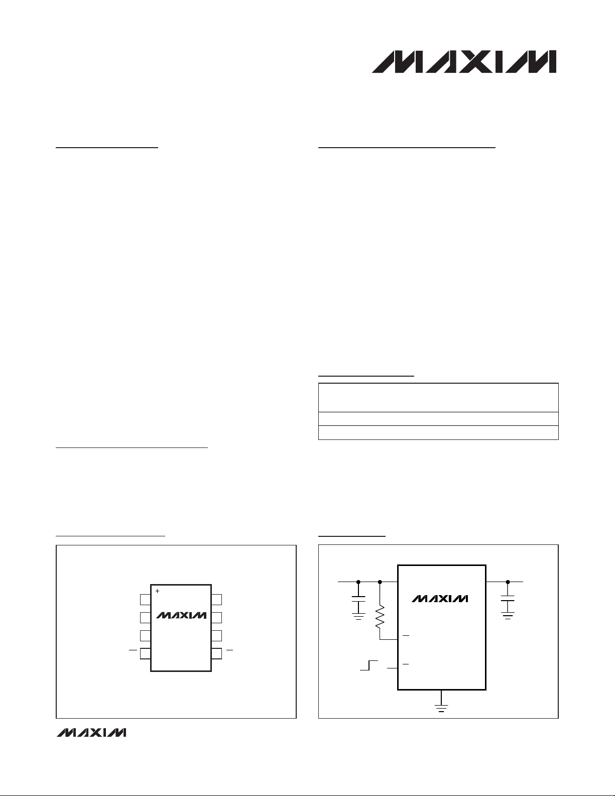
Typical Operating Circuit
19-2254; Rev 3; 4/09
Pin Configurations
Ordering Information
General Description
The MAX1922 current-limited 70mΩ switch with built-in
fault blanking provides an accurate, preset 1.4A to 2.1A
current limit, making it ideal for dual USB applications.
Its low quiescent supply current (16µA) and standby
current (1µA) conserve battery power in portable applications. The MAX1922 operates with inputs from 2.7V
to 5.5V, making it ideal for both 3V and 5V systems.
An overcurrent signal (OC) notifies the microprocessor
that the internal current limit has been reached. A 10ms
overcurrent-blanking feature allows momentary faults
(such as those caused when hot-swapping into a
capacitive load) to be ignored, thus preventing false
alarms to the host system. This blanking also prevents
an OC signal from being issued when the device is
powering up.
The MAX1922 has several safety features to ensure that
the USB port is protected. Built-in thermal-overload protection limits power dissipation and junction temperature. The device also has accurate internal currentlimiting circuitry to protect the input supply against
overload.
The MAX1922 is offered in a space-saving 8-pin SO
package and a 10-pin TDFN package and operates over
the extended (-40°C to +85°C) temperature range.
Applications
Notebook Computers
USB Ports
USB Hubs
Docking Stations
Features
o Accurate Current Limit (1.4A min, 2.1A max)
o 10ms Internal OC Blanking Timeout
o OC Blanking During Power-Up
o 125mΩ (max) High-Side MOSFET
o Short-Circuit and Thermal Protection with
Overcurrent Logic Output
o Undervoltage Lockout
o 16µA Quiescent Supply Current
o 1µA (max) Standby Supply Current
o 2.7V to 5.5V Supply Range
o UL Recognized: UL# E211395
For pricing, delivery, and ordering information, please contact Maxim Direct at 1-888-629-4642,
or visit Maxim’s website at www.maxim-ic.com.
*
EP = Exposed paddle.
+
Denotes a lead(Pb)-free/RoHS-compliant package.
Pin Configurations continued at end of data sheet.
PART TEMP RANGE
MAX1922ESA+ -40°C to +85°C 8 SO
MAX1922ETB+ -40°C to +85°C 10 TDFN-EP* AQQ
PINPACKAGE
MARK
TOP
—
TOP VIEW
1
GND
2
MAX1922
3
IN
EN
4
SO
87OUT
OUTIN
OUT
6
OC
5
INPUT
2.7V TO 5.5V
OFF
ON
IN OUTPUTOUT
MAX1922
OC
EN
GND
Page 2
MAX1922
1A Current-Limited Switch for 2 USB Ports
2 _______________________________________________________________________________________
ABSOLUTE MAXIMUM RATINGS
ELECTRICAL CHARACTERISTICS
(VIN= 5V, TA= 0°C to +85°C, unless otherwise noted. Typical values are at TA= +25°C.)
Stresses beyond those listed under “Absolute Maximum Ratings” may cause permanent damage to the device. These are stress ratings only, and functional
operation of the device at these or any other conditions beyond those indicated in the operational sections of the specifications is not implied. Exposure to
absolute maximum rating conditions for extended periods may affect device reliability.
IN, EN, OC to GND...................................................-0.3V to +6V
OUT to GND ................................................-0.3V to (V
IN
+ 0.3V)
Maximum Switch Current.........................2.3A (internally limited)
OUT Short-Circuit to GND ..........................................Continuous
Continuous Power Dissipation (T
A
= +70°C)
8-Pin SO (derate 5.88mW/°C above +70°C)................471mW
10-Pin TDFN (derate 18.5mW/°C above +70°C) .......1481mW
Operating Temperature Range (extended).........-40°C to +85°C
Storage Temperature Range .............................-65°C to +150°C
Lead Temperature (soldering, 10s) .................................+300°C
)
OPERATING CONDITION
Input Voltage V
POWER SWITCH
Switch Static Drain-Source OnState Resistance
Switch Turn-On Time t
Switch Turn-Off Time t
ENABLE INPUT (EN)
EN High-Level Input Voltage V
EN Low-Level Input Voltage V
EN Input Current VEN = VIN or GND -1 1 µA
Startup Time
CURRENT LIMIT
Overload Output Current I
Short-Circuit Output Current I
SUPPLY CURRENT
Supply Current, Low-Level Input VEN = VIN = V
Supply Current, High-Level
Input
Supply-Leakage Current
UNDERVOLTAGE LOCKOUT
Undervoltage Lockout UVLO Rising edge, 100mV hysteresis 2.0 2.4 2.6 V
OVERCURRENT (OC)
OC Threshold 1.1 A
OC Output Low Voltage V
PARAMETER SYMBOL CONDITIONS MIN TYP MAX UNITS
IN
TA = +25°C VIN = 4.4V to 5.5V 70 100
R
DS(ON
LIMIT
ON
OFF
IH
IL
SC
I
Q
OL
TA = 0°C to +85°C
I
= 400mA 80 200 µs
LOAD
I
= 400mA 3 6 20 µs
LOAD
VIN = 2.7V to 3.6V 2.0
VIN = 3.7V to 5.5V 2.4
VIN = 2.7V to 5.5V 0.8 V
V
= 5V, C
IN
to 50% full V
Force V
= 150µF from EN driven low
OUT
OUT
to 4.5V 1.4 1.75 2.1 A
OUT
OUT shorted to GND 1 1.4 A
OUT
VEN = 0, I
V
= VIN = 5.5V,
EN
V
= 0
OUT
I
= 1mA, VIN = 3V 0.4 V
SINK
OUT
= 0
VIN = 4.4V to 5.5V 125
V
= 3V 72 150
IN
= 5.5V 0.002 1 µA
Timer not running 16 25
Timer running 35
TA = +25°C 0.01 2
T
= 0°C to +85°C 15
A
2.7 5.5 V
1ms
mΩ
V
µA
µA
Page 3
MAX1922
1A Current-Limited Switch for 2 USB Ports
_______________________________________________________________________________________ 3
Note 1: Specifications to -40°C are guaranteed by design, not production tested.
ELECTRICAL CHARACTERISTICS
(VIN= 5V, TA= -40°C to +85°C, unless otherwise noted.) (Note 1)
ELECTRICAL CHARACTERISTICS (continued)
(VIN= 5V, TA= 0°C to +85°C, unless otherwise noted. Typical values are at TA= +25°C.)
)
OC Off-State Current VIN = VOC = 5V 1 µA
OC Blanking Timeout Period t
THERMAL SHUTDOWN
Thermal Shutdown Threshold 165 °C
PARAMETER SYMBOL CONDITIONS MIN TYP MAX UNITS
BL
From overcurrent condition to OC assertion 6 10 13 ms
PARAMETER SYMBOL CONDITIONS MIN TYP MAX UNITS
OPERATING CONDITION
Input Voltage V
POWER SWITCH
Switch Static Drain-Source
On-State Resistance
Switch Turn-On Time t
Switch Turn-Off Time t
ENABLE INPUT (EN)
EN High-Level Input Voltage V
EN Low-Level Input Voltage V
EN Input Current VEN = VIN or GND -1 1 µA
CURRENT LIMIT
Overload Output Current I
Short-Circuit Output Current I
SUPPLY CURRENT
Supply Current, Low-Level Input VEN = VIN = V
Supply Current, High-Level
Input
Supply Leakage Current VEN = VIN = 5.5V, V
UNDERVOLTAGE LOCKOUT
Undervoltage Lockout UVLO Rising edge, 100mV hysteresis 2.0 2.9 V
OVERCURRENT (OC)
OC Threshold 1.1 A
OC Output Low Voltage V
OC Off-State Current VIN = VOC = 5V 1 µA
OC Blanking Timeout Period t
R
DS(ON
LIMIT
IN
ON
OFF
IH
IL
SC
I
Q
OL
BL
VIN = 4.4V to 5.5V 125
VIN = 3V 150
I
= 400mA 200 µs
LOAD
I
= 400mA 1 20 µs
LOAD
VIN = 3.0V to 3.6V 2.0
VIN = 3.7V to 5.5V 2.4
VIN = 3.0V to 5.5V 0.8 V
Force V
OUT shorted to GND 1.5 A
VEN = GND, I
I
SINK
From overcurrent condition to OC assertion 6 14 ms
to 4.5V 1.2 2.3 A
OUT
= 5.5V 2 µA
OUT
= 0, timer not running 25 µA
OUT
= GND 15 µA
OUT
= 1mA, VIN = 3V 0.4 V
3.0 5.5 V
mΩ
V
Page 4

MAX1922
1A Current-Limited Switch for 2 USB Ports
4 _______________________________________________________________________________________
Typical Operating Characteristics
(Circuit of Figure 2, VIN= 5V, TA = +25°C, unless otherwise noted.)
0
6
4
2
8
10
12
14
16
18
20
0 0.5 2.0 2.51.0 1.5 3.0 3.5 4.0 4.5 5.0 5.5
QUIESCENT CURRENT vs. INPUT VOLTAGE
MAX1922 toc01
INPUT VOLTAGE (V)
QUIESCENT CURRENT (μA)
I
OUT
= 0
VEN = 0
14.5
14.0
15.5
15.0
16.5
16.0
17.5
17.0
18.0
-40 -15 10 35 60 85
QUIESCENT CURRENT vs. TEMPERATURE
MAX1922 toc02
TEMPERATURE (°C)
QUIESCENT CURRENT (μA)
VIN = 5V
VIN = 3V
I
OUT
= 0
100
0.01
OFF SUPPLY CURRENT
vs. TEMPERATURE
0.1
1
10
MAX1922 toc03
TEMPERATURE (
°C)
OFF SUPPLY CURRENT (nA)
-40 -15 10 35 60 85
EN = IN
OUT = OPEN
0
40
20
80
60
140
120
100
160
-40 -15 10 35 60 85
TURN-ON TIME vs. TEMPERATURE
MAX1922 toc07
TEMPERATURE (°C)
TURN-ON TIME (μs)
I
OUT
= 850mA
C
OUT
= 0.1μF
VIN = 3V
VIN = 5V
4.0
5.5
6.0
5.0
4.5
7.5
7.0
6.5
8.5
8.0
9.0
-40 10-15 35 60 85
TURN-OFF TIME vs. TEMPERATURE
MAX1922 toc08
TEMPERATURE (°C)
TURN-OFF TIME (μs)
I
OUT
= 850mA
C
OUT
= 0.1μF
VIN = 3V
VIN = 5V
5
7
6
12
8
9
10
11
14
13
15
-40 -15 10 35 60 85
OC BLANKING TIMEOUT
vs. TEMPERATURE
MAX1922 toc09
TEMPERATURE (°C)
OC BLANKING TIMEOUT (ms)
I
OUT
= 1.75A
VIN = 3V OR 5V
100
1000
0.01
OFF SWITCH CURRENT
vs. TEMPERATURE
0.1
1
10
MAX1922 toc04
TEMPERATURE (°C)
OFF SWITCH CURRENT (nA)
-40 -15 10 35 60 85
EN = IN
V
OUT
= 0
-40 -15 35 85
NORMALIZED ON-RESISTANCE
vs. TEMPERATURE
MAX1922 toc05
TEMPERATURE (°C)
NORMALIZED R
ON
10 60
0.4
0.7
0.6
0.5
0.9
0.8
1.3
1.2
1.1
1.0
1.4
I
OUT
= 850mA
0
0.4
0.2
0.8
0.6
1.0
1.2
0 0.5 2.0 2.5 3.0 3.51.0 1.5 4.0 4.5 5.0
NORMALIZED OUTPUT CURRENT
vs. OUTPUT VOLTAGE
MAX1922 toc06
OUTPUT VOLTAGE (V)
NORMALIZED OUTPUT CURRENT
SHORT-CIRCUIT CURRENT
I
LIMIT
(1.75A)
Page 5

MAX1922
1A Current-Limited Switch for 2 USB Ports
_______________________________________________________________________________________
5
Typical Operating Characteristics (continued)
(Circuit of Figure 2, VIN= 5V, TA = +25°C, unless otherwise noted.)
CURRENT-LIMIT AND OC RESPONSE
5V
0
0
0
2ms/div
SWITCH TURN-ON TIME
0
0
5V
MAX1922 toc10
MAX1922 toc12
VIN AC-COUPLED
100mV/div
, 5V/div
V
OUT
, 5V/div
V
OC
I
, 1A/div
OUT
V
, 5V/div
OUT
VEN, 5V/div
, 5V/div
V
OC
CURRENT-LIMIT RESPONSE
5V
0
5V
0
4μs/div
SWITCH TURN-OFF TIME
0
0
5V
MAX1922 toc11
MAX1922 toc13
VIN AC-COUPLED
500mV/div
, 5V/div
V
OUT
, 5V/div
V
OC
I
, 2A/div
OUT
V
, 5V/div
OUT
VEN, 5V/div
, 5V/div
V
OC
I
,
OUT
500mA/div
0
20μs/div
0
1μs/div
I
OUT
500mA/div
STARTUP TIME
(TYPICAL USB APPLICATION)
0
FULL CURRENT LIMIT CHARGES CAPACITOR
0
RESISTOR LOAD CURRENT
0
SHORT-CIRCUIT
5V
CURRENT LIMIT
1ms/div
MAX1922 toc14
V
5V/div
OUT
V
5V/div
EN
IIN 1A/div
V
5A/div
OC
,
Page 6

MAX1922
Detailed Description
The MAX1922 p-channel MOSFET power switch limits
output current to 1.4A min and 2.1A max. When the output current increases beyond the current limit (I
LIMIT
),
the current also increases through the replica switch
(I
OUT
/ 13000). The current-limit error amplifier compares the voltage to the internal 1.24V reference and
regulates the current back to the I
LIMIT
(Figure 1).
These switches are not bidirectional; therefore, the
input voltage must be higher than the output voltage.
Continuous Short-Circuit Protection
The MAX1922 is a short-circuit-protected switch. In the
event of an output short-circuit condition, the current
through the switch is foldback-current-limited to 1A
continuous.
Thermal Shutdown
The MAX1922 has a thermal shutdown feature. The
switch turns off and the OC output goes low immediately (no overcurrent blanking) when the junction temperature exceeds +165°C. When the MAX1922 cools 20°C,
the switch turns back on. If the fault short-circuit condition is not removed, the switch cycles on and off, resulting in a pulsed output.
OC
Indicator
The MAX1922 provides an overcurrent output (OC). A
100kΩ pullup resistor from OC to IN provides a logic
control signal. This open-drain output goes low when
any of the following conditions occur:
• The input voltage is below the 2.4V undervoltage
lockout (UVLO) threshold.
• The die temperature exceeds the thermal shutdown
temperature limit of +165°C.
• The device is in current limit for greater than 10ms.
OC
Blanking
The MAX1922 features 10ms overcurrent blanking.
Blanking allows brief current-limit faults, including
momentary short-circuit faults that occur when hotswapping a capacitive load, and ensures that no OC is
issued during power-up. When a load transient causes
the device to enter current limit, an internal counter
starts. If the load fault persists beyond the 10ms overcurrent blanking timeout, the OC output asserts low.
Ensure that the MAX1922 input is adequately bypassed
to prevent input glitches from triggering spurious OC
Pin Description
Figure 1. Functional Diagram
1A Current-Limited Switch for 2 USB Ports
6 _______________________________________________________________________________________
PACKAGE
TDFN
6
1, 3, 9
5
75OC
2, 4,
8, 10
—
NAME FUNCTION
SO
1 GND Ground
2, 3 IN Inp ut. p - channel M O S FE T sour ce— connect al l IN p i ns tog ether and b yp ass w i th a 1µF cap aci tor g r ound .
4 EN Active-Low Switch Enable Input. A logic-low turns on the switch.
Overcurrent-Indicator Output. This open-drain output goes low when the device is in thermal shutdown
or undervoltage lockout, or during a sustained (10ms) current-limit condition.
6, 7,
OUT
8
—EP
Switch Output. p-channel MOSFET drain—connect all OUT pins together and bypass with a 0.1µF
capacitor to ground.
TDFN Only. Exposed paddle. Connect to the GND plane for optimum thermal dissipation. This does not
remove the requirement for a proper ground.
IN
OC
N
EN
P
P
REPLICA
AMPLIFIER
10ms
TIMER
CONTROL
CIRCUITRY
HOT
ON
OUT
MAX1922
ON
P
CURRENT-LIMIT
AMPLIFIER
1.24V
GND
Page 7

MAX1922
1A Current-Limited Switch for 2 USB Ports
outputs. Input voltage glitches less than 150mV do not
cause a spurious OC output. Load-transient faults less
than 10ms (typ) will not cause an OC output assertion.
Only current-limit faults are blanked. Die overtemperature faults and input voltage droops below the UVLO
threshold will cause an immediate OC output.
Applications Information
Input Capacitor
To limit the input voltage drop during momentary output
short-circuit conditions, connect a capacitor from IN to
GND. A 1µF ceramic capacitor is adequate for most
applications; however, higher capacitor values further
reduce the voltage drop at the input (Figure 2).
Output Capacitor
Connect a 0.1µF capacitor from OUT to GND. This
capacitor helps to prevent inductive parasitics from
pulling OUT negative during turn-off.
Layout and Thermal Dissipation
Important: Optimize the switch response time to output
short-circuit conditions by keeping all traces as short
as possible to reduce the effect of undesirable parasitic
inductance. Place input and output capacitors as close
as possible to the device (no more than 5mm away). All
IN and OUT pins must be connected with short traces
to the power bus. Wide power-bus planes provide
superior heat dissipation through the MAX1922’s IN
and OUT pins. Under normal operating conditions, the
package can dissipate and channel heat away.
Calculate the maximum power dissipation as follows:
P = (I
LIMIT
)
2
R
ON
where I
LIMIT
is the preset current limit (2.1A max) and
RONis the on-resistance of the switch (125mΩ max).
When the output is short circuited, foldback-current limiting activates and the voltage drop across the switch
equals the input supply voltage. The power dissipated
across the switch increases, as does the die temperature. If the fault condition is not removed, the thermaloverload protection circuitry activates (see
Thermal
Shutdown
section). Wide power-bus planes connected
to IN and OUT and a ground plane in contact with the
device help dissipate additional heat.
Driving Inductive Loads
A wide variety of devices (mice, keyboards, cameras,
and printers) can load the USB port. These devices
commonly connect to the port with cables, which can
add an inductive component to the load. This inductance causes the output voltage at the USB port to ring
during a load step. The MAX1922 is capable of driving
inductive loads, but avoid exceeding the device’s
absolute maximum ratings. Usually the load inductance
is relatively small, and the MAX1922 input includes a
substantial bulk capacitance from an upstream regulator as well as local bypass capacitors, limiting overshoot. If severe ringing occurs due to large load
inductance, clamp the MAX1922 output below 6V and
above -0.3V.
Figure 2. Typical Application Circuit
_______________________________________________________________________________________ 7
INPUT
1μF
OVERCURRENT
OUTPUT
ON
*
USB SPECIFICATIONS REQUIRE
A HIGHER VALUE CAPACITOR.
100kΩ
OFF
IN
OC
EN
MAX1922
GND
OUT
0.1μF
OUTPUT
*
Page 8
MAX1922
1A Current-Limited Switch for 2 USB Ports
8 _______________________________________________________________________________________
Pin Configurations (continued) Chip Information
PROCESS: BiCMOS
Package Information
For the latest package outline information and land patterns, go
to www.maxim-ic.com/packages
.
PACKAGE TYPE PACKAGE CODE DOCUMENT NO.
8 SO S8-5
21-0041
10 TDFN-EP T1033-1
21-0137
TOP VIEW
OUT
10 8 7
+
1
IN
INOUT
9
MAX1922
2
TDFN
OUT
34
IN
OC
OUT
GNDEN
6
5
Page 9

1A Current-Limited Switch for 2 USB Ports
Maxim cannot assume responsibility for use of any circuitry other than circuitry entirely embodied in a Maxim product. No circuit patent licenses are
implied. Maxim reserves the right to change the circuitry and specifications without notice at any time.
Maxim Integrated Products, 120 San Gabriel Drive, Sunnyvale, CA 94086 408-737-7600 _____________________
9
© 2009 Maxim Integrated Products Maxim is a registered trademark of Maxim Integrated Products, Inc.
Revision History
MAX1922
REVISION
NUMBER
3 4/09 Fixed typo in UL # 1
REVISION
DATE
DESCRIPTION
PAGES
CHANGED
 Loading...