

Page 1
General Description
The MAX1917 provides a complete power-management solution for DDR memory. It contains a synchronous buck controller and an amplifier to generate
1/2V
DDR
voltage for VTT and VTTR. The VTT and VTTR
voltages are maintained within 1% of 1/2V
DDR
. The
controller operates in synchronous rectification mode to
ensure balanced current sourcing and sinking capability of up to 25A. With a shutdown current of less than
5µA, the MAX1917 is the best choice for low-power
notebook applications, as well as servers and desktop
computers. An all N-FET design optimizes efficiency.
The MAX1917 can also be used for generating V
DDR
and as a general-purpose step-down controller with
variable switching frequency as high as 1MHz with few
additional components.
The MAX1917 uses Maxim’s proprietary Quick-PWM™
architecture for fast transient response up to 96% efficiency, and the smallest external components. Output
current monitoring is achieved without sense resistors
by monitoring the bottom FET’s drain-to-source voltage.
The current-limit threshold is programmable through an
external resistor. The MAX1917 comes in a space-saving 16-pin QSOP package.
Applications
Features
♦ 25A Sourcing and Sinking Current
♦ Automatically Sets VTT to 1/2V
DDR
♦ VTT and VTTR Within 1% of 1/2V
DDR
♦ Smallest Output Capacitors
♦ 4.5V to 14V (or 28V with Resistor-Divider) Input
Voltage Range
♦ 1.5V to 3.6V Input DDR Range
♦ 200kHz/300kHz/400kHz/550kHz Preset Switching
Frequencies
♦ Variable Switching Frequency of Up to 1MHz
♦ Overcurrent Protection Without Current-Sense
Resistor
♦ Internal Soft-Start
♦ VTTR Reference Sources and Sinks Up to 25mA
♦ Quick-PWM Control for Fastest Loop Response
♦ Up to 96% Efficiency
♦ 16-Pin QSOP Package
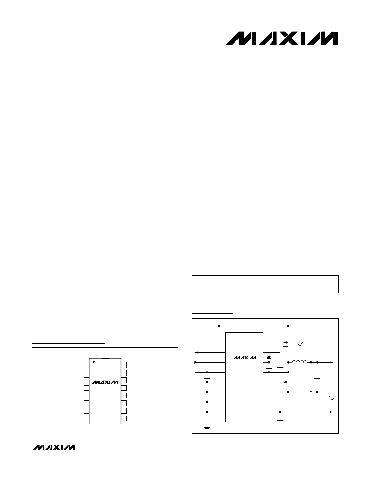
MAX1917
Tracking, Sinking and Sourcing, Synchronous Buck
Controller for DDR Memory and Termination Supplies
________________________________________________________________ Maxim Integrated Products 1
Ordering Information
MAX1917
V
IN
(2.5V TO 15V)
POK
VDDR
EN/HSD
POK
DDR
V+
REF
ILIM
FSEL
GND
DH
VL
BST
DL
LX
PGND
VTT
VTTR
V
OUT
VTTR
(4.5V TO 14V)
VL
Typical Operating Circuit
19-2335; Rev 1; 6/02
For pricing, delivery, and ordering information, please contact Maxim/Dallas Direct! at
1-888-629-4642, or visit Maxim’s website at www.maxim-ic.com.
Pin Configuration
Quick-PWM is a trademark of Maxim Integrated Products, Inc.
DDR Memory Power
Supply
Processor or DSP Core
Supply
AGTL Bus Termination
Supply
Notebook Computers
Desktop Computers
Storage
Networking Systems
PART TEMP RANGE PIN-PACKAGE
MAX1917EEE -40°C to +85°C 16 QSOP
TOP VIEW
1
EN/HSD LX
2
DDR
POK
3
4
VTT
ILIM
5
6
FSEL
7
REF
GND
8
16
15
DH
14
BST
MAX1917EEE
QSOP
13
PGND
12
DL
VL
11
10
V+
9
VTTR
Page 2
MAX1917
Tracking, Sinking and Sourcing, Synchronous Buck
Controller for DDR Memory and Termination Supplies
2 _______________________________________________________________________________________
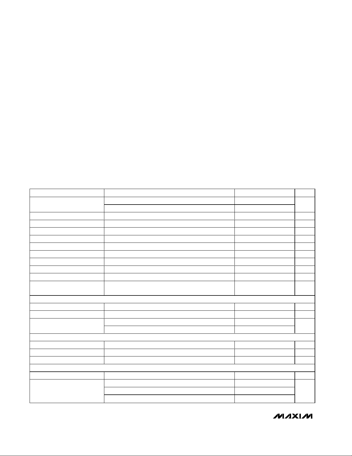
ABSOLUTE MAXIMUM RATINGS
ELECTRICAL CHARACTERISTICS
(V+ = 12V, V
EN/HSD
= V
DDR
= 2.5V, CVL= 4.7µF, C
VTTR
= 1µF, C
REF
= 0.22µF, V
FSEL
= 0, ILIM = VL, PGND = LX = POK = GND,
BST = VL. Specifications are for T
A
= 0°C to +85°C. Typical values are at TA= +25°C, unless otherwise specified.)
Stresses beyond those listed under “Absolute Maximum Ratings” may cause permanent damage to the device. These are stress ratings only, and functional
operation of the device at these or any other conditions beyond those indicated in the operational sections of the specifications is not implied. Exposure to
absolute maximum rating conditions for extended periods may affect device reliability.
V+ to GND ..............................................................-0.3V to +15V
EN/HSD to GND .....................................................-0.3V to +16V
VL to GND ................................................................-0.3V to +6V
PGND to GND .......................................................-0.3V to +0.3V
VTT, DDR, POK to GND ...........................................-0.3V to +6V
REF, VTTR, DL, ILIM, FSEL to GND ................-0.3V to VL + 0.3V
LX to PGND ............................................................-0.3V to +30V
BST to GND ............................................................-0.3V to +36V
DH to LX ......................................................-0.3V to V
BST
+ 0.3V
LX to BST..................................................................-6V to +0.3V
REF Short Circuit to GND ...........................................Continuous
Continuous Power Dissipation (T
A
= +70°C)
16-Pin QSOP (derate up to +70°C)..............................667mW
16-Pin QSOP (derating above +70°C).....................8.3mW/°C
Operating Temperature Range
Extended .........................................................-40°C to +85°C
Junction Temperature......................................................+150°C
Storage Temperature Range .............................-65°C to +150°C
Lead Temperature (soldering 10s.) .................................+300°C
V+ Input Voltage Range
EN/HSD Input Voltage Range Enabled 1.5 15.0 V
DDR Input Voltage Range 0 3.6 V
V+ Supply Current VTT = 2.0V 0.8 1.2 mA
DDR Supply Current 115 250 µA
EN/HSD Supply Current 510µA
VL Supply Current VL = V+ = 5.5V, VTT = 2.0V 0.8 1.2 mA
V+ Shutdown Supply Current EN/HSD = 0V 3 5 µA
DDR Shutdown Supply Current EN/HSD = 0V 1 µA
VL Shutdown Supply Current VL = V+ = 5.5V 3 5 µA
VL Undervoltage Lockout
Threshold
VTT
VTT Input Bias Current V
VTT Feedback Voltage Range 0 1.8 V
VTT Feedback Voltage
Accuracy
REFERENCE
Reference Output Voltage V+ = VL = 4.5V to 5.5V, I
Reference Load Regulation V+ = VL = 5V, I
Reference UVLO V+ = VL = 5V 1.5 1.6 1.7 V
VTTR
VTTR Output Voltage Range 0 1.8 V
VTTR Output Accuracy
PARAMETER CONDITIONS MIN TYP MAX UNITS
VL = V+ 4.5 5.5
Rising edge, hysteresis = 40mV 4.05 4.25 4.40 V
VTT
Overload range, V
Overload range, V
I
VTTR
I
VTTR
I
VTTR
= 2.5V -0.1 0 µA
= 1.8V 49.5 50 50.5
DDR
= 3.6V 49.5 50 50.5
DDR
REF
= 0 to 50µA 10 mV
REF
= -5mA to +5mA 49.5 50 50.5
= -25mA to +25mA, V
= -25mA to +25mA, V
= 0 1.98 2.00 2.02 V
= 1.8V 49 50 51
DDR
= 3.6V 49.5 50 50.5
DDR
5.5 14.0
%V
%V
V
DDR
DDR
Page 3
MAX1917
Tracking, Sinking and Sourcing, Synchronous Buck
Controller for DDR Memory and Termination Supplies
_______________________________________________________________________________________ 3
ELECTRICAL CHARACTERISTICS (continued)
(V+ = 12V, V
EN/HSD
= V
DDR
= 2.5V, CVL= 4.7µF, C
VTTR
= 1µF, C
REF
= 0.22µF, V
FSEL
= 0, ILIM = VL, PGND = LX = POK = GND,
BST = VL. Specifications are for T
A
= 0°C to +85°C. Typical values are at TA= +25°C, unless otherwise specified.)
PARAMETER CONDITIONS MIN TYP MAX UNITS
Thermal Shutdown Rising temperature, typical hysteresis = 15°C +160 °C
SOFT-START
ILIM Ramp Period
OSCILLATOR
Ramps the ILIM trip threshold from 20% to 100%
in 20% increments
1.7 ms
FSEL = VL 200
Oscillator Frequency
FSEL = unconnected 300
FSEL = REF 400
FSEL = GND 550
kHz
FSEL = VL 2.18 2.5 2.83
On Time (Note 1)
FSEL not connected 1.45 1.67 1.89
FSEL = REF 1.09 1.25 1.41
FSEL = GND 0.82 0.91 1.00
µs
Minimum Off Time (Note 1) 350 400 ns
CURRENT LIMIT
Current-Limit Threshold
(Positive Direction)
Current-Limit Threshold
(Negative Direction)
ILIM Input Current 5µA
V
REGULATOR
L
Output Voltage
Line Regulation 5.5V < V+ < 14V, IVL = 10mA 0.2 %
RMS Output Current 35 mA
Bypass Capacitor ESR < 100mΩ 2.2 µF
DRIVER
DH Gate-Driver On-Resistance V
DL Gate-Driver On-Resistance
(Source)
DL Gate-Driver On-Resistance
(Sink)
Dead Time
FSEL LOGIC
Logic Input Current -3 3 µA
Logic GND Level 0.5 V
Logic REF Level FSEL = VREF 1.65 2.35 V
Logic Float Level FSEL floating 3.15 3.85 V
LX to PGND, ILIM = VL 90 100 110
LX to PGND, R
LX to PGND, R
LX to PGND, ILIM = VL, with percentage of positive
current-limit threshold
5.5V < V+ < 14V
1mA < I
BST
DL high state 1.6 3 Ω
DL low state 0.75 1.25 Ω
DL rising 32
DL falling 30
< 35mA
VL
- VLX = 5V 1.4 2.5 Ω
= 100kΩ 40 50 60
ILIM
= 400kΩ 170 200 230
ILIM
-90 -110 -130 %
4.8 5.0 5.2 V
mV
ns
Page 4
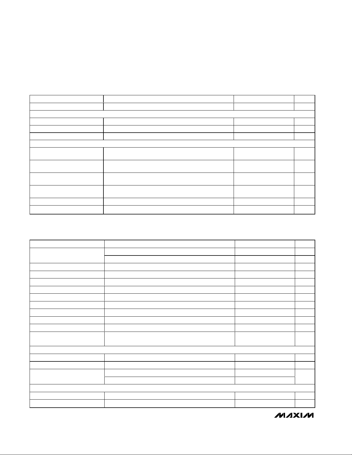
MAX1917
Tracking, Sinking and Sourcing, Synchronous Buck
Controller for DDR Memory and Termination Supplies
4 _______________________________________________________________________________________
ELECTRICAL CHARACTERISTICS (continued)
(V+ = 12V, V
EN/HSD
= V
DDR
= 2.5V, CVL= 4.7µF, C
VTTR
= 1µF, C
REF
= 0.22µF, V
FSEL
= 0, ILIM = VL, PGND = LX = POK = GND,
BST = VL. Specifications are for T
A
= 0°C to +85°C. Typical values are at TA= +25°C, unless otherwise specified.)
ELECTRICAL CHARACTERISTICS
(V+ = 12V, V
EN/HSD
= V
DDR
= 2.5V, CVL= 4.7µF, C
VTTR
= 1µF, C
REF
= 0.22µF, V
FSEL
= 0, ILIM = VL, PGND = LX = POK = GND,
BST = VL. Specifications are for T
A
= -40°C to +85°C, unless otherwise specified.) (Note 2)
Logic VL Level FSEL = VL VL - 0.4 V
EN/HSD LOGIC
EN/HSD Shutdown Current Max I
Logic High VL = V+ = 4.5V to 5.5V, 100mV hysteresis 1.45 V
Logic Low VL = V+ = 4.5V to 5.5V 0.8 V
POWER-OK OUTPUT
Upper VTT Threshold 110 112 114
Lower VTT Threshold 86 88 90
Upper VTTR Threshold 110 112 114
Lower VTTR Threshold 86 88 90
POK Output Low Level I
POK Output High Leakage V
PARAMETER CONDITIONS MIN TYP MAX UNITS
= 2mA 0.4 V
SINK
POK
for V
EN/HSD
= 5.5V 5 µA
= 0.8V 0.5 3.0 µA
EN/HSD
%V
%V
%V
%V
DDR
2
DDR
2
DDR
2
DDR
2
/
/
/
/
V+ Input Voltage Range
EN/HSD Input Voltage Range Enabled 1.5 15.0 V
DDR Input Voltage Range 0 3.6 V
V+ Supply Current VTT = 2.0V 1.2 mA
DDR Supply Current 250 µA
EN/HSD Supply Current V
VL Supply Current VL = V+ = 5.5V 1.2 mA
V+ Shutdown Supply Current EN/HSD = 0V 5 µA
DDR Shutdown Supply Current EN/HSD = 0V 1 µA
VL Shutdown Supply Current VL = V+ = 5.5V 5 µA
VL Undervoltage Lockout
Threshold
VTT
VTT Input Bias Current V
VTT Feedback Voltage Range 0 1.8 V
VTT Feedback Voltage
Accuracy
REFERENCE
Reference Output Voltage V+ = VL = 4.5V to 5.5V, I
Reference Load Regulation V+ = VL = 5V, I
PARAMETER CONDITIONS MIN TYP MAX UNITS
VL = V+ 4.5 5.5 V
EN/HSD
Rising edge, hysteresis = 40mV 4.05 4.40 V
VTT
Overload range, V
Overload range, V
= 2.5V 10 µA
= 2.5V -0.15 0 µA
= 1.8V 49.5 50.5
DDR
= 3.6V 49.5 50.5
DDR
REF
= 0 to 50µA 10 mV
REF
= 0 1.98 2.02 V
5.5 14.0 V
%V
DDR
Page 5
MAX1917
Tracking, Sinking and Sourcing, Synchronous Buck
Controller for DDR Memory and Termination Supplies
_______________________________________________________________________________________ 5
ELECTRICAL CHARACTERISTICS (continued)
(V+ = 12V, V
EN/HSD
= V
DDR
= 2.5V, CVL= 4.7µF, C
VTTR
= 1µF, C
REF
= 0.22µF, V
FSEL
= 0, ILIM = VL, PGND = LX = POK = GND,
BST = VL. Specifications are for T
A
= -40°C to +85°C, unless otherwise specified.) (Note 2)
Reference UVLO V+ = VL = 5V 1.5 1.7 V
VTTR
VTTR Output Voltage Range 0 1.8 V
OSCILLATOR
PARAMETER CONDITIONS MIN TYP MAX UNITS
On Time (Note 1)
I
VTTR
I
VTTR
I
VTTR
FSEL = VL 2.18 2.83
FSEL not connected 1.45 1.89
FSEL = REF 1.09 1.41
FSEL = GND 0.82 1.00
= -5mA to +5mA 49.5 50.5
= -25mA to +25mA, V
= -25mA to +25mA, V
DDR
DDR
= 1.8V 49 51VTTR Output Accuracy
= 3.6V 49.5 50.5
%V
DDR
µs
Minimum Off Time (Note 1) 400 ns
CURRENT LIMIT
Current-Limit Threshold
(Positive Direction)
Current-Limit Threshold
(Negative Direction)
LX to PGND, ILIM = VL 85 110
LX to PGND, R
LX to PGND, R
LX to PGND, ILIM = VL, with percentage of positive
current-limit threshold
= 100kΩ 35 60
ILIM
= 400kΩ 160 230
ILIM
-90 -130 %
mV
VL REGULATOR
Output Voltage 5.5V < V+
< 14V; 1mA < I
< 35mA 4.8 5.2 V
VL
RMS Output Current 35 mA
Bypass Capacitor ESR < 100mΩ 2.2 µF
FSEL LOGIC
Logic Input Current 3µA
Logic GND Level 0.5 V
Logic REF Level FSEL = VREF 1.65 2.35 V
Logic Float Level FSEL floating 3.15 3.85 V
Logic VL Level FSEL = VL VL - 0.4 V
EN/HSD LOGIC
EN/HSD Shutdown Current I
Logic High VL = V+ = 4.5V to 5.5V, 100mV hysteresis 1.45 V
Logic Low VL = V+ = 4.5V to 5.5V 0.8 V
POWER-OK OUTPUT
Upper VTT Threshold 110 114
Lower VTT Threshold 86 90
EN/HSD
for V
= 0.8V 0.5 3.0 µA
EN/HSD
%V
%V
DDR
/2
DDR
/2
Page 6
Note 1: On Time and Off Time specifications are measured from 50% point to 50% point at the DH pin with LX forced to 0V, BST
forced to 5V, and a 250pF capacitor connected from DH to LX. Actual in-circuit times may differ due to MOSFET switching
speeds.
Note 2: Specifications to -40°C are guaranteed by design and are not production tested.
MAX1917
Tracking, Sinking and Sourcing, Synchronous Buck
Controller for DDR Memory and Termination Supplies
6 _______________________________________________________________________________________
ELECTRICAL CHARACTERISTICS (continued)
(V+ = 12V, V
EN/HSD
= V
DDR
= 2.5V, CVL= 4.7µF, C
VTTR
= 1µF, C
REF
= 0.22µF, V
FSEL
= 0, ILIM = VL, PGND = LX = POK = GND,
BST = VL. Specifications are for T
A
= -40°C to +85°C, unless otherwise specified.) (Note 2)
Typical Operating Characteristics
(V+ = 12V, V
OUT
= 1.25V, TA= +25°C, unless otherwise noted.)
PARAMETER CONDITIONS MIN TYP MAX UNITS
Upper VTTR Threshold 110 114
Lower VTTR Threshold 86 90
POK Output Low Level I
POK Output High Leakage V
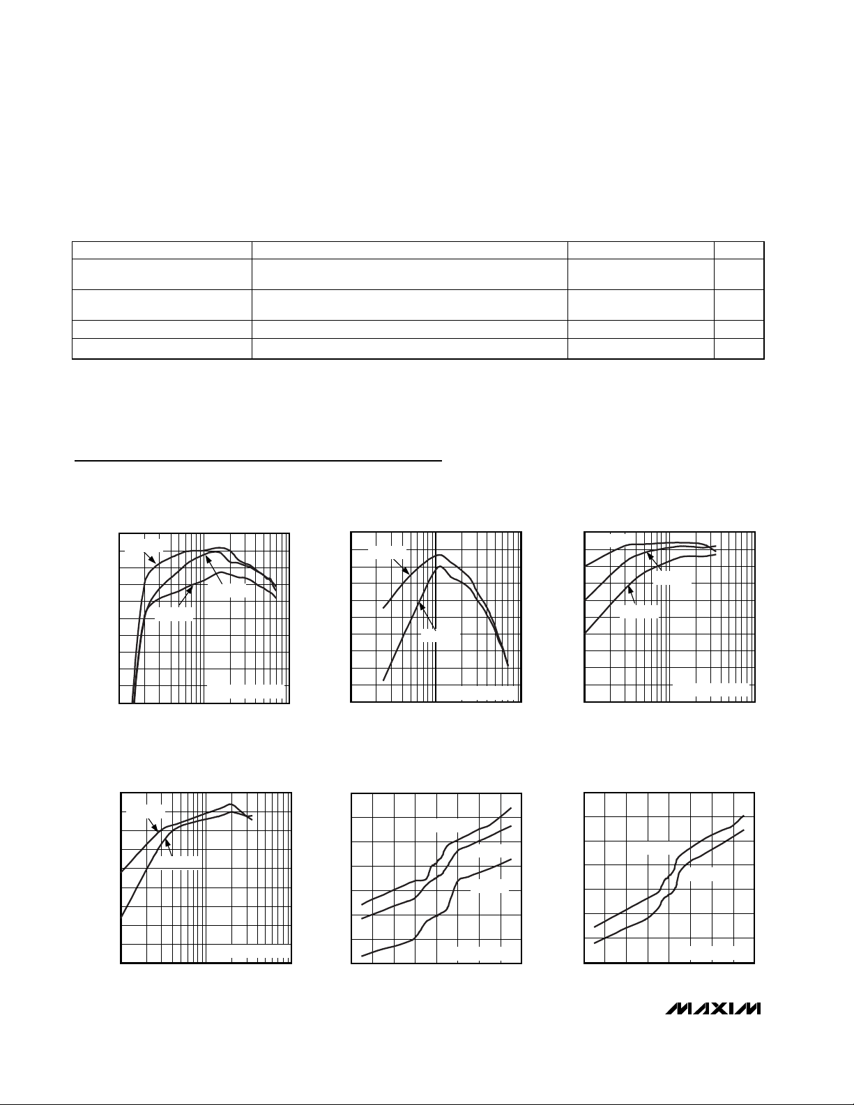
EFFICIENCY vs. LOAD CURRENT
100
VIN = 2.5V
95
90
85
80
75
70
EFFICIENCY (%)
65
60
55
50
0.1 1.0 10.0
= 2mA 0.4 V
SINK
POK
= 5.5V 5 µA
AT 1.25V OUTPUT
96
94
MAX1917 toc01
92
VIN = 5V
VIN = 2V
CIRCUIT OF FIGURE 3
LOAD CURRENT (A)
90
88
86
84
EFFICIENCY (%)
82
80
78
76
0.1 1.0 10.0
EFFICIENCY vs. LOAD CURRENT
AT 0.9V OUTPUT
VIN = 2.5V
VIN = 5V
CIRCUIT OF FIGURE 3
LOAD CURRENT (A)
EFFICIENCY vs. LOAD CURRENT
AT 1.25V OUTPUT
100
VIN = 2.5V
90
MAX1917 toc02
80
70
60
50
40
EFFICIENCY (%)
30
20
10
0
0.1 1.0 10.0
VIN = 5V
VIN = 12V
CIRCUIT OF FIGURE 4
LOAD CURRENT (A)
%V
%V
DDR
/2
DDR
/2
MAX1917 toc03
EFFICIENCY vs. LOAD CURRENT
AT 0.9V OUTPUT
95
90
VIN = 2.5V
85
80
75
70
EFFICIENCY (%)
65
60
55
50
0.1 1.0 10.0
VIN = 5V
CIRCUIT OF FIGURE 4
LOAD CURRENT (A)
MAX1917 toc04
FREQUENCY vs. LOAD CURRENT
AT 1.25V OUTPUT
650
600
550
500
450
FREQUENCY (kHz)
400
350
300
-8 -4 -2-6 02468
VIN = 2.5V
VIN = 5V
VIN = 12V
CIRCUIT OF FIGURE 3
LOAD CURRENT (A)
MAX1917 toc05
FREQUENCY (kHz)
FREQUENCY vs. LOAD CURRENT
AT 0.9V OUTPUT
650
600
550
500
450
400
350
300
-8 -2 0-6-4 2468
VIN = 2.5V
LOAD CURRENT (A)
MAX1917 toc06
VIN = 5V
CIRCUIT OF FIGURE 3
Page 7

MAX1917
Tracking, Sinking and Sourcing, Synchronous Buck
Controller for DDR Memory and Termination Supplies
_______________________________________________________________________________________ 7
Typical Operating Characteristics (continued)
(V+ = 12V, V
OUT
= 1.25V, TA= +25°C, unless otherwise noted.)
FREQUENCY vs. INPUT VOLTAGE
650
600
550
500
450
FREQUENCY (kHz)
400
350
CIRCUIT OF FIGURE 3
300
157391311 15
I
= 7A
OUT
I
= 0.1A
OUT
INPUT VOLTAGE (V)
SHUTDOWN CURRENT
vs. INPUT VOLTAGE
2.5
2.3
2.1
1.9
1.7
1.5
1.3
1.1
SHUTDOWN CURRENT (mA)
0.9
0.7
0.5
13579111315
CIRCUIT OF FIGURE 3
INPUT VOLTAGE (V)
SHUTDOWN CURRENT
vs. INPUT VOLTAGE
CIRCUIT OF FIGURE 6
INPUT VOLTAGE (V)
LOAD REGULATION WITH
DROOP RESISTOR
V
= 2.5V
DDR
VIN = 12V
VIN = 2.5V
LOAD CURRENT (A)
VIN = 5V
540
538
MAX1917 toc07
536
534
532
530
528
FREQUENCY (kHz)
526
524
522
520
1.32
1.31
MAX1917 toc10
1.30
1.29
1.28
1.27
1.26
OUTPUT VOLTAGE (V)
1.25
1.24
1.23
1.22
FREQUENCY vs. TEMPERATURE
I
= 3.5A
LOAD
CIRCUIT OF FIGURE 3
-40 -20 0 20 40 60 80 100
TEMPERATURE (°C)
LOAD REGULATION WITHOUT
DROOP RESISTOR
V
= 2.5V
DDR
VIN = 5V
VIN = 2.5V
-7 -3 -1-5 1357
LOAD CURRENT (A)
VIN = 12V
4.0
3.5
MAX1917 toc08
3.0
2.5
2.0
SHUTDOWN CURRENT (µA)
1.5
1.0
1.35
1.33
MAX1917 toc11
1.31
1.29
1.27
1.25
1.23
OUTPUT VOLTAGE (V)
1.21
1.19
1.17
1.15
1793 5 11 13 15
-8 -4 -2-6 02468
MAX1917 toc09
MAX1917 toc12
TRANSIENT LOAD RESPONSE
WITHOUT DROOP RESISTOR
OA
CIRCUIT OF FIGURE 3
TRANSIENT LOAD RESPONSE
20µs/div
MAX1917 toc13
V
VTT
50mV/div
I
OUT
5A/div
WITH DROOP RESISTOR
0A
CIRCUIT OF FIGURE 3
20µs/div
MAX1917 toc14
V
VTT
50mV/div
I
OUT
5A/div
POWER-UP WITH V
400µs/div
TRACKING
DDR
MAX1917 toc15
V
OUT
1V/div
V
POK
5V/div
V
DDR
2.5V
V
EN/HSD
10V/div
Page 8

Pin Description
MAX1917
Tracking, Sinking and Sourcing, Synchronous Buck
Controller for DDR Memory and Termination Supplies
8 _______________________________________________________________________________________
Typical Operating Characteristics (continued)
(V+ = 12V, V
OUT
= 1.25V, TA= +25°C, unless otherwise noted.)
CURRENT LIMIT vs. TEMPERATURE
18
16
14
12
10
CURRENT LIMIT (A)
R
= 402kΩ
ILIM
8
6
R
= 200kΩ
ILIM
4
2
0
-40 100
TEMPERATURE (°C)
INDUCTOR PEAK AND VALLEY CURRENT
vs. INPUT VOLTAGE AT CURRENT LIMIT
18
R
= 400kΩ
ILIM
MAX1917 toc16
806020 400-20
16
14
12
INDUCTOR CURRENT (A)
10
CIRCUIT OF FIGURE 3
8
115
I
VALLEY
I
PEAK
VIN (V)
MAX1917 toc17
13119753
PIN NAME FUNCTION
1 EN/HSD
2 DDR
3 POK
4 VTT VTT Feedback Input. Connect to VTT output.
5 ILIM
6 FSEL Frequency Select. Selects the switching frequency of the MAX1917. See Table 1 for configuration of FSEL.
7 REF Reference Bypass. Connect a 0.22µF or larger capacitor from REF to GND.
8 GND Ground
9 VTTR
10 V+
11 VL
12 DL Low-Side MOSFET Gate Drive. Connect to the gate of the low-side N-channel MOSFET.
13 PGND Power Ground
14 BST
15 DH High-Side MOSFET Gate Drive. Connect to the high-side N-channel MOSFET gate.
16 LX Inductor Switching Node
Enable/High-Side Drain. Connect to the high-side N-FET drain for normal operation. Leave unconnected or
connect to GND for low-power shutdown.
DDR Reference Input. An applied voltage at DDR sets V
VTT
and V
VTTR
to 1/2V
. DDR voltage range is
DDR
from 0 to 3.6V.
Power-OK Output. POK is an open-drain output and is logic high when both VTT and VTTR are within 12%
of regulation. POK is pulled low in shutdown.
Current-Limit Threshold Adjustment. Connect a resistor from ILIM to GND to set the current-limit threshold,
or connect ILIM to VL for default setting. See the Setting the Current Limit section.
VTTR Reference Output. Connect a 1µF or larger capacitor from VTTR to GND. VTTR is capable of
sourcing and sinking up to 25mA.
Input Supply Voltage. Supply input for the VL regulator and the VTTR regulator. Bypass with a 0.22µF or
larger capacitor.
Internal Regulator Output. Connect a 2.2µF or larger capacitor from VL to GND. VL can be connected to
V+ if the operating range is 4.5V to 5.5V.
Bootstrapped Supply to Drive High-Side N-Channel MOSFET. Connect a 0.47µF or larger capacitor from
BST to LX.
Page 9

MAX1917
Tracking, Sinking and Sourcing, Synchronous Buck
Controller for DDR Memory and Termination Supplies
_______________________________________________________________________________________ 9
Functional Diagram
DDR
EN/HSD
POK
ON TIME
COMPUTE
TON
TRIG Q
1-SHOT
ILIM
1-SHOT
VTTFSEL
TRIGQ
5µA
S
Q
R
Σ
BST
DH
LX
VL
DL
PGND
5V
REF
2V
REF
MAX1917
VTTR
VTT
V+
VL
REF
GND
Page 10

MAX1917
Tracking, Sinking and Sourcing, Synchronous Buck
Controller for DDR Memory and Termination Supplies
10 ______________________________________________________________________________________
Detailed Description
Internal Linear Regulator (VL)
An internal regulator produces the 5V supply (VL) that
powers the PWM controller, MOSFET driver, logic, reference, and other blocks within the IC. This 5V lowdropout (LDO) linear regulator supplies up to 35mA for
MOSFET gate-drive and external loads. For supply voltages between 4.5V and 5.5V, connect VL to V+. This
bypasses the VL regulator, which improves efficiency,
and allows the IC to function at lower input voltages.
On-Time One-Shot and
Switching Frequency
The heart of the PWM is the one-shot that sets the highside switch on time. This fast, low-jitter, adjustable oneshot includes circuitry that varies the on time in response
to both input and output voltages. The high-side switch
on time is inversely proportional to the input voltage as
measured by the EN/HSD input, and is directly proportional to the VTT output voltage. This algorithm results in
a nearly constant switching frequency despite the lack
of a fixed-frequency clock generator. The switching frequency can be selected to avoid noise-sensitive regions
such as the 455kHz IF band. Also, with a constant
switching frequency, the inductor ripple-current operating point remains relatively constant, resulting in easy
design methodology and predictable output voltage ripple. The general formula for on time (tON) is:
where V
HSD
and V
DDR
are the voltages measured at
EN/HSD and DDR, respectively, and K = 1.7µs. The
value of N depends on the configuration of FSEL and is
listed in Table 1.
The actual switching frequency, which is given by the
following equation, varies slightly due to voltage drop
across the on-resistance of the MOSFETs and the DC
resistance of the output inductor:
where I
O
is the output current, R
DSONH
is the on-resis-
tance of the high-side MOSFET, R
DSONL
is the onresistance of the low-side MOSFET, and RDCis the DC
resistance of the output inductor. The above equation is
valid only when FSEL is connected to ground. The ideal
switching frequency for V
DDR
= 2.5V is about 550kHz.
The switching frequency, which is almost constant,
results in relatively constant inductor ripple current
regardless of input voltage and predictable output voltage ripple. This feature eases design methodology.
Switching frequency increases for positive (sourcing)
load current and decreases for negative (sinking) load
current, due to the changing voltage drop across the
low-side MOSFET, which changes the inductor-current
discharge ramp rate. The on times guaranteed in the
Electrical Characteristics tables are also influenced by
switching delays caused by the loading effect of the
external power MOSFETs.
VTTR Reference
The MAX1917 VTTR output is capable of sourcing or
sinking up to 25mA of current. The V
TTR
output voltage
is one half of the voltage applied to the DDR input.
Bypass VTTR with at least a 1.0µF capacitor.
EN/HSD Function
In order to reduce pin count and package size, the
MAX1917 features a dual-function input pin, EN/HSD.
When EN/HSD is connected to ground, the internal circuitry powers off, reducing current consumption to less
than 5µA typical (circuit of Figure 6). To enable normal
operation, connect EN/HSD to the drain of the high-side
MOSFET. If EN/HSD is not grounded, it becomes an
input that monitors the high-side MOSFET drain voltage
(converter input voltage) and uses that measurement to
calculate the appropriate on time for the converter.
Therefore, EN/HSD must be connected to this node in
order for the controller to operate properly.
Table 1. Configuration of FSEL
.
VIR R
tKN
=×× ×
ON
V
1
HSD
V
DDR
2
s
µ
×+ +
f
=
S
tVIR R
ON IN O DSONL DSONH
DDR O DSONL DC
×+ −
()
()
×0510
()
3
kHz
FSEL CONNECTED
TO
N t
(µs) FREQUENCY (kHz) CONDITION
ON
Ground 1.00 0.91 550 0.5V
REF 1.33 1.25 400 0.5V
Floating 2.00 1.66 300 0.5V
VL 3.00 2.50 200 0.5V
DDR
DDR
DDR
DDR
/ V
/ V
/ V
/ V
HSD
HSD
HSD
HSD
= 0.5
= 0.5
= 0.5
= 0.5
Page 11

MAX1917
Tracking, Sinking and Sourcing, Synchronous Buck
Controller for DDR Memory and Termination Supplies
______________________________________________________________________________________ 11
Voltage Reference
The voltage at REF is nominally 2.00V. Connect a 0.22µF
ceramic bypass capacitor between REF and GND.
Overcurrent Protection
The current-limit circuit employs a unique “valley” current-sensing algorithm that uses the on-state resistance
of the low-side MOSFET as a current-sensing element.
If the current-sense signal is greater than the currentlimit threshold, the PWM is not allowed to initiate a new
cycle. The actual peak current is greater than the current-limit threshold by an amount equal to the inductor
ripple current. Therefore, the exact current-limit characteristic and maximum load capability are a function of
the MOSFET on-resistance, inductor value, and input
voltage. The reward for this uncertainty is robust, lossless overcurrent sensing. There is also a negative current limit that prevents excessive reverse inductor
currents when V
OUT
is sinking current. The negative
current-limit threshold is set to approximately 110% of
the positive current limit, and tracks the positive current
limit when ILIM is adjusted. The current-limit threshold
can be adjusted with an external resistor (R
ILIM
) at ILIM.
A precision 5µA pullup current source at ILIM sets a
voltage drop on this resistor, adjusting the current-limit
threshold from <50mV to >200mV. In the adjustable
mode, the current-limit threshold voltage is precisely
1/10th the voltage seen at ILIM.
Therefore, choose R
ILIM
equal to 2kΩ/mV of the cur-
rent-limit threshold. The threshold defaults to 100mV
when ILIM is connected to VL. The logic threshold for
switchover to the 100mV default value is approximately
V
L
- 1V. The adjustable current limit can accommodate
various MOSFETs. A capacitor in parallel with R
ILIM
can
provide a variable soft-start function.
Carefully observe the PC board layout guidelines to
ensure that noise and DC errors do not corrupt the current-sense signals seen by LX and PGND. The IC must
be mounted close to the low-side MOSFET with short,
direct traces making a Kelvin-sense connection to the
source and drain terminals. See the PC Board Layout
section.
Voltage Positioning
The quick-PWM control architecture responds virtually
instantaneously to transient load changes and eliminates the control loop delay of conventional PWM controllers. As a result, a large portion of the voltage
deviation during a step load change is from the equivalent series resistance (ESR) of the output capacitors.
For DDR termination applications, the maximum
allowed voltage deviation is ±40mV for any output load
transition from sourcing current to sinking current.
Passive voltage positioning adjusts the converter’s output voltage based on its load current to optimize transient response and minimize the required output
capacitance. Voltage positioning is implemented by
connecting a 2mΩ resistor as shown in Figure 1.
MOSFET Drivers
The DH and DL drivers are optimized for driving moderate-size, high-side and larger, low-side power
MOSFETs and are optimized for 2.5V and 5V input voltages. The drivers are sized to drive MOSFETs that can
deliver up to 25A output current. An adaptive deadtime circuit monitors the DL output and prevents the
Figure 2. Increasing the On Time of the High-Side MOSFET
Figure 1. Using a Resistor for Voltage Positioning
V
POK
V+
MAX1917
DDR
EN/HSD
REF
ILIM
FSEL
GND
VL
BST
DH
LX
DL
PGND
VTT
VTTR
4 x 270µF
IN
R
2mΩ
BST
PGND
VTT
VTTR
VL
R
BST
DH
LX
DL
POK
V+
MAX1917
DDR
DRP
V
OUT
2V
VTTR
EN/HSD
REF
ILIM
FSEL
GND
Page 12

MAX1917
Tracking, Sinking and Sourcing, Synchronous Buck
Controller for DDR Memory and Termination Supplies
12 ______________________________________________________________________________________
high-side FET from turning on until DL is fully off. There
must be a low-resistance, low-inductance path from the
DL driver to the MOSFET gate in order for the adaptive
dead-time circuit to work properly. Otherwise, the
sense circuitry in the MAX1917 interprets the MOSFET
gate as off while there is actually still charge left on the
gate. Use very short, wide traces measuring 10
squares to 20 squares (50mils to 100mils wide if the
MOSFET is 1in from the MAX1917). The dead time at
the other edge (DH turning off) is determined by a fixed
35ns (typ) internal delay. The internal pulldown transistor that drives DL low is robust, with a 0.5Ω (typ) on-
resistance. This helps prevent DL from being pulled up
during the fast rise time of the inductor node, due to
capacitive coupling from the drain to the gate of the
massive low-side synchronous-rectifier MOSFET. Some
combinations of high- and low-side FETs may be
encountered that cause excessive gate-drain coupling,
which can lead to efficiency-killing, EMI-producing
shoot-through currents. This can often be remedied by
adding a resistor (R
BST
) in series with BST, which
increases the turn-on time of the high-side FET without
degrading the turn-off time (Figure 2).
Figure 3. Typical Application Circuit for 1.25V at 7A Output
Typical Application Circuits
R2
5.1kΩ
MAX1917
V+
V
DDR
SHDN
POK
2N7002K
VL
R3
20kΩ
5.5V TO 14V
C9
0.47µF/25V
0.47µF/10V
Q3
3
POK
10
V+
2
DDR
1
EN/HSD
C8
7
REF
5
VL
ILIM
6
FSEL
8
GND
BST
PGND
VTT
VTTR
VL
2.5V
V
V
OUT
PGND
VTTR
IN
11
VL
DH
LX
DL
D1
CMPSH-3
14
C4
0.47µF
15
10V
16
12
13
4
9
C7
1µF/6.3V
C3
4.7µF
10V
2.5V
Q1
IRF7463
0.68µH/9A
Q2
IRF7463
C2
2 x 330µF
6V
L1
6 x 270µF
C1
1µF
6.3V
1.25V AT 7A
C6
2V
C5
2 x 10µF
6.3V
OUTPUT CAPACITORS ARE SELECTED TO COMPLY WITH JEDEC SPECIFICATIONS.
Page 13

MAX1917
Tracking, Sinking and Sourcing, Synchronous Buck
Controller for DDR Memory and Termination Supplies
______________________________________________________________________________________ 13
Typical Application Circuits (continued)
Figure 5. Typical Application Circuit for 1.25V at 3.5A Output
Figure 4. Typical Application Circuit for 1.25V at 7A Output Using Voltage Positioning
R2
5.1kΩ
MAX1917
VL
BST
DH
LX
DL
PGND
VTT
VTTR
V+
V
DDR
SHDN
POK
2N7002K
Q3
VL
R3
20kΩ
5.5V TO 14V
C9
0.47µF/25V
0.47µF/10V
VL
3
POK
10
V+
2
DDR
1
EN/HSD
C8
7
REF
5
ILIM
6
FSEL
8
GND
R2
5.1kΩ
MAX1917
VL
BST
DH
LX
DL
PGND
VTT
VTTR
V+
V
DDR
SHDN
POK
Q3
2N7002K
VL
R3
20kΩ
5.5V TO 14V
C9
0.47µF/25V
0.47µF/10V
VL
3
POK
10
V+
2
DDR
1
EN/HSD
C8
7
REF
5
ILIM
6
FSEL
8
GND
VL
11
D1
CMPSH-3
14
C4
0.47µF
15
10V
16
12
13
4
9
C7
1µF/6.3V
OUTPUT CAPACITORS ARE SELECTED TO COMPLY WITH JEDEC SPECIFICATIONS
VL
11
D1
CMPSH-3
14
C4
0.22µF
15
10V
16
12
13
4
9
C7
1µF/6.3V
C3
4.7µF
10V
2.5V
C3
2.2µF
10V
2.5V
Q1
IRF7463
0.68µH/9A
Q2
IRF7463
Q1
IRF7811W
Q2
IRF7811W
C2
2 x 330µF
6V
L1
C2
330µF
6V
L1
1.0µH/5A
3 x 270µF
C6
2V
C1
1µF
6.3V
1.25V AT 7A
2mΩ
C1
1µF
6.3V
1.25V AT 3.5A
C5
10µF
6.3V
2.5V
C6
4 x 270µF
2V
2.5V
V
V
OUT
PGND
VTTR
V
PGND
VTTR
V
OUT
IN
IN
OUTPUT CAPACITORS ARE SELECTED TO COMPLY WITH JEDEC SPECIFICATIONS.
Page 14

MAX1917
Tracking, Sinking and Sourcing, Synchronous Buck
Controller for DDR Memory and Termination Supplies
14 ______________________________________________________________________________________
Figure 7. Circuit to Generate a Fixed 2.5V at 12A Output with a Wide Input Voltage Range
Figure 6. Typical Application Circuit Using P/N-Channel MOSFETs for EN to Minimize the Supply Current from VINin Shutdown Mode
Typical Application Circuits (continued)
R2
10kΩ
VL
SHDN
V
20kΩ`
POK
V+
DDR
R3
Q3
Si1029X
5.5V TO 14V
C9
0.47µF/25V
VL
C8
0.47µF/10V
VL
3
POK
10
V+
2
MAX1917
DDR
1
EN/HSD
7
REF
5
ILIM
6
FSEL
8
GND
11
VL
BST
DH
LX
PGND
VTT
VTTR
D1
CMPSH-3
14
C4
0.22µF
10V
15
16
12
DL
13
4
9
C7
1µF/10V
OUTPUT CAPACITORS ARE SELECTED TO COMPLY WITH JEDEC SPECIFICATIONS.
C3
2.2µF
10V
2.5V
Q1
IRF7811W
1.0µH/5A
Q2
IRF7811W
C2
330µF
6V
L1
3 x 270µF
C6
2V
C1
1µF
6.3V
1.25V AT 3.5A
C5
10µF
6.3V
2.5V
V
V
OUT
PGND
VTTR
IN
SHDN
2N7002K
5V
R3
20kΩ
POK
C9
0.22µF
25V
C8
R6
0.47µF/10V
Q3
3
POK
10
V+
2
DDR
1
EN/HSD
7
REF
5
VL
ILIM
6
FSEL
8
GND
R2
5.1kΩ
MAX1917
BST
PGND
VTT
VTTR
4.5V TO 15V
11
VL
DH
LX
D1
CMPSH-3
14
C4
0.47µF
15
10V
16
C3
4.7µF
10V
2.5V
12
DL
Q1
IRF7822
0.75µH/24A
Q2
IRF7822
C2
4 x 330µF
6V
L1
13
4
C1
1µF
25V
R4
15kΩ
0.1%
R5
10kΩ
0.1%
C6
3 x 560µF
4V
2.5V AT 12A
C5
1µF
6.3V
9
V
OUT
PGND
V
IN
OUTPUT CAPACITORS ARE SELECTED TO COMPLY WITH JEDEC SPECIFICATIONS
Page 15

MAX1917
Tracking, Sinking and Sourcing, Synchronous Buck
Controller for DDR Memory and Termination Supplies
______________________________________________________________________________________ 15
Design Procedure
Firmly establish the input voltage range and maximum
load current before choosing a switching frequency
and inductor operating point (ripple current ratio). The
primary design trade-off is in choosing a good switching frequency and inductor operating point, and the following four factors dictate the rest of the design:
1) Input Voltage Range. The maximum value
(V
IN(MAX)
) must accommodate the worst-case high
input voltage. The minimum value (V
IN(MIN)
) must
account for the lowest input voltage after drops due
to connectors, fuses, and battery selector switches.
If there is a choice at all, lower input voltages result
in better efficiency.
2) Maximum Load Current. There are two values to
consider. The peak load current (I
LOAD(MAX)
)
determines the instantaneous component stresses
and filtering requirements, and thus drives output
capacitor selection, inductor saturation rating, and
the design of the current-limit circuit. The continuous load current (I
LOAD
) determines the thermal
stresses and thus drives the selection of input
capacitors, MOSFETs, and other critical heat-contributing components.
3) Switching Frequency. This determines the basic
trade-off between size and efficiency. The optimal
frequency is largely a function of maximum input
voltage, due to MOSFET switching losses that are
proportional to frequency and V
IN
2
. The optimum
frequency is also a moving target, due to rapid
improvements in MOSFET technology that are making higher frequencies more practical.
4) Inductor Operating Point. This provides trade-offs
between size and efficiency. Low inductor values
cause large ripple currents, resulting in the smallest
size but poor efficiency and high output noise. The
minimum practical inductor value is one that causes
the circuit to operate at the edge of critical conduction (where the inductor current just touches zero
with every cycle at maximum load). Inductor values
lower than this grant no further size-reduction benefit.
The inductor ripple current also impacts transientresponse performance, especially at low V
IN
- V
OUT
differentials. Low inductor values allow the inductor
current to slew faster, replenishing charge removed
from the output filter capacitors by a sudden load step.
The amount of output sag is also a function of the maximum duty factor, which can be calculated from the on
time and minimum off time:
Output Inductor Selection
The switching frequency (on time) and operating point
(% ripple or LIR) determine the inductor value as follows:
Example: I
LOAD(MAX)
= 7A, V
OUT
= 1.25V, f = 550kHz,
50% ripple current or LIR = 0.5:
Find a low-loss inductor having the lowest possible DC
resistance that fits in the allotted dimensions. Ferrite
cores are often the best choice, although powdered
iron is inexpensive and can work well at 200kHz. The
core must be large enough not to saturate at the peak
inductor current:
(I
PEAK
): I
PEAK
= I
LOAD(MAX)
+ (LIR / 2) (I
LOAD(MAX)
)
Output Capacitor Selection
The output filter capacitor must have low enough ESR
to meet output ripple and load-transient requirements,
yet have high enough ESR to satisfy stability requirements. Also, the capacitance value must be high
enough to absorb the inductor energy going from a
positive full-load to negative full-load condition or vice
versa without incurring significant over/undershoot. In
DDR termination applications where the output is subject to violent load transients, the output capacitor’s
size depends on how much ESR is needed to prevent
the output from dipping too low under a load transient.
Ignoring the sag due to finite capacitance:
In DDR applications, V
DIP
= 40mV, the output capacitor’s size depends on how much ESR is needed to
maintain an acceptable level of output voltage ripple:
2
IL
∆
()
LOAD MAX
V
SAG
=
×× × −
C DUTY V V
2
f IN MIN OUT
()
L
=
L
550 0 5 7
kHz A
f LIR I
125
V
OUT
××
V
.
××
.
R
ESR
R
≤
ESR
V
DIP
≤==Ω
I
LOAD MAX
()
V
PP
−
×
LIR I
LOAD MAX
()
×
()
()
LOAD MAX
()
065 068
=µ µ
..
mV
40
A
14
mV
9
=
×
.
05 7
kHz
HH=
()
.
m
285
=Ω
.
m
257
A
Page 16

MAX1917
Tracking, Sinking and Sourcing, Synchronous Buck
Controller for DDR Memory and Termination Supplies
16 ______________________________________________________________________________________
The actual microfarad capacitance value required
relates to the physical size needed to achieve low ESR,
as well as to the chemistry of the capacitor technology.
As a result, the capacitor is usually selected by ESR
and voltage rating rather than by capacitance value
(this is true of tantalums, OS-CONs, POSCAPs, and
other electrolytics).
Input Capacitor Selection
The input capacitor must meet the ripple current
requirement (I
RMS
) imposed by the switching currents.
Nontantalum chemistries (ceramic, aluminum, or OSCON) are preferred due to their superior surge current
capacity:
Setting the Current Limit
The minimum current-limit threshold must be great
enough to support the maximum load current when the
current limit is at the minimum tolerance value. The valley of the inductor current occurs at I
LOAD(MAX)
minus
half of the ripple current. For example:
I
LIMIT(LOW)
> I
LOAD(MAX)
- (LIR / 2) ✕ I
LOAD(MAX)
where I
LIMIT(LOW)
= minimum current-limit threshold
voltage divided by the R
DS(ON)
of Q2. For the
MAX1917, the minimum current-limit threshold (100mV
default setting) is 50mV. Use the worst-case maximum
value for R
DS(ON)
from the MOSFET Q2 data sheet, and
add some margin for the rise in R
DS(ON)
with temperature. A good general rule is to allow 0.5% additional
resistance for each °C of temperature rise.
When adjusting the current limit, use a 1% tolerance
R
ILIM
resistor to prevent a significant increase of errors
in the current-limit tolerance.
Setting the Voltage Positioning
The droop resistor, R
DRP
, in series with the output
inductor before the output capacitor, sets the droop
voltage, V
DRP
. Choose R
DRP
such that the output voltage at the maximum load current, including ripple, is
just above the lower limit of the output tolerance:
R
DRP
introduces some power dissipation, which is
given by:
PD(DRP) = R
DRP
✕ I
OUT(MAX)
2
R
DRP
should be chosen to handle this power dissipation.
MOSFET Power Dissipation
Worst-case conduction losses occur at the duty-factor
extremes. For the high-side MOSFET, the worst-case
power dissipation due to resistance occurs at minimum
input voltage:
PD(Q1) = (V
OUT
/ V
IN(MIN)
) ✕ (I
LOAD
2
) ✕ (R
DS(ON)
)
Generally, a small high-side MOSFET is desired in order
to reduce switching losses at high input voltages.
However, the R
DS(ON)
required to stay within package
power-dissipation limits often limits how small the
MOSFET can be. Again, the optimum occurs when the
switching (AC) losses equal the conduction (R
DS(ON)
)
losses. Calculating the power dissipation in Q1 due to
switching losses is challenging because it must allow for
difficult-to-quantify factors that influence the turn-on and
turn-off times. These factors include the internal gate
resistance, gate charge, threshold voltage, source
inductance, and PC board layout characteristics. The following switching loss calculation provides only a very
rough estimate and is no substitute for breadboard evaluation, preferably including a check using a thermocouple mounted on Q1:
where C
RSS
is the reverse transfer capacitance of Q1
and I
GATE
is the peak gate-drive source/sink current.
For the low-side MOSFET, Q2, the worst-case power
dissipation always occurs at maximum input voltage:
PD(Q2) = (1 - V
OUT
/ V
IN(MAX)
) ✕ I
LOAD
2
✕ R
DS(ON)
II
RMS LOAD
VVV
OUT IN OUT
=×
×−
()
V
IN
R
VVV
OUT TYP OUT MIN RIPPLE
<
DRP
−−
() ()
I
()
OUT MAX
/2
PD SWITCHING
()
CV fI
×××
RSS IN MAX LOAD
=
2
()
I
GATE
Page 17

MAX1917
Tracking, Sinking and Sourcing, Synchronous Buck
Controller for DDR Memory and Termination Supplies
______________________________________________________________________________________ 17
The absolute worst case for MOSFET power dissipation
occurs under heavy overloads that are greater than or
equal to I
LOAD(MAX)
. To protect against this condition,
design the circuit to tolerate:
I
LOAD
= I
LIMIT(HIGH)
+ (LIR / 2) (I
LOAD
(MAX))
where I
LIMIT(HIGH)
is the maximum valley current
allowed by the current-limit circuit, including threshold
tolerance and on-resistance variation. If short-circuit
protection without overload protection is enough, a normal I
LOAD
value can be used for calculating compo-
nent stresses.
Control IC Power Dissipation
MAX1917 has on-chip MOSFETs drivers (DH and DL)
that dissipate the power loss due to driving the external
MOSFETs. Power dissipation due to a MOSFET driver is
given by:
where QGHand QGLare the total gate charge of the
high-side and low-side MOSFETs, respectively. Select
the switching frequency and V+ correctly to ensure the
power dissipation does not exceed the package power
dissipation requirement.
Applications Information
PC Board Layout
Careful PC board layout is critical to achieving low
switching losses and clean, stable operation. The
switching power stage requires particular attention. If
possible, mount all of the power components on the top
side of the board with their ground terminals flush
against one another. Follow these guidelines for good
PC board layout:
1) Keep the high-current paths short, especially at the
ground terminals. This practice is essential for stable, jitter-free operation.
2) Connect GND and PGND together as close to the
IC as possible.
3) Keep the power traces and load connections short.
This practice is essential for high efficiency. The
use of thick copper PC boards (2oz vs. 1oz) can
enhance full-load efficiency by 1% or more.
Correctly routing PC board traces is a difficult task
that must be approached in terms of fractions of
centimeters, where a single mΩ of excess trace
resistance causes a measurable efficiency penalty.
4) LX and PGND connections to Q2 for current limiting
must be made using Kelvin-sense connections in
order to guarantee the current-limit accuracy. With
8-pin SO MOSFETs, this is best done by routing
power to the MOSFETs from outside using the top
copper layer, while tying in PGND and LX inside
(underneath) the 8-pin SO package.
5) When trade-offs in trace lengths must be made, it is
preferable to allow the inductor charging path to be
made longer than the discharge path. For example,
it is better to allow some extra distance between the
input capacitors and the high-side MOSFET than to
allow distance between the inductor and the lowside MOSFET or between the inductor and the output filter capacitor.
6) Ensure that the VTT feedback connection to C
OUT
is short and direct. In some cases, it may be desirable to deliberately introduce some trace length
(droop resistance) between the FB inductor node
and the output filter capacitor.
7) VTT feedback sense point should also be as close
as possible to the load connection.
8) Route high-speed switching nodes away from sensitive analog nodes (DDR, EN/HSD, REF, ILIM).
9) Make all pin-strap control input connections (ILIM,
etc.) to GND or VL close to the chip, and do not
connect to PGND.
Chip Information
TRANSISTOR COUNT: 2708
PROCESS: BiCMOS
PVfQQ I
=+
×× +
()
DR S GH GL VTTR
()
()
+
Page 18

MAX1917
Tracking, Sinking and Sourcing, Synchronous Buck
Controller for DDR Memory and Termination Supplies
Maxim cannot assume responsibility for use of any circuitry other than circuitry entirely embodied in a Maxim product. No circuit patent licenses are
implied. Maxim reserves the right to change the circuitry and specifications without notice at any time.
18 ____________________Maxim Integrated Products, 120 San Gabriel Drive, Sunnyvale, CA 94086 408-737-7600
© 2002 Maxim Integrated Products Printed USA is a registered trademark of Maxim Integrated Products.
Package Information
(The package drawing(s) in this data sheet may not reflect the most current specifications. For the latest package outline information,
go to www.maxim-ic.com/packages.)
QSOP.EPS
 Loading...