

Page 1
General Description
The MAX1909/MAX8725 highly integrated control ICs
simplify construction of accurate and efficient multichemistry battery chargers. The MAX1909/MAX8725
use analog inputs to control charge current and voltage, and can be programmed by a host microcontroller
(µC) or hardwired. High efficiency is achieved through
use of buck topology with synchronous rectification.
The maximum current drawn from the AC adapter is programmable to avoid overloading the AC adapter when
supplying the load and the battery charger simultaneously. The MAX1909/MAX8725 provide a digital output
that indicates the presence of an AC adapter, and an
analog output that monitors the current drawn from the
AC adapter. Based on the presence or absence of the
AC adapter, the MAX1909/MAX8725 automatically select
the appropriate source for supplying power to the system by controlling two external p-channel MOSFETs.
Under system control, the MAX1909/MAX8725 allow the
battery to undergo a relearning or conditioning cycle in
which the battery is completely discharged through the
system load and then recharged.
The MAX1909 includes a conditioning charge feature
while the MAX8725 does not. The MAX1909/MAX8725
are available in space-saving 28-pin, 5mm 5mm thin
QFN packages and operate over the extended -40°C to
+85°C temperature range. The MAX1909/MAX8725 are
now available in lead-free packages.
Applications
Notebook and Subnotebook Computers
Hand-Held Data Terminals
Features
o ±0.5% Accurate Charge Voltage (0°C to +85°C)
o ±3% Accurate Input Current Limiting
o ±5% Accurate Charge Current
o Programmable Charge Current >4A
o Automatic System Power-Source Selection
o Analog Inputs Control Charge Current and
Charge Voltage
o Monitor Outputs for
Current Drawn from AC Input Source
AC Adapter Presence
o Up to 17.65V (max) Battery Voltage
o Maximum 28V Input Voltage
o Greater than 95% Efficiency
o Charge Any Battery Chemistry: Li+, NiCd, NiMH,
Lead Acid, etc.
MAX1909/MAX8725
Multichemistry Battery Chargers with Automatic
System Power Selector
________________________________________________________________
Maxim Integrated Products
1
Ordering Information
19-2805; Rev 2; 9/04
For pricing, delivery, and ordering information, please contact Maxim/Dallas Direct! at
1-888-629-4642, or visit Maxim’s website at www.maxim-ic.com.
EVALUATION KIT AVAILABLE
PART TEMP RANGE PIN-PACKAGE
MAX1909ETI -40°C to +85°C 28 Thin QFN
MAX1909ETI+ -40°C to +85°C 28 Thin QFN
MAX8725ETI -40°C to +85°C 28 Thin QFN
MAX8725ETI+ -40°C to +85°C 28 Thin QFN
28 27 26 25 24 23 22
8 9 10 11 12 13 14
15
16
17
18
19
20
21
7
6
5
4
3
2
1
MAX1909
MAX8725
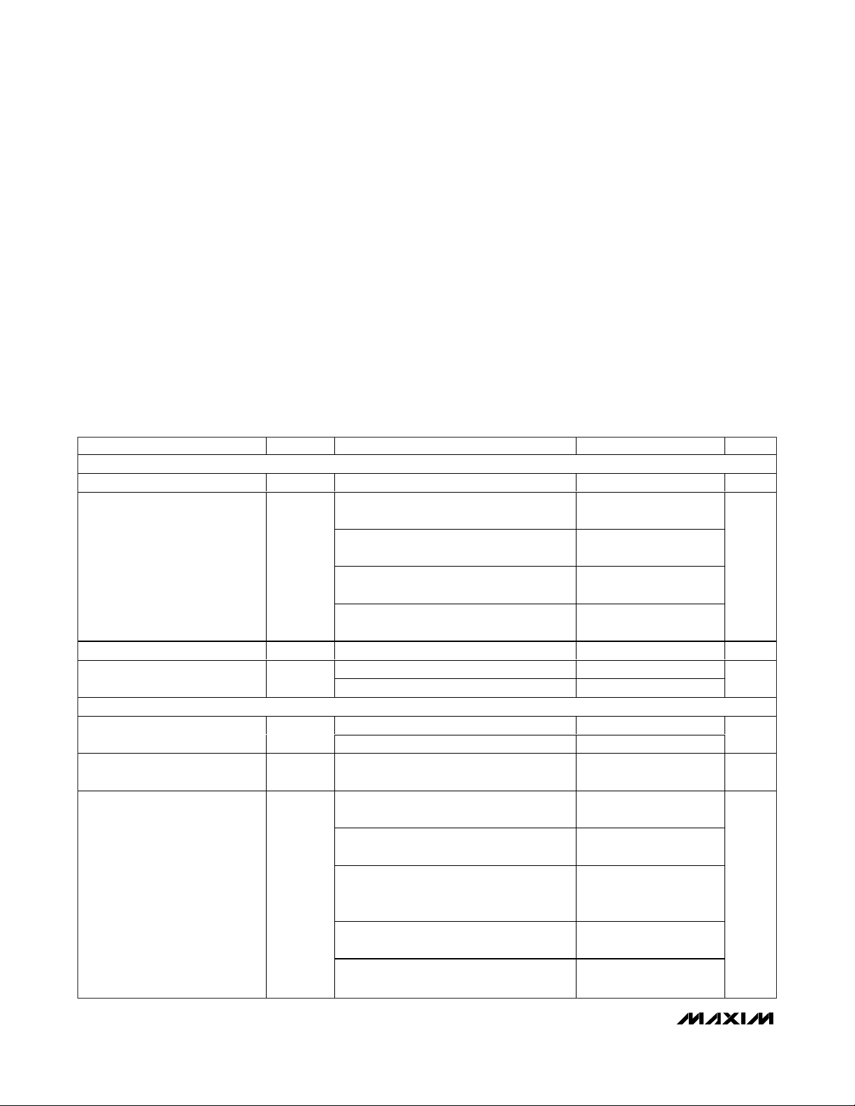
THIN QFN
TOP VIEW
LDO
DCIN
ACIN
REF
GND/PKPRES
ACOK
MODE
PDL
PDS
CSSP
CSSN
SRC
DHI
DHIV
DLOV
DLO
PGND
CSIP
CSIN
BATT
GND
CCS
CCV
CCI
VCTL
ICTL
CLS
IINP
Pin Configuration
CSSP CSSN
LDO
DHI
DLOV
DLO
PGND
CSIP
CSIN
BATT
GND
DCIN
VCTL
ICTL
MODE
ACIN
ACOK
CLS
CCV
CCI
CCS
REF
LDO
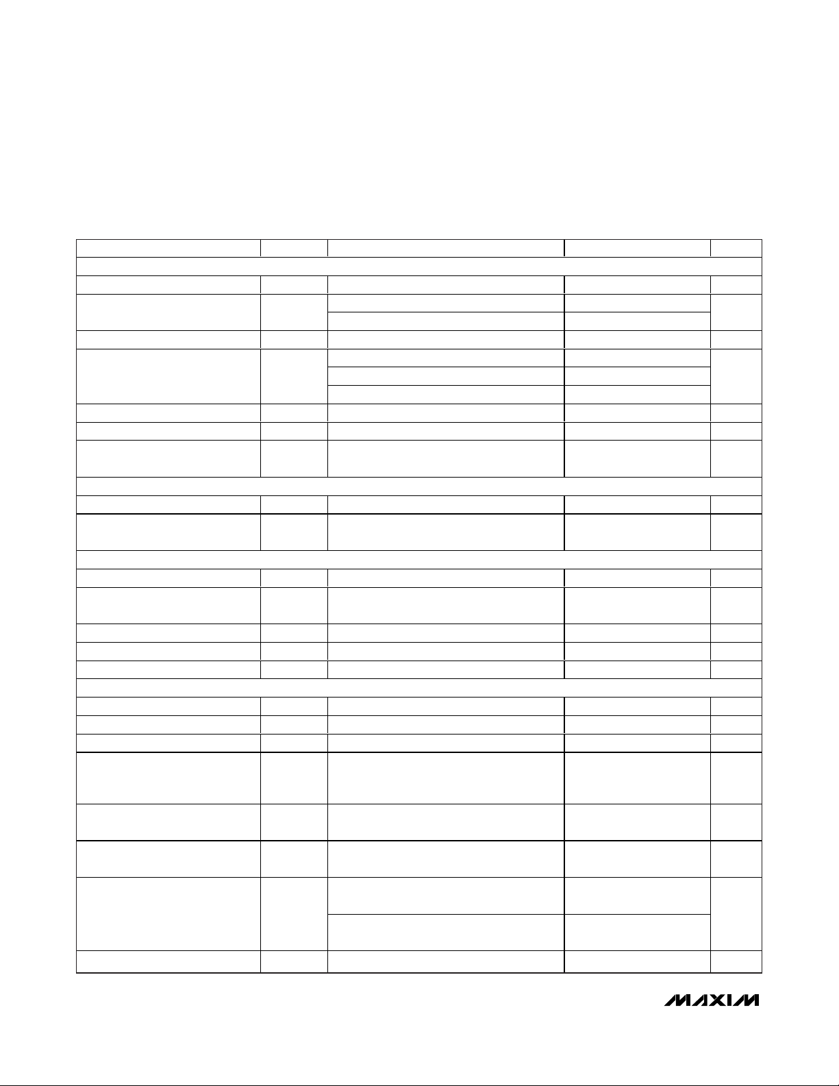
AC ADAPTER: INPUT
P3
0.01Ω
10μH
N1
P1
0.015Ω
TO
EXTERNAL LOAD
LDO
PDS
PDL
SRC
LDO
REF
IINP
IINP
DHIV
SRC
P2
MAX1909
MAX8725
PKPRES
MAX8725 ONLY
Minimum Operating Circuit
+
Denotes lead-free package.
Page 2
MAX1909/MAX8725
Multichemistry Battery Chargers with Automatic
System Power Selector
2 _______________________________________________________________________________________
ABSOLUTE MAXIMUM RATINGS
ELECTRICAL CHARACTERISTICS
(Circuit of Figure 1, V
DCIN
= V
CSSP
= V
CSSN
= 18V, V
BATT
= V
CSIP
= V
CSIN
= 12V, V
VCTL
= V
ICTL
= 1.8V, MODE = float, ACIN = 0, CLS =
REF, GND = PGND = 0, PKPRES = GND, LDO = DLOV, T
A
= 0°C to +85°C, unless otherwise noted. Typical values are at TA= +25°C.)
Stresses beyond those listed under “Absolute Maximum Ratings” may cause permanent damage to the device. These are stress ratings only, and functional
operation of the device at these or any other conditions beyond those indicated in the operational sections of the specifications is not implied. Exposure to
absolute maximum rating conditions for extended periods may affect device reliability.
DCIN, CSSP, CSSN, SRC, ACOK to GND..............-0.3V to +30V
DHIV ........................................................…SRC + 0.3, SRC - 6V
DHI, PDL, PDS to GND ...............................-0.3V to (V
SRC
+ 0.3)
BATT, CSIP, CSIN to GND .....................................-0.3V to +20V
CSIP to CSIN or CSSP to CSSN or PGND to GND ...-0.3V to +0.3V
CCI, CCS, CCV, DLO, IINP, REF,
ACIN to GND ........................................-0.3V to (V
LDO
+ 0.3V)
DLOV, VCTL, ICTL, MODE, CLS, LDO,
PKPRES to GND ...................................................-0.3V to +6V
DLOV to LDO.........................................................-0.3V to +0.3V
DLO to PGND ..........................................-0.3V to (DLOV + 0.3V)
LDO Short-Circuit Current...................................................50mA
Continuous Power Dissipation (T
A
= +70°C)
28-Pin TQFN (derate 20.8mW/°C above +70°C) .......1666mW
Operating Temperature Range ...........................-40°C to +85°C
Junction Temperature......................................................+150°C
Storage Temperature Range .............................-60°C to +150°C
Lead Temperature (soldering, 10s) .................................+300°C
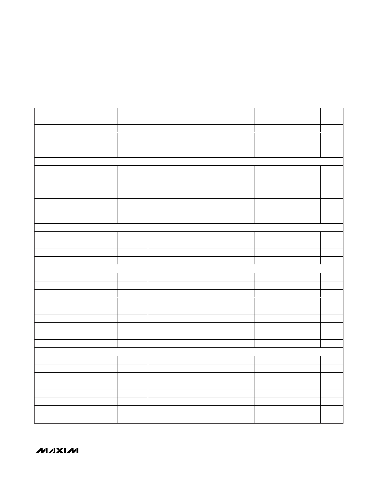
PARAMETER
SYMBOL
CONDITIONS
MIN
TYP
MAX
UNITS
CHARGE VOLTAGE REGULATION
VCTL Range 0 3.6 V
V
VCTL
= 3.6V (3 or 4 cells);
not including VCTL resistor tolerances
V
VCTL
= 3.6V/20 (3 or 4 cells); not including
VCTL resistor tolerances
V
VCTL
= 3.6V (3 or 4 cells); including VCTL
resistor tolerances of 1%
Battery Regulation Voltage
Accuracy
V
VCTL
= V
LDO
(3 or 4 cells, default
threshold of 4.2V/cell)
%
V
VCTL
Default Threshold V
VCTL
rising 4.1 4.3 V
V
VCTL
= 3V 0 2.5
VCTL Input Bias Current
V
DCIN
= 0, V
VCTL
= 5V 0 12
µA
CHARGE-CURRENT REGULATION
MAX1909 0 3.6
ICTL Range
MAX8725 0 3.2
V
CSIP-to-CSIN Full-Scale Current-
Sense Voltage
mV
MAX1909: V
ICTL
= 3.6V (not including ICTL
resistor tolerances)
MAX8725: V
ICTL
= 3.2V (not including ICTL
resistor tolerances)
-5 +5
MAX1909: V
ICTL
= 3.6V x 0.5, MAX8725:
V
ICTL
= 3.2V x 0.5 (not including ICTL
resistor tolerances)
-5 +5
MAX1909: V
ICTL
= 0.9V (not including ICTL
resistor tolerances)
Charge-Current Accuracy
MAX8725: V
ICTL
= 0.18V (not including
ICTL resistor tolerances)
-30
%
-0.8
-0.8
-1.0
-0.5
69.37 75.00 80.63
-7.5
-7.5
+0.8
+0.8
+1.0
+0.5
+7.5
+7.5
+30
Page 3
MAX1909/MAX8725
Multichemistry Battery Chargers with Automatic
System Power Selector
_______________________________________________________________________________________ 3
ELECTRICAL CHARACTERISTICS (continued)
(Circuit of Figure 1, V
DCIN
= V
CSSP
= V
CSSN
= 18V, V
BATT
= V
CSIP
= V
CSIN
= 12V, V
VCTL
= V
ICTL
= 1.8V, MODE = float, ACIN = 0, CLS =
REF, GND = PGND = 0, PKPRES = GND, LDO = DLOV, T
A
= 0°C to +85°C, unless otherwise noted. Typical values are at TA= +25°C.)
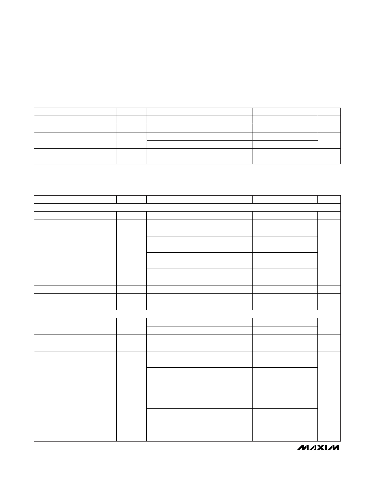
PARAMETER
SYMBOL
CONDITIONS
MIN
TYP
MAX
UNITS
MAX1909: V
ICTL
= 3.6V x 0.5, MAX8725:
V
ICTL
= 3.2V x 0.5 (including ICTL resistor
tolerances of 1%)
Charge-Current Accuracy
V
ICTL
= V
LDO (default threshold of 45mV)
-5 +5
%
V
ICTL
Default Threshold V
ICTL
rising 4.1 4.2 4.3 V
BATT/CSIP/CSIN Input Voltage
Range
0 19 V
Charging enabled
650
CSIP/CSIN Input Current
0.1 1
µA
MAX1909
ICTL Power-Down Mode
Threshold Voltage
MAX8725
V
MAX1909
ICTL Power-Up Mode Threshold
Voltage
MAX8725
V
V
ICTL
= 3V -1 +1
ICTL Input Bias Current
V
DCIN
= 0V, V
ICTL
= 5V
-1 +1
µA
INPUT CURRENT REGULATION
CSSP-to-CSSN Full-Scale
Current-Sense Voltage
mV
V
CLS
= REF -3 +3
V
CLS
= REF x 0.75 -3 +3
Input Current-Limit
Accuracy
V
CLS
= REF x 0.5 -4 +4
%
8.0 28 V
V
CSSP
= V
CSSN
= V
DCIN
> 8.0V
730
CSSP/CSSN Input Current
V
DCIN
= 0 0.1 1
µA
CLS Input Range 1.6
V
CLS Input Bias Current V
CLS
= 2.0V -1 +1 µA
IINP Transconductance V
CSSP
- V
CSSN
= 56mV 2.7 3.0 3.3
mA/V
V
CSSP
- V
CSSN
= 75mV, terminated with
10kΩ
V
CSSP
- V
CSSN
= 56mV, terminated with
10kΩ
-5 +5IINP Accuracy
V
CSSP
- V
CSSN
= 20mV, terminated with
10kΩ
-10
%
IINP Output Current V
CSSP
- V
CSSN
= 150mV, V
IINP
= 0V
µA
IINP Output Voltage V
CSSP
- V
CSSN
= 150mV, V
IINP
= float
3.5 V
C S S P /C S S N Inp ut V ol tag e Rang e
Charging disabled; V
DCIN
= 0 or V
ICTL
= 0
-7.0
+7.0
350
0.75
0.06
0.85
0.11
72.75 75.00 77.25
450
REF
-7.5
+7.5
+10
350
Page 4
MAX1909/MAX8725
Multichemistry Battery Chargers with Automatic
System Power Selector
4 _______________________________________________________________________________________
ELECTRICAL CHARACTERISTICS (continued)
(Circuit of Figure 1, V
DCIN
= V
CSSP
= V
CSSN
= 18V, V
BATT
= V
CSIP
= V
CSIN
= 12V, V
VCTL
= V
ICTL
= 1.8V, MODE = float, ACIN = 0, CLS =
REF, GND = PGND = 0, PKPRES = GND, LDO = DLOV, T
A
= 0°C to +85°C, unless otherwise noted. Typical values are at TA= +25°C.)
PARAMETER
SYMBOL
CONDITIONS
MIN
TYP
MAX
UNITS
SUPPLY AND LINEAR REGULATOR
DCIN Input Voltage Range V
DCIN
8.0 28 V
DCIN falling 7 7.4
DCIN Undervoltage-Lockout Trip
Point
DCIN rising 7.5
V
DCIN Quiescent Current I
DCIN
8.0V < V
DCIN
< 28V 2.7 6 mA
V
BATT
= 19V, V
DCIN
= 0V, or ICTL = 0V 0.1 1
V
BATT
= 16.8V, V
DCIN
= 19V, ICTL = 0V 0.1 1
BATT Input Current I
BATT
V
BATT
= 2V to 19V, V
DCIN
> V
BATT
+ 0.3V
500
µA
LDO Output Voltage 8.0V < V
DCIN
< 28V, no load
5.4
V
LDO Load Regulation 0 < I
LDO
< 10mA 80 115 mV
LDO Undervoltage-Lockout Trip
Point
V
DCIN
= 8.0V
4
V
REFERENCE
REF Output Voltage Ref 0 < I
REF
< 500µA
V
REF Undervoltage-Lockout Trip
Point
REF falling 3.1 3.9 V
TRIP POINTS
BATT POWER_FAIL Threshold V
DCIN
- V
BATT
, V
DCIN
falling 50
150 mV
BATT POWER_FAIL Threshold
Hysteresis
300 mV
ACIN Threshold ACIN rising
V
ACIN Threshold Hysteresis 10 20 30 mV
ACIN Input Bias Current V
ACIN
= 2.048V -1 +1 µA
SWITCHING REGULATOR
DHI Off-Time V
B AT T
= 16.0V , V
D C I N
= 19V , V
M OD E
= 3.6V
440 ns
DHI Minimum Off-Time V
B AT T
= 16.0V , V
D C I N
= 17V , V
M OD E
= 3.6V
350 ns
DLOV Supply Current I
DLOV
DLO low 5 10 µA
Sense Voltage for Minimum
Discontinuous Mode Ripple
Current
7.5 mV
Cycle-by-Cycle Current-Limit
Sense Voltage
97 mV
Sense Voltage for Battery
Undervoltage Charge Current
MAX1909 only, BATT = 3.0V per cell 3 4.5 6 mV
MAX1909 only, MODE = float (3 cell),
V
BATT
rising
Battery Undervoltage Threshold
MAX1909 only, MODE = LDO (4 cell),
V
BATT
rising
V
DHIV Output Voltage With respect to SRC
V
7.85
200
5.25
3.20
4.2023 4.2235 4.2447
100
100 200
2.007 2.048 2.089
360 400
260 300
9.18
12.235
-4.5 -5.0 -5.5
5.55
5.15
9.42
12.565
Page 5
MAX1909/MAX8725
Multichemistry Battery Chargers with Automatic
System Power Selector
_______________________________________________________________________________________ 5
ELECTRICAL CHARACTERISTICS (continued)
(Circuit of Figure 1, V
DCIN
= V
CSSP
= V
CSSN
= 18V, V
BATT
= V
CSIP
= V
CSIN
= 12V, V
VCTL
= V
ICTL
= 1.8V, MODE = float, ACIN = 0, CLS =
REF, GND = PGND = 0, PKPRES = GND, LDO = DLOV, T
A
= 0°C to +85°C, unless otherwise noted. Typical values are at TA= +25°C.)
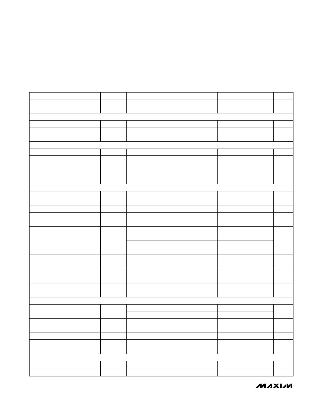
PARAMETER
SYMBOL
CONDITIONS
MIN
TYP
MAX
UNITS
DHIV Sink Current 10 mA
DHI On-Resistance Low DHI = V
DHIV
, I
DHI
= -10mA 2 5 Ω
DHI On-Resistance High DHI = V
CSSN
, I
DHI
= 10mA 2 4 Ω
DLO On-Resistance High V
DLOV
= 4.5V, I
DLO
= +100mA 3 7 Ω
DLO On-Resistance Low V
DLOV
= 4.5V, I
DLO
= -100mA 1 3 Ω
ERROR AMPLIFIERS
V C TL = 3.6, V
BATT
= 16.8V , M OD E = LD O
GMV Loop Transconductance
V C TL = 3.6, V
BATT
= 12.6V , M OD E = FLOAT
mA/V
GMI Loop Transconductance
MAX1909: ICTL = 3.6V, MAX8725: V
ICTL
=
3.2V, V
CSSP
- V
CSIN
= 75mV
0.5 1 2
mA/V
GMS Loop Transconductance V
CLS
= 2.048V, V
CSSP
- V
CSSN
= 75mV 0.5 1 2
mA/V
CCI/CCS/CCV Clamp Voltage
0.25V < V
CCS
< 2.0V
600 mV
LOGIC LEVELS
MODE Input Low Voltage 0.8 V
MODE Input Middle Voltage 1.6 1.8 2.0 V
MODE Input High Voltage 2.8 V
MODE Input Bias Current MODE = 0V or 3.6V -2 +2 µA
ACOK AND PKPRES
ACOK Input Voltage Range 0 28 V
ACOK Sink Current V
ACOK
= 0.4V, ACIN = 1.5V 1 mA
ACOK Leakage Current V
ACOK
= 28V, ACIN = 2.5V 1 µA
PKPRES Input Voltage
Range
0
V
PKPRES Input Bias Current -1 +1 µA
PKPRES Battery Removal Detect
Threshold
MAX8725, PKPRES rising 55
% of
LDO
PKPRES Hysteresis MAX8725 1 %
PDS, PDL SWITCH CONTROL
PDS Switch Turn-Off Threshold V
DCIN
- V
BATT
, V
DCIN
falling 50
150 mV
V
DCIN
- V
BATT
300 mV
PDS Output Low Voltage, PDS
Below SRC
I
PDS
= 0A 8 10 12 V
PDS Turn-On Current PDS = SRC 6 12 mA
PDS Turn-Off Current V
PDS
= V
SRC
- 2V, V
DCIN
= 16V 10 50 mA
PDL Switch Turn-On Threshold V
DCIN
- V
BATT
, V
DCIN
falling 50
150 mV
V
DCIN
- V
BATT
300 mV
0.0625 0.125 0.2500
0.0833 0.167 0.3330
0.25V < V
< 2.0V, 0.25V < V
CCV
< 2.0V,
CCI
150 300
PDS Switch Threshold Hysteresis
100 200
100
PDL Switch Threshold Hysteresis
100 200
100
LDO
Page 6
MAX1909/MAX8725
Multichemistry Battery Chargers with Automatic
System Power Selector
6 _______________________________________________________________________________________
ELECTRICAL CHARACTERISTICS
(Circuit of Figure 1, V
DCIN
= V
CSSP
= V
CSSN
= 18V, V
BATT
= V
CSIP
= V
CSIN
= 12V, V
VCTL
= V
ICTL
= 1.8V, MODE = float, ACIN = 0, CLS =
REF, GND = PGND = 0, PKPRES = GND, LDO = DLOV, T
A
= -40°C to +85°C, unless otherwise noted.)
PARAMETER
SYMBOL
CONDITIONS
MIN
TYP
MAX
UNITS
CHARGE VOLTAGE REGULATION
VCTL Range 0 3.6 V
V
VCTL
= 3.6V (3 or 4 cells); not including
VCTL resistor tolerances
V
VCTL
= 3.6V/20 (3 or 4 cells); not including
VCTL resistor tolerances
V
VCTL
= 3.6V (3 or 4 cells); including VCTL
resistor tolerances of 1%
Battery Regulation Voltage
Accuracy
V
VCTL
= V
LDO
(3 or 4 cells, default
threshold of 4.2V/cell)
%
V
VCTL
Default Threshold V
VCTL
rising 4.1 4.3 V
V
VCTL
= 3V 0 2.5
VCTL Input Bias Current
V
DCIN
= 0V, V
VCTL
= 5V
0 12
µA
CHARGE-CURRENT REGULATION
MAX1909 0 3.6
ICTL Range
MAX8725 0 3.2
V
CSIP-to-CSIN Full-Scale Current-
Sense Voltage
mV
MAX1909: V
ICTL
= 3.6V (not including ICTL
resistor tolerances)
MAX8725: V
ICTL
= 3.2V (not including ICTL
resistor tolerances)
-5 +5
MAX1909: V
ICTL
= 3.6V x 0.5, MAX8725:
V
ICTL
= 3.2V x 0.5 (not including ICTL
resistor tolerances)
-5 +5
MAX1909: V
ICTL
= 0.9V (not including ICTL
resistor tolerances)
Charge-Current Accuracy
MAX8725: V
ICTL
= 0.18V (not including
ICTL resistor tolerances)
-30
%
ELECTRICAL CHARACTERISTICS (continued)
(Circuit of Figure 1, V
DCIN
= V
CSSP
= V
CSSN
= 18V, V
BATT
= V
CSIP
= V
CSIN
= 12V, V
VCTL
= V
ICTL
= 1.8V, MODE = float, ACIN = 0, CLS =
REF, GND = PGND = 0, PKPRES = GND, LDO = DLOV, T
A
= 0°C to +85°C, unless otherwise noted. Typical values are at TA= +25°C.)
PARAMETER
SYMBOL
CONDITIONS
MIN
TYP
MAX
UNITS
PDL Turn-On Resistance PDL = GND 50
150 kΩ
PDL Turn-Off Current V
SRC
- V
PDL
= 1.5V 6 12 mA
SRC = 19V, DCIN = 0V 1
SRC Input Bias Current
SRC = 19, V
BATT
= 16V
µA
Delay Time Between PDL and
PDS Transitions
2.5 5 7.5 µs
100
450 1000
-0.8
-0.8
-1.0
-0.8
69.37
-7.5
-7.5
+0.8
+0.8
+1.0
+0.8
80.63
+7.5
+7.5
+30
Page 7
MAX1909/MAX8725
Multichemistry Battery Chargers with Automatic
System Power Selector
_______________________________________________________________________________________ 7
ELECTRICAL CHARACTERISTICS (continued)
(Circuit of Figure 1, V
DCIN
= V
CSSP
= V
CSSN
= 18V, V
BATT
= V
CSIP
= V
CSIN
= 12V, V
VCTL
= V
ICTL
= 1.8V, MODE = float, ACIN = 0, CLS =
REF, GND = PGND = 0, PKPRES = GND, LDO = DLOV, T
A
= -40°C to +85°C, unless otherwise noted.)
PARAMETER
SYMBOL
CONDITIONS
MIN
TYP
MAX
UNITS
MAX1909: V
ICTL
= 3.6V x 0.5, MAX8725:
V
ICTL
= 3.2V x 0.5 (including ICTL resistor
tolerances of 1%)
Charge-Current Accuracy
V
ICTL
= V
LDO (default threshold of 45mV)
-5 +5
%
V
ICTL
Default Threshold V
ICTL
rising 4.3 V
BATT/CSIP/CSIN Input Voltage
Range
0 19 V
CSIP/CSIN Input Current Charging enabled 650 µA
MAX1909
ICTL Power-Down Mode
Threshold Voltage
MAX8725
V
MAX1909
ICTL Power-Up Mode Threshold
Voltage
MAX8725
V
INPUT CURRENT REGULATION
CSSP-to-CSSN Full-Scale
Current-Sense Voltage
mV
V
CLS
= REF -3 +3
V
CLS
= REF x 0.75 -3 +3Input Current-Limit Accuracy
V
CLS
= REF x 0.5 -4 +4
%
8.0 28 V
CSSP/CSSN Input Current V
CSSP
= V
CSSN
= V
DCIN
> 8.0V 730 µA
CLS Input Range 1.6
V
IINP Transconductance V
CSSP
- V
CSSN
= 56mV 2.7 3.3
mA/V
V
CSSP
- V
CSSN
= 75mV, terminated with
10kΩ
V
CSSP
- V
CSSN
= 56mV, terminated with
10kΩ
-5 +5IINP Accuracy
V
CSSP
- V
CSSN
= 20mV, terminated with
10kΩ
-10
%
IINP Output Current V
CSSP
- V
CSSN
= 150mV, V
IINP
= 0V
µA
IINP Output Voltage V
CSSP
- V
CSSN
= 150mV, V
IINP
= float
3.5 V
SUPPLY AND LINEAR REGULATOR
DCIN Input Voltage Range V
DCIN
8.0 28 V
DCIN falling 7
D C IN U nd er vol tag e- Lockout Tr i p
P oi nt
DCIN rising
V
DCIN Quiescent Current I
DCIN
8.0V < V
DCIN
< 28V 6 mA
BATT Input Current I
BATT
V
BATT
= 2V to 19V, V
DCIN
> V
BATT
+ 0.3V 500 µA
LDO Output Voltage 8.0V < V
DCIN
< 28V, no load
V
LDO Load Regulation 0 < I
LDO
< 10mA 115 mV
-7.0
CSSP/CSSN Input Voltage Range
0.85
0.11
72.75
-7.5
350
5.25
+7.0
0.75
0.06
77.25
REF
+7.5
+10
7.85
5.55
Page 8
MAX1909/MAX8725
Multichemistry Battery Chargers with Automatic
System Power Selector
8 _______________________________________________________________________________________
ELECTRICAL CHARACTERISTICS (continued)
(Circuit of Figure 1, V
DCIN
= V
CSSP
= V
CSSN
= 18V, V
BATT
= V
CSIP
= V
CSIN
= 12V, V
VCTL
= V
ICTL
= 1.8V, MODE = float, ACIN = 0, CLS =
REF, GND = PGND = 0, PKPRES = GND, LDO = DLOV, T
A
= -40°C to +85°C, unless otherwise noted.)
PARAMETER
SYMBOL
CONDITIONS
MIN
TYP
MAX
UNITS
LDO Undervoltage-Lockout Trip
Point
V
DCIN
= 8.0V
V
REFERENCE
REF Output Voltage Ref 0 < I
REF
< 500µA
V
REF Undervoltage-Lockout Trip
Point
REF falling 3.9 V
TRIP POINTS
BATT POWER_FAIL Threshold V
DCIN
- V
BATT
, V
DCIN
falling 50 150 mV
BATT POWER_FAIL Threshold
Hysteresis
300 mV
ACIN Threshold ACIN rising
V
ACIN Threshold Hysteresis 10 30 mV
SWITCHING REGULATOR
DHI Off-Time
440 ns
DHI Minimum Off-Time
350 ns
DLOV Supply Current I
DLOV
DLO low 10 µA
Sense Voltage for Battery
Undervoltage Charge Current
MAX1909 only, BATT = 3.0V per cell 3 6 mV
MAX1909 only, MODE = float (3 cell),
V
BATT
rising
Battery Undervoltage Threshold
MAX1909 only, MODE = LDO (4 cell),
V
BATT
rising
V
DHIV Output Voltage With respect to SRC
V
DHIV Sink Current 10 mA
DHI On-Resistance Low DHI = V
DHIV
, I
DHI
= -10mA 5 Ω
DHI On-Resistance High DHI = V
CSSN
, I
DHI
= 10mA 4 Ω
DLO On-Resistance High V
DLOV
= 4.5V, I
DLO
= +100mA 7 Ω
DLO On-Resistance Low V
DLOV
= 4.5V, I
DLO
= -100mA 3 Ω
ERROR AMPLIFIERS
V C TL = 3.6, V
BATT
= 16.8V , M OD E = LD O
GMV Loop Transconductance
V C TL = 3.6, V
BATT
= 12.6V , M OD E = FLOAT
mA/V
GMI Loop Transconductance
MAX1909: ICTL = 3.6V, MAX8725: V
ICTL
=
3.2V, V
CSSP
- V
CSIN
= 75mV
0.5 2.0
mA/V
GMS Loop Transconductance V
CLS
= 2.048V, V
CSSP
- V
CSSN
= 75mV 0.5 2.0
mA/V
CCI/CCS/CCV Clamp Voltage
0.25V < V
CCV
< 2.0V, 0.25V < V
CCI
< 2.0V,
0.25V < V
CCS
< 2.0V
600 mV
LOGIC LEVELS
MODE Input Low Voltage 0.8 V
MODE Input Middle Voltage 1.6 2.0 V
3.20
4.1960
V
V
100
2.007
= 16.0V, V
BATT
= 16.0V, V
BATT
DCIN
DCIN
= 19V, V
= 17V, V
= 3.6V 360
MODE
= 3.6V 260
MODE
9.18
12.235
-4.5
0.0625
0.0833
150
5.15
4.2520
2.089
9.42
12.565
-5.5
0.2500
0.3330
Page 9
MAX1909/MAX8725
Multichemistry Battery Chargers with Automatic
System Power Selector
_______________________________________________________________________________________ 9
ELECTRICAL CHARACTERISTICS (continued)
(Circuit of Figure 1, V
DCIN
= V
CSSP
= V
CSSN
= 18V, V
BATT
= V
CSIP
= V
CSIN
= 12V, V
VCTL
= V
ICTL
= 1.8V, MODE = float, ACIN = 0, CLS =
REF, GND = PGND = 0, PKPRES = GND, LDO = DLOV, T
A
= -40°C to +85°C, unless otherwise noted.)
PARAMETER
CONDITIONS
UNITS
MODE Input High Voltage 2.8 V
ACOK AND PKPRES
ACOK Input Voltage Range 0 28 V
ACOK Sink Current V
ACOK
= 0.4V, ACIN = 1.5V 1 mA
PKPRES Input Voltage Range 0
V
PKPRES Battery Removal Detect
Threshold
MAX8725, PKPRES rising 55
% of
LDO
PDS, PDL SWITCH CONTROL
PDS Switch Turn-Off Threshold V
DCIN
- V
BATT
, V
DCIN
falling 50 150 mV
P D S S w i tch Thr eshol d H yste r esi s V
DCIN
- V
BATT
300 mV
PDS Output Low Voltage, PDS
Below SRC
I
PDS
= 0A 8 12 V
PDS Turn-On Current PDS = SRC 6 mA
PDS Turn-Off Current V
PDS
= V
SRC
- 2V, V
DCIN
= 16V 10 mA
PDL Switch Turn-On Threshold V
DCIN
- V
BATT
, V
DCIN
falling 50 150 mV
P D L S w i tch Thr eshol d H yster esi s V
DCIN
- V
BATT
300 mV
PDL Turn-On Resistance PDL = GND 50 150 kΩ
PDL Turn-Off Current V
SRC
- V
PDL
= 1.5V 6 mA
SRC Input Bias Current SRC = 19, V
BATT
= 16V
µA
Note 1: Guaranteed by design. Not production tested.
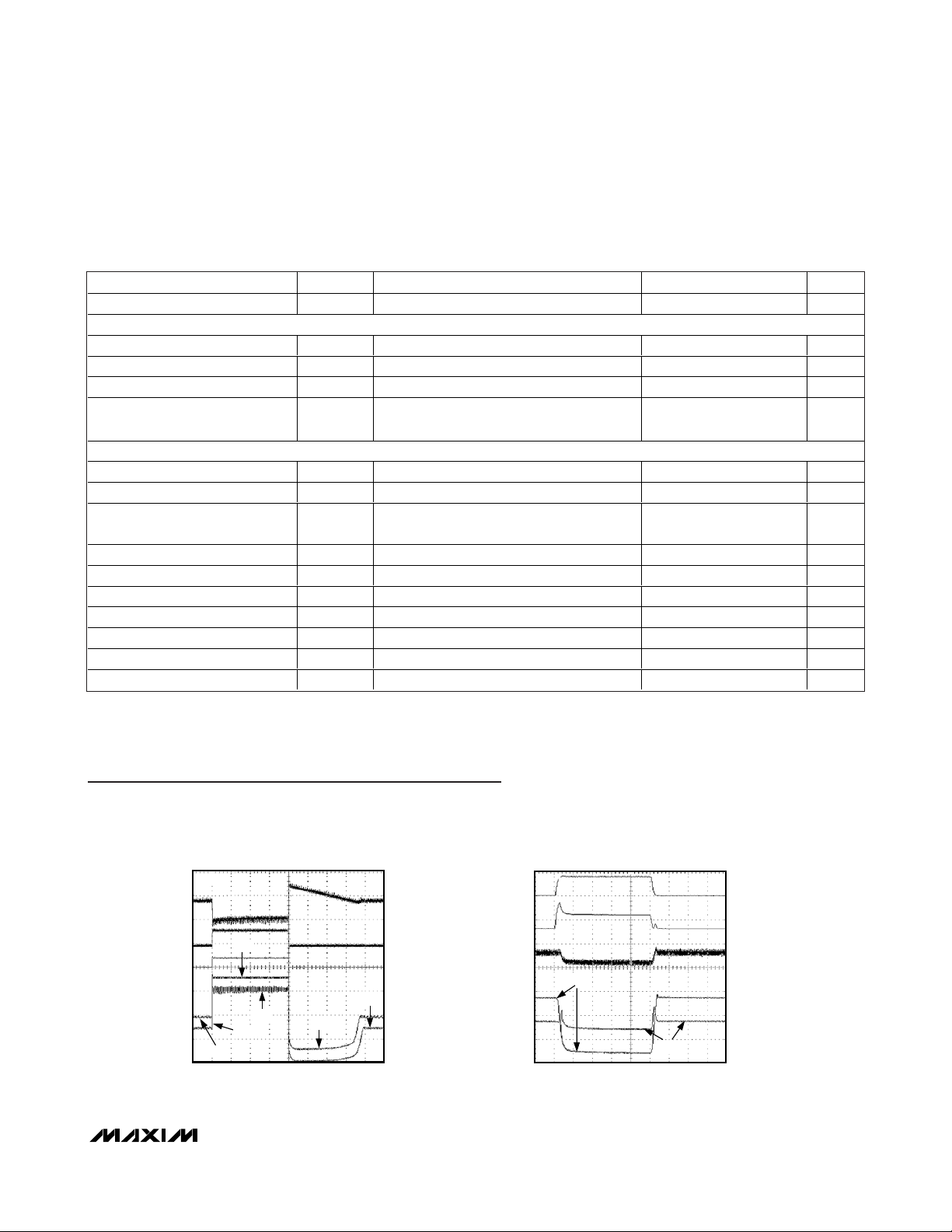
BATTERY INSERTION
AND REMOVAL RESPONSE
MAX1909/MAX8725 toc01
500μs/div
1V
0V
2V
3V
16V
17V
0A
0A
I
IN
I
BATT
V
BATT
V
CCI
, V
CCV
5A/div
5A/div
V
CCI
V
CCV
V
CCV
V
CCV
V
CCI
V
CCI
SYSTEM LOAD-TRANSIENT RESPONSE
MAX1909/MAX8725 toc02
100μs/div
1V
0V
2V
3V
5A
5A
0A
5A
0A
0A
I
BATT
I
IN
I
SYSTEMLOAD
V
CCS
V
CCI
CCS
CCI
Typical Operating Characteristics
(Circuit of Figure 2, V
DCIN
= 20V, charge current = 3A, 4 Li+ series cells, TA= +25°C, unless otherwise noted.)
SYMBOL
MIN TYP MAX
100
100
LDO
1000
Page 10

MAX1909/MAX8725
Multichemistry Battery Chargers with Automatic
System Power Selector
10 ______________________________________________________________________________________
LDO LOAD REGULATION
MAX1909/MAX8725 toc04
LDO CURRENT (mA)
LDO OUTPUT ERROR (%)
987654321
-1.2
-1.0
-0.8
-0.6
-0.4
-0.2
0
-1.4
010
LINE-TRANSIENT RESPONSE
MAX1909/MAX8725 toc03
500μs/div
1.8V
V
BATT
AC-COUPLED
200mV/div
INDUCTOR CURRENT
200mA/div
1.6V
3A
20V
30V
V
DCIN
V
CCV
REF vs. TEMPERATURE
MAX1909/MAX8725 toc07
TEMPERATURE (°C)
REF OUTPUT ERROR (%)
603510-15
-0.15
-0.10
-0.05
0
0.05
0.10
-0.20
-40 85
EFFICIENCY vs. CHARGE CURRENT
MAX1909/MAX8725 toc08
CHARGE CURRENT (A)
EFFICIENCY (%)
2.52.01.51.00.5
82
84
86
88
90
92
94
96
98
100
80
03.0
4 CELLS
3 CELLS
LDO LINE REGULATION
MAX1909/MAX8725 toc05
INPUT VOLTAGE (V)
LDO OUTPUT ERROR (%)
2010
-0.05
0
0.05
0.10
-0.10
030
REF LOAD REGULATION
MAX1909/MAX8725 toc06
REF CURRENT (μA)
REF OUTPUT ERROR (%)
800600400200
-0.12
-0.10
-0.08
-0.06
-0.04
-0.02
0
-0.14
0 1000
Typical Operating Characteristics (continued)
(Circuit of Figure 2, V
DCIN
= 20V, charge current = 3A, 4 Li+ series cells, TA= +25°C, unless otherwise noted.)
Page 11

MAX1909/MAX8725
Multichemistry Battery Chargers with Automatic
System Power Selector
______________________________________________________________________________________
11
SWITCHING FREQUENCY vs. VIN - V
BATT
MAX1909/MAX8725 toc09
VIN - V
BATT
(V)
SWITCHING FREQUENCY (kHz)
8642
50
100
150
200
250
300
350
400
450
500
0
010
IINP ERROR vs. INPUT CURRENT
MAX1909/MAX8725 toc10
INPUT CURRENT (A)
IINP (%)
3.02.50.5 1.0 1.5 2.0
0.5
1.0
1.5
2.0
2.5
3.0
3.5
4.0
0
03.5
CHARGER
DISABLED
-3
-1
-2
1
0
2
3
1.5 2.52.0 3.0 3.5
INPUT CURRENT-LIMIT ACCURACY vs. V
CLS
MAX1909/MAX8725 toc14
V
CLS
(V)
INPUT CURRENT-LIMIT ACCURACY (%)
-8
-4
-6
2
0
-2
6
4
8
1.5 3.0 3.52.0 2.5 4.0 4.5 5.0 5.5 6.0
IINP ACCURACY vs. INPUT CURRENT
MAX1909/MAX8725 toc11
INPUT CURRENT (A)
IINP ACCURACY (%)
-2
0
-1
2
1
3
4
0.5 1.51.0 2.0 2.5 3.0
INPUT CURRENT-LIMIT ACCURACY
vs. SYSTEM LOAD
MAX1909/MAX8725 toc12
SYSTEM LOAD (A)
INPUT CURRENT-LIMIT ACCURACY (%)
V
BATT
= 10V
V
BATT
= 13V
V
BATT
= 12V
V
BATT
= 16V
I
CHARGE
= 3A
MAX1909 ONLY
Typical Operating Characteristics (continued)
(Circuit of Figure 2, V
DCIN
= 20V, charge current = 3A, 4 Li+ series cells, TA= +25°C, unless otherwise noted.)
INPUT CURRENT-LIMIT ACCURACY
vs. SYSTEM LOAD
MAX1909/MAX8725 toc13
SYSTEM LOAD (A)
INPUT CURRENT-LIMIT ACCURACY (%)
3.02.50.5 1.0 1.5 2.0
-1
0
1
2
3
4
-2
03.5
V
BATT
= 16V V
BATT
= 12V
V
BATT
= 13V
V
BATT
= 10V
Page 12

MAX1909/MAX8725
Multichemistry Battery Chargers with Automatic
System Power Selector
12 ______________________________________________________________________________________
Typical Operating Characteristics (continued)
(Circuit of Figure 2, V
DCIN
= 20V, charge current = 3A, 4 Li+ series cells, TA= +25°C, unless otherwise noted.)
PDL-PDS SWITCHING,
AC ADAPTER INSERTION
MAX1909/MAX8725 toc15
100μs/div
10V
20V
10V
20V
10V
20V
0V
V
WALLADAPTER
V
SYSTEMLOAD
, V
PDS
V
PDS
V
PDL
, V
BATT
V
PDL
SYSTEM LOAD
V
PDL
V
PDS
PDS-PDL SWITCHOVER,
WALL ADAPTER REMOVAL
MAX1909/MAX8725 toc16
500μs/div
10V
20V
0V
10V
20V
10V
20V
0V
V
WALLADAPTER
V
SYSTEMLOAD
V
SYSTEMLOAD
V
PDS
V
PDL
V
BATT
V
PDL
PDS-PDL SWITCHOVER,
BATTERY INSERTION
MAX1909/MAX8725 toc17
50μs/div
10V
15V
0V
5V
10V
15V
20V
5V
0V
V
SYSTEM
V
PDS
V
PDL
V
BATT
V
PKDET
CONDITIONING MODE
WALL ADAPTER = 18V
V
PKPRES
PDL-PDS SWITCHING,
BATTERY REMOVAL
MAX1909/MAX8725 toc18
10μs/div
10V
15V
0V
5V
10V
15V
20V
5V
0V
V
SYSTEM
V
PDS
V
PDL
V
BATT
CONDITIONING MODE
WALL ADAPTER = 18V
V
PKPRES
MAX8725 ONLY
Page 13

MAX1909/MAX8725
Pin Description
PIN NAME FUNCTION
1 DCIN DC Supply Voltage Input. Bypa ss DCIN with a 1μF capacitor to power ground.
2 LDO Device Power Supply. Output of the 5.4V linear regulator supplied from DCIN. Bypass with a 1μF capacitor.
3 ACIN
AC Detect Input. This uncommitted comparator input can be used to detect the presence of the charger’s
power source. The comparator’s open-drain output i s the ACOK signal.
4 REF 4.2235V Voltage Reference. Bypass with a 1μF capacitor to GND.
GND MAX1909: Ground thi s pin.
5
PKPRES MAX8725: Pull PKPRES high to disable charging. Used for detecting presence of battery pac k.
6 ACOK
AC Detect Output. High-voltage open-drain output is high impedance when ACIN is greater than 2.048V.
The ACOK output remains a high impedance when the MAX1909/MAX8725 are powered down.
7 MODE
Trilevel Input for Setting Number of Cells and Asserting the Conditioning Mode:
MODE = GND; asserts conditioning mode.
MODE = float; charge with 3 times the cell vo ltage programmed at VCTL.
MODE = LDO; charge with 4 times the cell voltage programmed at VCTL.
8 IINP
Input Current Mon itor Output. The current delivered at the IINP output is a scaled-down replica of the
sy stem load current plus the input-referred charge current sensed across CSSP and CSSN inputs. The
transconductance of (CSSP - CSSN) to IINP is 3mA/V.
9 CLS Source Current-Limit Input. Voltage input for setting the current limit of the input source.
10 ICTL Input for Setting Maximum Output Current
11 VCTL Input for Setting Ma ximum Output Voltage
12 CCI Output Current-Regulation Loop-Compensat ion Point. Connect 0.01μF to GND.
13 CCV Voltage-Regulation Loop-Compensation Point. Connect 10k in series with 0.1μF to GND.
14 CCS Input Current-Regulat ion Loop-Compensation Point. Use 0.01μF to GND.
15 GND Analog Ground
16 BATT Battery Voltage Feedback Input
17 CSIN Output Current-Sense Negative Input
18 CSIP Output Current-Sense Positive Input. Connect a current-sense resistor from CSIP to CSIN.
19 PGND Power Ground
20 DLO
Low-Side Power-MOSFET Driver Output. Connect to low-side NMOS gate. When the MAX1909/MAX8725 are
shut down, the DLO output is low.
21 DLOV Low-Side Driver Supply. Bypas s w ith a 1μF capacitor to ground.
22 DHIV High-Side Dri ver Supply. Bypass with a 0.1μF capacitor to SRC.
23 DHI
High-Side Power-MOSFET Driver Output. Connect to high-side PMOS gate. When the MAX1909/MAX8725
are shut down, the DHI output i s
high.
24 SRC Source Connection for Driver for PDS/PDL Switches. Bypass SRC to power ground with a 1μF capacitor.
25 CSSN Input Current Sense for Charger (Negative Input)
26 CSSP Input Current Sense for Charger (Positive Input). Connect a current-sen se resistor from CSSP to CSSN.
27 PDS
Power-Source PMOS Switch Dri ver Output. When the MAX1909/MAX8725 are powered down, the PDS output
is pulled to SRC through an internal 1M resistor.
28 PDL
System-Load PMOS Switch Driver Output. When the MAX1909/MAX8725 are powered down, the PDL output
is p ul led to ground through an internal 100k resistor.
Multichemistry Battery Chargers with Automatic
System Power Selector
______________________________________________________________________________________ 13
Page 14

MAX1909/MAX8725
Multichemistry Battery Chargers with Automatic
System Power Selector
14 ______________________________________________________________________________________
CSSP CSSN
LDO
DHI
DLOV
DLO
PGND
CSIP
CSIN
BATT
GND
DCIN
VCTL
ICTL
MODE
ACIN
ACOK
CLS
CCV
CCI
CCS
REF
GND
TO
HOST
SYSTEM
BATT +
TEMP
BATT -
BATTERY
AC ADAPTER
R6
590kΩ
1%
R7
196kΩ
1%
C5
1μF
D4
P3
RS1
0.01Ω
R5
10kΩ
C11
0.1μF
C10
0.01μF
C9
0.01μF
C12
1μF
C4
22μF
N1
P1
C16
1μF
C13
1μF
R13
33Ω
C1
22μF
GND
PGND
RS2
0.015Ω
TO
SYSTEM LOAD
R8
1M
Ω
LDO
OUTPUT
(INPUT I LIMIT: 7.5A)
OUTPUT VOLTAGE: 12.6V
CHARGE I LIMIT: 3.0A
PDS
PDL
SRC
LDO
REF
DHIV
C17
0.1μF
R4
100kΩ
SRC
C22
1μF
R9
10kΩ
P2
MAX1909
MAX8725
PKPRES (MAX8725 ONLY)
L1
10μH
LDO
LDO
0.1μF
0.1μF
Figure 1. Typical Operating Circuit Demonstrating Hardwired Control
Page 15

MAX1909/MAX8725
Multichemistry Battery Chargers with Automatic
System Power Selector
______________________________________________________________________________________ 15
CSSP CSSN
LDO
DHI
DLOV
DLO
PGND
CSIP
CSIN
BATT
GND
DCIN
VCTL
ICTL
ACIN
MODE
ACOK
IINP
CCV
CCI
CCS
REF
AV
DD
/REF
SCL
SDA
GND
HOST
BATT +
TEMP
SDA
SCL
BATT -
SMART
BATTERY
AC ADAPTER
R6
590kΩ
1%
R7
196kΩ
1%
C5
1μF
D4
P3 P4
RS1
0.01Ω
R5
10kΩ
C11
0.1μF
C10
0.01μF
C9
0.01μF
C12
1μF
C4
22μF
N1
P1
C16
1μF
C13
1μF
R13
33Ω
C1
22μF
GND
PGND
RS2
0.015Ω
TO
SYSTEM LOAD
R8
1MΩ
LDO
OUTPUTS
OUTPUT
INPUT
A/D INPUT
OPEN-DRAIN
OUTPUT VOLTAGE: 16.8V
PDS
PDL
SRC
LDO
CLSREF
DHIV
C17
0.1μF
SRC
C15
1μF
R21
10kΩ
P2
MAX1909
MAX8725
C14
0.1μF
R9
10kΩ
R19, R20
10kΩ
(INPUT I LIMIT: 7.5A)
L1
10μH
D/A OUTPUT
0.1μF
0.1μF
LDO
PKPRES (MAX8725 ONLY)
Figure 2. Smart-Battery Charger Circuit Demonstrating Operation with a Host Microcontroller
Page 16

MAX1909/MAX8725
Multichemistry Battery Chargers with Automatic
System Power Selector
16 ______________________________________________________________________________________
CHG
LOGIC
5.4V
LINEAR
REGULATOR
4.2235V
REFERENCE
LDO
DCIN
REF
ACOK
2.048V
IINP
DC-DC
CONVERTER
PDS
DHI
PDL
DRIVER
DRIVER
DRIVER
DRIVER
DLOV
DLO
PGND
LVC
BATT
MODE
VCTL
CSIP
CSIN
LEVEL
SHIFTER
LEVEL
SHIFTER
CSSP
CSSN
ICTL
CLS
SRDY
GND
GND
GMV
GMI
GMS
CCS
CCI
CCV
CELL SELECT
LOGIC AND
BATTERY VOLTAGE-
DIVIDER
ACIN
0.9 * LDO
RDY
SRC
SWITCH LOGIC
R
R
9R
REF
MODE
DHIV
DCIN
0.8V
Gm
BATT
PKPRES
3.0V/CELL
BATT_UV
ICTLOK
PACK_ON
CHG
SRC
MAX1909
MAX8725
SRC-10V
100k
Ω
MAX1909 ONLY
MAX8725 ONLY
Figure 3. Functional Diagram
Page 17

MAX1909/MAX8725
Multichemistry Battery Chargers with Automatic
System Power Selector
______________________________________________________________________________________ 17
Detailed Description
The MAX1909/MAX8725 include all of the functions
necessary to charge Li+, NiMH, and NiCd batteries. A
high-efficiency, synchronous-rectified step-down DCDC converter is used to implement a precision constant-current, constant-voltage charger with input
current limiting. The DC-DC converter uses external
p-channel/n-channel MOSFETs as the buck switch and
synchronous rectifier to convert the input voltage to the
required charge current and voltage. The charge current and input current-limit sense amplifiers have lowinput-referred offset errors and can use small-value
sense resistors. The MAX1909/MAX8725 feature a voltage-regulation loop (CCV) and two current-regulation
loops (CCI and CCS). The CCV voltage-regulation loop
monitors BATT to ensure that its voltage never exceeds
the voltage set by VCTL. The CCI battery current-regulation loop monitors current delivered to BATT to ensure
that it never exceeds the current limit set by ICTL. A
third loop (CCS) takes control and reduces the charge
current when the sum of the system load and the inputreferred charge current exceeds the power source current limit set by CLS. Tying CLS to the reference
voltage provides a 7.5A input current limit with a 10mΩ
sense resistor.
The ICTL, VCTL, and CLS analog inputs set the charge
current, charge voltage, and input current limit, respectively. For standard applications, internal set points for
ICTL and VCTL provide a 3A charge current using a
15mΩ sense resistor and a 4.2V per-cell charge voltage. The variable for controlling the number of cells is
set with the MODE input. The MAX8725 includes a
PKPRES input used for battery-pack detection.
Based on the presence or absence of the AC adapter,
the MAX1909/MAX8725 automatically provide an opendrain logic output signal ACOK and select the appropriate source for supplying power to the system. A
p-channel load switch controlled from the PDL output and
a similar p-channel source switch controlled from the PDS
output are used to implement this function. Using the
MODE control input, the MAX1909/MAX8725 can be programmed to perform a relearning, or conditioning, cycle
in which the battery is isolated from the charger and completely discharged through the system load. When the
battery reaches 100% depth of discharge, it is recharged
to full capacity.
The circuit shown in Figure 1 demonstrates a simple
hardwired application, while Figure 2 shows a typical
application for smart-battery systems with variable
charge current and source switch configuration that supports battery conditioning. Smart-battery systems typically use a host µC to achieve this added functionality.
Setting the Charge Voltage
The MAX1909/MAX8725 use a high-accuracy voltage
regulator for charge voltage. The VCTL input adjusts
the battery output voltage. In default mode (VCTL =
LDO), the overall accuracy of the charge voltage is
±0.5%. VCTL is allowed to vary from 0 to 3.6V, which
provides a 10% adjustment range of the battery voltage. Limiting the adjustment range reduces the sensitivity of the charge voltage to external resistor
tolerances from ±1% to ±0.05%. The overall accuracy
of the charge voltage is better than ±1% when using
±1% resistors to divide down the reference to establish
VCTL. The per-cell battery termination voltage is a function of the battery chemistry and construction. Consult
the battery manufacturer to determine this voltage. The
battery voltage is calculated by the equation:
where V
REF
= 4.2235V, and CELL is the number of cells
selected with the MAX1909/MAX8725s’ trilevel MODE
control input. When MODE is tied to the LDO output,
CELL = 4. When MODE is left floating, CELL = 3. When
MODE is tied to ground, the charger enters conditioning mode, which is used to isolate the battery from the
charger and discharge it through the system load. See
the
Conditioning Mode
section. The internal error amplifier (GMV) maintains voltage regulation (see Figure 3
for the
Functional Diagram
). The voltage-error amplifier
is compensated at CCV. The component values shown
in Figures 1 and 2 provide suitable performance for
most applications. Individual compensation of the voltage regulation and current-regulation loops allow for
optimal compensation. See the
Compensation
section.
Setting the Charge Current
The voltage on the ICTL input sets the maximum
voltage across current-sense resistor RS2, which in turn
determines the charge current. The full-scale differential voltage between CSIP and CSIN is 75mV; thus, for a
0.015Ω sense resistor, the maximum charge current is
5A. In default mode (ICTL = LDO), the sense voltage is
45mV with an overall accuracy of ±5%. The charge current is programmed with ICTL using the equation:
I
RS
V
V
CHG
ICTL
=×
0 075
236
.
.
V CELL V
VV
BATT REF
VCTL
=+
⎛
⎝
⎜
⎞
⎠
⎟
⎛
⎝
⎜
⎞
⎠
⎟
−18
952..
Page 18

MAX1909/MAX8725
Multichemistry Battery Chargers with Automatic
System Power Selector
18 ______________________________________________________________________________________
The input range for ICTL is 0 to 3.6V on the MAX1909,
and 0 to 3.2V on the MAX8725. The charger shuts down
if ICTL is forced below 0.75V for the MAX1909 and 0.06V
for the MAX8725. When choosing current-sense resistor
RS2, note that it must have a sufficient power rating to
handle the full-load current. The sense resistor’s I
2
R
power loss reduces charger efficiency. Adjusting ICTL to
drop the voltage across the current-sense resistor
improves efficiency, but may degrade accuracy due to
the current-sense amplifier’s input offset error. The
charge-current error amplifier (GMI) is compensated at
the CCI pin. See the
Compensation
section.
Conditioning Charge
The MAX1909 includes a battery voltage comparator
that allows a conditioning charge of overdischarged
Li+ battery packs. If the battery-pack voltage is less
than 3.1V x the number of cells programmed by
CELLS, the MAX1909 charges the battery with 300mA
current when using sense resistor RS2 = 0.015Ω. After
the battery voltage exceeds the conditioning charge
threshold, the MAX1909 resumes full-charge mode,
charging to the programmed voltage and current limits.
The MAX8725 does not provide automatic support for
providing a conditioning charge. To configure the
MAX8725 to provide a conditioning charge current,
ICTL should be directly driven.
Setting the Input Current Limit
The total input current, from a wall cube or other DC
source, is the sum of the system supply current and the
current required by the charger. The MAX1909/MAX8725
reduce the source current by decreasing the charge current when the input current exceeds the set input current
limit. This technique does not truly limit the input current.
As the system supply current rises, the available charge
current drops proportionally to zero. Thereafter, the total
input current can increase without limit.
An internal amplifier compares the differential voltage
between CSSP and CSSN to a scaled voltage set with
the CLS input. V
CLS
can be driven directly or set with a
resistive voltage-divider between REF and GND.
Connect CLS to REF to set the input current-limit sense
voltage to the maximum value of 75mV. Calculate the
input current as follows:
V
CLS
determines the reference voltage of the GMS
error amplifier. Sense resistor RS1 sets the maximum
allowable source current. Once the input current limit is
reached, the charge current is decreased linearly until
the input current is below the desired threshold.
Duty cycle affects the accuracy of the input current
limit. AC load current also affects accuracy (see the
Typical Operating Characteristics
). Refer to the
MAX1909/MAX8725 EV kit data sheet for more details
on reducing the effects of switching noise.
When choosing the current-sense resistor RS1, carefully
calculate its power rating. Take into account variations
in the system’s load current and the overall accuracy of
the sense amplifier. Note that the voltage drop across
RS1 contributes additional power loss, which reduces
efficiency.
System currents normally fluctuate as portions of the
system are powered up or put to sleep. Without input
current regulation, the input source must be able to
deliver the maximum system current and the maximum
charger input current. By using the input current-limit
circuit, the output current capability of the AC wall
adapter can be lowered, reducing system cost.
Current Measurement
The MAX1909/MAX8725 include an input current monitor
IINP. The current delivered at the IINP output is a scaleddown replica of the system load current plus the inputreferred charge current that is sensed across CSSP and
CSSN inputs. The output voltage range is 0 to 3V.
The voltage of IINP is proportional to the input current
according to the following equation:
V
IINP
= I
SOURCE
RS1 G
IINP
R
9
where I
SOURCE
is the DC current supplied by the AC
adapter power, G
IINP
is the transconductance of IINP
(3mA/V typ), and R9 is the resistor connected between
IINP and ground.
Leave the IINP pin unconnected if not used.
LDO Regulator
LDO provides a 5.4V supply derived from DCIN and
can deliver up to 10mA of extra load current. The lowside MOSFET driver is powered by DLOV, which must
be connected to LDO as shown in Figure 1. LDO also
supplies the 4.2235V reference (REF) and most of the
control circuitry. Bypass LDO with a 1µF capacitor.
Shutdown and Charge Inhibit (
PKPRES
)
When the AC adapter is removed, the MAX1909/
MAX8725 shut down to a low-power state that does not
significantly load the battery. Under these conditions, a
maximum of 6µA is drawn from the battery through the
combined load of the SRC, CSSP, CSSN, CSIP, CSIN,
and BATT inputs. The charger enters this low-power state
when DCIN falls below the undervoltage-lockout (UVLO)
threshold of 7V. The PDS switch turns off, the PDL switch
turns on, and the system runs from the battery.
I
RSVV
IN
CLS
REF
=×
0 0751.
Page 19

MAX1909/MAX8725
Multichemistry Battery Chargers with Automatic
System Power Selector
______________________________________________________________________________________ 19
The body diode of the PDL switch prevents the voltage
on the power source output from collapsing.
Charging can also be inhibited by driving ICTL below
0.035V, which suspends switching and pulls CCI, CCS,
and CCV to ground. The PDS and PDL drivers, LDO,
input current monitor, and control logic (ACOK) all
remain active in this state. Approximately 3mA of supply current is drawn from the AC adapter and 3µA
(max) is drawn from the battery to support these
functions.
In smart-battery systems, PKPRES is usually driven from a
voltage-divider formed with a low-value resistor or PTC
thermistor inside the battery pack and a local resistive
pullup. This arrangement automatically detects the presence of a battery. The MAX8725 threshold voltage is 55%
of V
LDO
, with hysteresis of 1% V
LDO
to prevent erratic
transitions.
AC Adapter Detection and
Power-Source Selection
The MAX1909/MAX8725 include a hysteretic comparator that detects the presence of an AC power adapter
and automatically delivers power to the system load
from the appropriate available power source. When the
adapter is present, the open-drain ACOK output
becomes high impedance. The switch threshold at
ACIN is 2.048V. Use a resistive voltage-divider from the
adapter’s output to the ACIN pin to set the appropriate
detection threshold. When charging, the battery is isolated from the system load with the p-channel PDL
switch, which is biased off. When the adapter is absent,
the drives to the switches change state in a fast breakbefore-make sequence. PDL begins to turn on 7.5µs
after PDS begins to turn off.
The threshold for selecting between the PDL and PDS
switches is set based on the voltage difference
between the DCIN and the BATT pins. If this voltage
difference drops below 100mV, the PDS is switched off
and PDL is switched on. Under these conditions, the
MAX1909/MAX8725 are completely powered down.
The PDL switch is kept on with a 100kΩ pulldown resistor when the charger is powered down through ICTL or
PKPRES, or when the AC adapter is removed.
The drivers for PDL and PDS are fully integrated. The positive bias inputs for the drivers connect to the SRC pin and
the negative bias inputs connect to a negative regulator
referenced to SRC. With this arrangement, the drivers can
swing from SRC to approximately 10V below SRC.
Conditioning Mode
The MAX1909/MAX8725 can be programmed to perform a conditioning cycle to calibrate the battery’s fuel
gauge. This cycle consists of isolating the battery from
the charger and discharging it through the system load.
When the battery reaches 100% depth of discharge, it
is then recharged. Driving the MODE pin low places the
MAX1909/MAX8725 in conditioning mode, which stops
the charger from switching, turns the PDS switch off,
and turns the PDL switch on.
To utilize the conditioning mode function, the configuration of the PDS switch must be changed to two sourceconnected FETs to prevent the AC adapter from supplying current to the system through the MOSFET’s
body diode. See Figure 2. The SRC pin must be connected to the common source node of the back-to-back
FETs to properly drive the MOSFETs.
It is essential to alert the user that the system
is performing a conditioning cycle. If the user terminates the cycle prematurely, the battery can be discharged even though the system was running off the
AC adapter for a substantial period of time. If the AC
adapter is in fact removed during conditioning, the
MAX1909/MAX8725 keep the PDL switch on and the
charger remains off as it would in normal operation.
In the MAX8725, if the battery is removed during conditioning mode, the PKPRES control overrides conditioning mode. When MODE is grounded and PKPRES goes
high, the PDS switch starts turning on within 7.5µs and
the system is powered from the AC adapter.
In the MAX1909, disable conditioning mode before the
battery is overdischarged or removed.
DC-DC Converter
The MAX1909/MAX8725 employ a buck regulator with a
PMOS high-side switch and a low-side NMOS synchronous rectifier. The MAX1909/MAX8725 feature a pseudo-fixed-frequency, cycle-by-cycle current-mode
control scheme. The off-time is dependent upon V
DCIN
,
V
BATT
, and a time constant, with a minimum t
OFF
of
300ns. The MAX1909/MAX8725 can also operate in
discontinuous conduction for improved light-load efficiency. The operation of the DC-DC controller is determined by the following four comparators as shown in
Figure 4:
• CCMP: Compares the control point (lowest voltage
clamp (LVC)) against the charge current (CSI). The
high-side MOSFET on-time is terminated if the CCMP
output is high.
Page 20

MAX1909/MAX8725
Multichemistry Battery Chargers with Automatic
System Power Selector
20 ______________________________________________________________________________________
COMP
IMAX
IMIN
ZCMP
CSS
20X
DHI
DLO
GMS
GMILVC
CSI
20X
GMV
CLS
ICTL
VCTL
1.94V
0.15V
0.1V
LVC
AC ADAPTER
CSSP CSSN
R
S
Q
Q
DHI
DLO
CSIP
CSIN
BATT
CCSCCICCV
TOFF
R
CCV
CCV CCI CCS
C
OUT
MAX1909
MAX8725
Figure 4. DC-DC Converter Functional Diagram
Page 21

MAX1909/MAX8725
Multichemistry Battery Chargers with Automatic
System Power Selector
______________________________________________________________________________________ 21
• IMIN: Compares the control point (LVC) against
0.15V (typ). If IMIN output is low, then a new cycle
cannot begin. This comparator determines whether
the regulator operates in discontinuous mode.
• IMAX: Compares the charge current (CSI) to the
internally fixed cycle-by-cycle current limit. The
current-sense voltage limit is 97mV. With RS2 =
0.015Ω, this corresponds to 6A. The high-side
MOSFET on-time is terminated if the IMAX output is
high and a new cycle cannot begin until IMAX goes
low. IMAX protects against sudden overcurrent
faults.
• ZCMP: Compares the charge current (CSI) to 333mA
(RS2 = 0.015Ω). The current-sense voltage threshold
is 5mV. If ZCMP output is high, then both MOSFETs
are turned off. The ZCMP comparator terminates the
switch on-time in discontinuous mode.
CCV, CCI, CCS, and LVC Control Blocks
The MAX1909/MAX8725 control charge voltage (CCV
control loop), charge current (CCI control loop), or input
current (CCS control loop), depending on the operating
conditions. The three control loops, CCV, CCI, and CCS,
are brought together internally at the LVC amplifier. The
output of the LVC amplifier is the feedback control
signal for the DC-DC controller. The minimum
voltage at CCV, CCI, or CCS appears at the output of
the LVC amplifier and clamps the other two control
loops to within 0.3V above the control point. Clamping
the other two control loops close to the lowest control
loop ensures fast transition with minimal overshoot
when switching between different control loops (see the
Compensation
section).
Continuous Conduction Mode
With sufficient battery current loading, the MAX1909/
MAX8725s’ inductor current never reaches zero, which
is defined as continuous conduction mode. If the BATT
voltage is within the following range:
3.1V (number of cells) < V
BATT
< (0.88 V
DCIN
)
the regulator is not in dropout and switches at f
NOM
=
400kHz. The controller starts a new cycle by turning on
the high-side p-channel MOSFET and turning off the
low-side n-channel MOSFET. When the charge current
is greater than the control point (LVC), CCMP goes high
and the off-time is started. The off-time turns off the
high-side p-channel MOSFET and turns on the low-side
n-channel MOSFET. The operating frequency is governed by the off-time and is dependent upon V
DCIN
and V
BATT
. The off-time is set by the following equation:
where f
NOM
= 400kHz:
These equations describe the controller’s pseudo-fixedfrequency performance over the most common operating conditions.
At the end of the fixed off-time, the controller can initiate
a new cycle if the control point (LVC) is greater than
0.15V (IMIN = high) and the peak charge current is less
than the cycle-by-cycle limit (IMAX = low). If the charge
current exceeds I
MAX
, the on-time is terminated by the
IMAX comparator.
If during the off-time the inductor current goes to zero,
ZCMP = high, both the high- and low-side MOSFETs
are turned off until another cycle is ready to begin. This
condition is discontinuous conduction. See the
Discontinuous Conduction
section.
There is a minimum 0.3µs off-time when the (V
DCIN
-
V
BATT
) differential becomes too small. If V
BATT
≥ 0.88 x
V
DCIN
, then the threshold for minimum off-time is
reached and the t
OFF
is fixed at 0.3µs. The switching
frequency in this mode varies according to the equation:
Discontinuous Conduction
The MAX1909/MAX8725 enter discontinuous-conduction mode when the output of the LVC control point falls
below 0.15V. For RS2 = 0.015Ω, this corresponds to
0.5A:
I
V
RS
A
MIN
=
×
=
015
20 2
05..
f
t
V
VV
OFF
BATT
CSSN BATT
=
−
+
⎛
⎝
⎜
⎞
⎠
⎟
1
1
f
tt
ON OFF
=
+
1
where I
Vt
L
RIPPLE
BATT OFF
=
×
t
LI
VV
ON
RIPPLE
CSSN BATT
=
×
−
t
f
VV
V
OFF
NOM
CSSN BATT
CSSN
=
−1
Page 22

MAX1909/MAX8725
Multichemistry Battery Chargers with Automatic
System Power Selector
22 ______________________________________________________________________________________
In discontinuous mode, a new cycle is not started until
the LVC voltage rises above 0.15V. Discontinuousmode operation can occur during conditioning charge
of overdischarged battery packs, when the charge current has been reduced sufficiently by the CCS control
loop, or when the charger is in constant voltage mode
with a nearly full battery pack.
Compensation
The charge voltage, charge current, and input currentlimit regulation loops are compensated separately and
independently at the CCV, CCI, and CCS pins.
CCV Loop Compensation
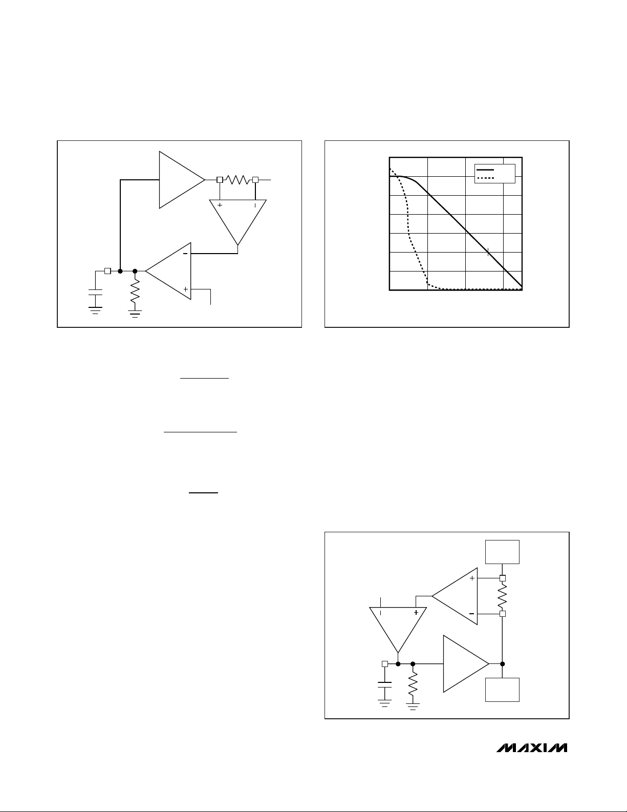
The simplified schematic in Figure 5 is sufficient to
describe the operation of the MAX1909/MAX8725 when
the voltage loop (CCV) is in control. The required compensation network is a pole-zero pair formed with C
CV
and RCV. The pole is necessary to roll off the voltage
loop’s response at low frequency. The zero is necessary
to compensate the pole formed by the output capacitor
and the load. R
ESR
is the equivalent series resistance
(ESR) of the charger output capacitor (C
OUT
). RLis the
equivalent charger output load, where RL= ΔV
BATT
/
ΔI
CHG
. The equivalent output impedance of the GMV
amplifier, R
OGMV
, is greater than 10MΩ. The voltage
loop transconductance (GMV = I
CCV
/ V
BATT
) depends
on the MODE input, which determines the number of
cells. GMV = 0.125mA/mV for 4 cells and GMV =
0.167mA/mV for 3 cells. The DC-DC converter transconductance is dependent upon the charge current-sense
resistor RS2:
where A
CSI
= 20, and RS2 = 0.015Ω in the
Typical
Operating Circuits
(Figures 1 and 2), so GM
OUT
=
3.33A/V.
The loop transfer function is:
LTF GM
RsCR
sC R
R
sC R
GsCR
OUT
OGMV CV CV
CV OGMV
L
OUT L
MV OUT ESR
=×
×+ ×
()
+×
()
×
+×
()
+×
()
1
1
1
1
GM
ARS
OUT
CSI
=
×12
C
CV
C
OUT
R
CV
R
LR
ESR
R
OGMV
CCV
BATT
GMV
REF
GM
OUT
Figure 5. CCV Loop Diagram
NAME CALCULATION DESCRIPTION
1
Lowest frequency pole created by CCV and GMV’s finite output
resistance. Since R
OGMV
is very large and not well controlled, the
exact value for the pole frequency is also not well controlled
(R
OGMV
> 10MΩ).
2
Voltage-loop compensation zero. If this zero is at the same
frequency or lower than the output pole f
P_OUT
, then the loop
transfer function approximates a single pole response near the
crossover frequency. Choose C
CV
to place this zero at least one
decade below crossover to ensure adequate phase margin.
3
Output pole formed with the effective load resistance RL and the
output capacitance C
OUT
. RL influences the DC gain but does not
affect the stability of the system or the crossover frequency.
4
Output ESR Zero. This zero can keep the loop from crossing unity
gain if f
Z_OUT
is less than the desired crossover frequency;
therefore, choose a capacitor with an ESR zero greater than the
crossover frequency.
Table 1. Poles and Zeros of the Voltage-Loop Transfer Function
f
RC
PCV
OGMV CV
_
=
×
1
2π
f
RC
ZCV
CV CV
_
=
×
1
2π
f
RC
P OUT
L OUT
_
=
×
1
2π
f
RC
Z OUT
ESR OUT
_
=
×
1
2π
NO.
CCV pole
CCV zero
Output pole
Output zero
Page 23

MAX1909/MAX8725
Multichemistry Battery Chargers with Automatic
System Power Selector
______________________________________________________________________________________ 23
The poles and zeros of the voltage-loop transfer function
are listed from lowest frequency to highest frequency in
Table 1.
Near crossover, C
CV
has a much lower impedance
than R
OGMV
. Since CCVis in parallel with R
OGMV, CCV
dominates the parallel impedance near crossover.
Additionally, RCVhas a much higher impedance than
CCVand dominates the series combination of RCVand
C
CV
, so:
C
OUT
also has a much lower impedance than RLnear
crossover, so the parallel impedance is mostly capacitive and:
If R
ESR
is small enough, its associated output zero has
a negligible effect near crossover and the loop-transfer
function can be simplified as follows:
Setting the LTF = 1 to solve for the unity-gain frequency
yields:
For stability, choose a crossover frequency lower than
1/10th of the switching frequency. Choosing a
crossover frequency of 30kHz and solving for R
CV
using the component values listed in Figure 1 yields:
MODE = VCC(4 cells)
GMV = 0.125µA/mV
C
OUT
= 22µF
V
BATT
= 16.8V
RL= 0.2Ω
GM
OUT
= 3.33A/V
f
CO_CV
= 30kHz
f
OSC
= 400kHz
To ensure that the compensation zero adequately cancels the output pole, select f
Z_CV
≤ f
P_OUT
:
CCV≥ (RL/RCV) C
OUT
where CCV≥ 4nF (assuming 4 cells and 4A maximum
charge current).
Figure 6 shows the Bode plot of the voltage-loop frequency response using the values calculated above.
CCI Loop Compensation
The simplified schematic in Figure 7 is sufficient to
describe the operation of the MAX1909/MAX8725 when
the battery current loop (CCI) is in control. Since the
output capacitor’s impedance has little effect on the
response of the current loop, only a single pole is
required to compensate this loop. A
CSI
is the internal
gain of the current-sense amplifier. RS2 is the charge
current-sense resistor, RS2 = 15mΩ. R
OGMI
is the
equivalent output impedance of the GMI amplifier,
which is greater than 10MΩ. GMI is the charge-current
amplifier transconductance = 1µA/mV. GM
OUT
is the
DC-DC converter transconductance = 3.3A/V.
The loop transfer function is given by:
LTF GM A RS GMI
R
sR C
OUT CSI
OGMI
OGMI CI
=×××
+×
2
1
R
Cf
GMV GM
k
CV
OUT CO CV
OUT
=
××
×
=210
π
_
Ω
f
CO CV GM GMV
R
C
OUT
CV
OUT
_
=
×
×
⎛
⎝
⎜
⎞
⎠
⎟
2π
LTF GM
R
sC
GMV
OUT
CV
OUT
=×
R
sC R sC
L
OUT L OUT
11+×
()
≅
RsCR
sC R
R
OGMV CV CV
CV OGMV
CV
×+ ×
()
+×
()
≅
1
1
FREQUENCY (Hz)
MAGNITUDE (dB)
PHASE (DEGREES)
100k10k1k100101
-20
0
20
40
60
80
-40
-90
-45
0
-135
0.1 1M
MAG
PHASE
Figure 6. CCV Loop Response
Page 24
MAX1909/MAX8725
Multichemistry Battery Chargers with Automatic
System Power Selector
24 ______________________________________________________________________________________
This describes a single-pole system. Since:
the loop transfer function simplifies to:
The crossover frequency is given by:
For stability, choose a crossover frequency lower than
1/10th of the switching frequency:
C
CI
= GMI / (2π f
O_CI
)
Choosing a crossover frequency of 30kHz and using the
component values listed in Figure 1 yields CCI> 5.4nF.
Values for CCIgreater than 10 times the minimum value
may slow down the current-loop response excessively.
Figure 8 shows the Bode plot of the current-loop frequency response using the values calculated above.
CCS Loop Compensation
The simplified schematic in Figure 9 is sufficient to
describe the operation of the MAX1909/MAX8725 when
the input current-limit loop (CCS) is in control. Since the
output capacitor’s impedance has little effect on the
response of the input current-limit loop, only a single
pole is required to compensate this loop. A
CSS
is the
internal gain of the current-sense amplifier. RS1 is the
input current-sense resistor; RS1 = 10mΩ in the typical
operating circuits. R
OGMS
is the equivalent output
impedance of the GMS amplifier, which is greater than
10MΩ. GMS is the input current amplifier transconductance = 1µA/mV. GMINis the DC-DC converter’s inputreferred transconductance = (1/D) GM
OUT
= (1/D)
3.3A/V.
f
GMI
C
CO CICI_
=
2π
LTF GMI
R
sR C
OGMI
OGMI CI
=
+×1
GM
ARS
OUT
CSI
=
×12
FREQUENCY (Hz)
MAGNITUDE (dB)
100k1k10
-20
0
20
40
60
100
80
-40
-45
0
-90
0.1
MAG
PHASE
Figure 8. CCI Loop Response
C
CS
R
OGMS
GMS
CSS
CLS
CCS
CSSP
RS1
CSSN
GM
IN
SYSTEM
LOAD
ADAPTER
INPUT
Figure 9. CCS Loop Diagram
C
CI
R
OGMI
CCI
GMI
CSI
ICTL
GM
OUT
CSIP
RS2
CSIN
Figure 7. CCI Loop Diagram
Page 25

MAX1909/MAX8725
Multichemistry Battery Chargers with Automatic
System Power Selector
______________________________________________________________________________________ 25
The loop transfer function is given by:
Since:
the loop transfer function simplifies to:
The crossover frequency is given by:
For stability, choose a crossover frequency lower than
1/10th the switching frequency:
CCS= GMS / (2π f
CO_CS
)
Choosing a crossover frequency of 30kHz and using
the component values listed in Figure 1 yields CCS>
5.4nF. Values for CCSgreater than 10 times the minimum value may slow down the input current-loop
response excessively. Figure 10 shows the Bode plot of
the input current-limit loop frequency response using
the values calculated above.
MOSFET Drivers
The DHI and DLO outputs are optimized for driving
moderately-sized power MOSFETs. The MOSFET drive
capability is the same for both the low-side and highside switches. This is consistent with the variable duty
factor that occurs in the notebook computer environment where the battery voltage changes over a wide
range. An adaptive dead-time circuit monitors the DLO
output and prevents the high-side FET from turning on
until DLO is fully off. There must be a low-resistance,
low-inductance path from the DLO driver to the
MOSFET gate for the adaptive dead-time circuit to work
properly. Otherwise, the sense circuitry in the
MAX1909/MAX8725 interpret the MOSFET gate as “off”
while there is still charge left on the gate. Use very
short, wide traces measuring 10 squares to 20 squares
or less (1.25mm to 2.5mm wide if the MOSFET is 25mm
from the device). Unlike the DLO output, the DHI output
uses a fixed-delay 50ns time to prevent the low-side
FET from turning on until DHI is fully off. The same layout considerations should be used for routing the DHI
signal to the high-side FET.
Since the transition time for a p-channel switch can be
much longer than an n-channel switch, the dead time
prior to the high-side PMOS turning on is more pronounced than in other synchronous step-down regulators, which use high-side n-channel switches. On the
high-to-low transition, the voltage on the inductor’s
“switched” terminal flies below ground until the low-side
switch turns on. A similar dead-time spike occurs on
the opposite low-to-high transition. Depending upon the
magnitude of the load current, these spikes usually
have a minor impact on efficiency.
The high-side driver (DHI) swings from SRC to 5V
below SRC and typically sources 0.9A and sinks 0.5A
from the gate of the p-channel FET. The internal pullhigh transistors that drive DHI high are robust, with a
2.0Ω (typ) on-resistance.
The low-side driver (DLO) swings from DLOV to ground
and typically sources 0.5A and sinks 0.9A from the gate
of the n-channel FET. The internal pulldown transistors
that drive DLO low are robust, with a 1.0Ω (typ) onresistance. This helps prevent DLO from being pulled
up when the high-side switch turns on, due to capacitive coupling from the drain to the gate of the low-side
MOSFET. This places some restrictions on the FETs
that can be used. Using a low-side FET with smaller
gate-to-drain capacitance can prevent these problems.
f
GMS
C
CO CSCS_
=
2π
LTF GMS
R
sR C
OGMS
OGMS CS
=
+×1
GM
ARS
IN
CSS
=
×11
LTF GM A RS GMS
R
sR C
IN CSS
OGMS
OGMS CS
=×××
+×
1
1
FREQUENCY (Hz)
MAGNITUDE (dB)
100k 10M1k10
-20
0
20
40
60
100
80
-40
-45
0
-90
0.1
MAG
PHASE
PHASE (DEGREES)
Figure 10. CCS Loop Response
Page 26

MAX1909/MAX8725
Multichemistry Battery Chargers with Automatic
System Power Selector
26 ______________________________________________________________________________________
Design Procedure
Table 2 lists the recommended components and refers
to the circuit of Figure 2. The following sections
describe how to select these components.
MOSFET Selection
MOSFETs P2 and P3 (Figure 1) provide power to the
system load when the AC adapter is inserted. These
devices may have modest switching speeds, but must
be able to deliver the maximum input current as set by
RS1. As always, care should be taken not to exceed
the device’s maximum voltage ratings or the maximum
operating temperature.
The p-channel/n-channel MOSFETs (P1, N1) are the
switching devices for the buck controller. The guidelines
for these devices focus on the challenge of obtaining
high load-current capability when using high-voltage
(>20V) AC adapters. Low-current applications usually
require less attention. The high-side MOSFET (P1) must
be able to dissipate the resistive losses plus the switching
losses at both V
DCIN(MIN)
and V
DCIN(MAX)
.
Ideally, the losses at V
DCIN(MIN)
should be roughly equal
to losses at V
DCIN(MAX)
, with lower losses in between. If
the losses at V
DCIN(MIN)
are significantly higher than the
losses at V
DCIN(MAX)
, consider increasing the size of P1.
Conversely, if the losses at V
DCIN(MAX)
are significantly
higher than the losses at V
DCIN(MIN),
consider reducing
the size of P1. If DCIN does not vary over a wide range,
the minimum power dissipation occurs where the resistive
losses equal the switching losses.
DESCRIPTION
C1, C4
22µF ±20%, 35V E-size low-ESR
tantalum capacitors
AVX TPSE226M035R0300
Kemet T495X226M035AS
C5, C15
1µF ±10%, 25V, X7R ceramic capacitors
(1206)
Murata GRM31MR71E105K
Taiyo Yuden TMK316BJ105KL
TDK C3216X7R1E105K
C9, C10
0.01µF ±10%, 25V, X7R ceramic
capacitors (0402)
Murata GRP155R71E103K
TDK C1005X7R1E103K
C11, C14,
C17
0.1µF ±10%, 25V, X7R ceramic
capacitors (0603)
Murata GRM188R71E104K
TDK C1608X7R1E104K
C12, C13,
C16
1µF ±10%, 6.3V, X5R ceramic
capacitors (0603)
Murata GRM188R60J105K
Taiyo Yuden JMK107BJ105KA
TDK C1608X5R1A105K
D4
Schottky diode, 0.5A, 30V SOD-123
Diodes Inc. B0530W
General Semiconductor MBR0530
ON Semiconductor MBR0530
D5
25V ±1% zener diode
CMDZ5253B
L1
10µH, 4.4A inductor
Sumida CDRH104R-100NC
TOKO 919AS-100M
Table 2. Recommended Components
REFERENCE
QTY
DESCRIPTION
N1/P1
Dual n- and p-channel MOSFETs, 7A,
30V and -5A, -30V, 8-pin SO, MOSFET
Fairchild FDS8958A or
Single n-channel MOSFETs, +13.5A,
+30V FDS6670S and
Single p-channel MOSFETs, -13.5A,
-30V FDS66709Z
Single, p-channel, -11A, -30V, 8-pin SO
MOSFETs
Fairchild FDS6675
R4
100kΩ, ±5% resistor (0603)
10kΩ ±1% resistors (0603)
R6
590kΩ ±1% resistor (0603)
R7
196kΩ ±1% resistor (0603)
R8
1MΩ ±5% resistor (0603)
R11
1kΩ ±5% resistor (0603)
R16
33Ω ±5% resistor (0603)
R19, R20
10kΩ ±5% resistors (0603)
RS1
0.01Ω ±1%, 0.5W sense resistor (2010)
Vishay Dale WSL2010 0.010 1.0%
IRC LRC-LR2010-01-R010-F
RS2
0.015Ω ±1%, 0.5W sense resistor (2010)
Vishay Dale WSL2010 0.015 1.0%
IRC LRC-LR2010-01-R015-F
U1
MAX1909ETI/MAX8725ETI (28-pin thin
QFN-EP)
REFERENCE QTY
2
1
2
P2, P3, P4 3
2
3
3
1
1
1
1
R5, R9, R21 2
1
1
1
1
1
2
1
1
1
Page 27

MAX1909/MAX8725
Multichemistry Battery Chargers with Automatic
System Power Selector
______________________________________________________________________________________ 27
Choose a low-side MOSFET that has the lowest possible on-resistance (R
DS(ON)
), comes in a moderatesized package, and is reasonably priced. Make sure
that the DLO gate driver can supply sufficient current to
support the gate charge and the current injected into
the parasitic gate-to-drain capacitor caused by the
high-side MOSFET turning on; otherwise, cross-conduction problems can occur.
The MAX1909/MAX8725 have an adaptive dead-time circuit that prevents the high-side and low-side MOSFETs
from conducting at the same time (see the
MOSFET
Drivers
section). Even with this protection, it is still possible for delays internal to the MOSFET to prevent one
MOSFET from turning off when the other is turned on.
Select devices that have low turn-off times. To be
conservative, make sure that P1(t
DOFF(MAX)
) -
N1(t
DON(MIN)
) < 40ns. Failure to do so may result in
efficiency-killing shoot-through currents. If delay mismatch causes shoot-through currents, consider adding
extra capacitance from gate to source on N1 to slow
down its turn-on time.
MOSFET Power Dissipation
Worst-case conduction losses occur at the duty factor
extremes. For the high-side MOSFET, the worst-case
power dissipation (PD) due to resistance occurs at the
minimum supply voltage:
Generally, a small high-side MOSFET is desired to
reduce switching losses at high input voltages.
However, the R
DS(ON)
required to stay within package
power-dissipation limits often limits how small the
MOSFET can be. The optimum occurs when the switching (AC) losses equal the conduction (I2R
DS(ON)
)
losses. High-side switching losses do not usually
become an issue until the input is greater than approximately 15V. Switching losses in the high-side MOSFET
can become an insidious heat problem when maximum
AC adapter voltages are applied, due to the squared
term in the CV2f switching-loss equation. If the highside MOSFET that was chosen for adequate R
DS(ON)
at
low supply voltages becomes extraordinarily hot when
subjected to V
DCIN(MAX),
then choose a MOSFET with
lower losses. Calculating the power dissipation in P1
due to switching losses is difficult since it must allow for
difficult quantifying factors that influence the turn-on
and turn-off times. These factors include the internal
gate resistance, gate charge, threshold voltage, source
inductance, and PC board layout characteristics. The
following switching-loss calculation provides only a very
rough estimate and is no substitute for breadboard
evaluation, preferably including a verification using a
thermocouple mounted on P1:
where C
RSS
is the reverse transfer capacitance of P1,
and I
GATE
is the peak gate-drive source/sink current.
For the low-side MOSFET (N1), the worst-case power
dissipation always occurs at maximum input voltage:
Choose a Schottky diode (D1, Figure 2) with a forward
voltage low enough to prevent the N1 MOSFET body
diode from turning on during the dead time. As a general rule, a diode with a DC current rating equal to 1/3rd
the load current is sufficient. This diode is optional and
can be removed if efficiency is not critical.
Inductor Selection
The charge current, ripple, and operating frequency
(off-time) determine the inductor characteristics.
Inductor L1 must have a saturation current rating of at
least the maximum charge current plus 1/2 of the ripple
current (ΔIL):
I
SAT
= I
CHG
+ (1/2) ΔIL
PD N
V
V
I
R
BATT
DCIN
LOAD
DS ON
()
()
11
2
2
=
⎛
⎝
⎜
⎞
⎠
⎟
⎡
⎣
⎢
⎢
⎤
⎦
⎥
⎥
⎛
⎝
⎜
⎞
⎠
⎟
×
−
PD P Switching
VCfI
I
DCIN MAX RSS SW LOAD
GATE
(_ )
()
1
2
2
=
×××
PD P
V
V
I
R
BATT
DCIN
LOAD
DS ON
()
()
1
2
2
=
⎛
⎝
⎜
⎞
⎠
⎟
⎛
⎝
⎜
⎞
⎠
⎟
×
0
1.0
0.5
1.5
8 101112139 1415161718
V
BATT
(V)
RIPPLE CURRENT (A)
V
DCIN
= 19V
VCTL = ICTL = LDO
3 CELLS
4 CELLS
Figure 11. Ripple Current vs. Battery Voltage (MAX1909)
Page 28

MAX1909/MAX8725
Multichemistry Battery Chargers with Automatic
System Power Selector
28 ______________________________________________________________________________________
The ripple current is determined by:
ΔIL = V
BATTtOFF
/ L
where:
t
OFF
= 2.5µs (V
DCIN
- V
BATT
) / V
DCIN
for
V
BATT
< 0.88 V
DCIN
or:
t
OFF
= 0.3µs for V
BATT
> 0.88 V
DCIN
Figure 11 illustrates the variation of the ripple current
vs. battery voltage when the circuit is charging at 3A
with a fixed input voltage of 19V.
Higher inductor values decrease the ripple current.
Smaller inductor values require high-saturation current
capabilities and degrade efficiency. Designs that set
LIR = ΔIL / I
CHG
= 0.3 usually result in a good balance
between inductor size and efficiency.
Input-Capacitor Selection
The input capacitor must meet the ripple current
requirement (I
RMS
) imposed by the switching currents.
Nontantalum chemistries (ceramic, aluminum, or OSCON) are preferred due to their resilience to power-up
surge currents.
The input capacitors should be sized so that the
temperature rise due to ripple current in continuous
conduction does not exceed approximately 10°C. The
maximum ripple current occurs at 50% duty factor or
V
DCIN
= 2 V
BATT
, which equates to 0.5 I
CHG
. If the
application of interest does not achieve the maximum
value, size the input capacitors according to the
worst-case conditions.
Output-Capacitor Selection
The output capacitor absorbs the inductor ripple current and must tolerate the surge current delivered from
the battery when it is initially plugged into the charger.
As such, both capacitance and ESR are important
parameters in specifying the output capacitor as a filter
and to ensure the stability of the DC-DC converter (see
the
Compensation
section). Beyond the stability
requirements, it is often sufficient to make sure that the
output capacitor’s ESR is much lower than the battery’s
ESR. Either tantalum or ceramic capacitors can be
used on the output. Ceramic devices are preferable
because of their good voltage ratings and resilience to
surge currents.
Applications Information
Startup Conditioning Charge for
Overdischarged Cells
It is desirable to charge deeply discharged Li+ batteries at a low rate to improve cycle life. The
MAX1909/MAX8725 automatically reduces the charge
current when the voltage per cell is below 3.1V. The
charge current-sense voltage is set to 4.5mV (I
CHG
=
300mA with RS2 = 15mΩ) until the battery voltage rises
above the threshold. There is approximately 300mV for
3 cell, 400mV for 4 cell of hysteresis to prevent the
charge-current magnitude from chattering between the
two values.
For the MAX8725, control the ICTL voltage to set a conditioning charge rate.
Layout and Bypassing
Bypass DCIN with a 1µF capacitor to ground (Figure 1).
D4 protects the MAX1909/MAX8725 when the DC
power source input is reversed. A signal diode for D4 is
adequate because DCIN only powers the LDO and the
internal reference. Bypass LDO, DHIV, DLOV, and
other pins as shown in Figure 1.
Good PC board layout is required to achieve specified
noise, efficiency, and stable performance. The PC
board layout artist must be given explicit instructions—
preferably, a sketch showing the placement of the
power-switching components and high-current routing.
Refer to the PC board layout in the MAX1909/MAX8725
evaluation kit for examples. A ground plane is essential
for optimum performance. In most applications, the circuit is located on a multilayer board, and full use of the
four or more copper layers is recommended. Use the
top layer for high-current connections, the bottom layer
for quiet connections, and the inner layers for an uninterrupted ground plane.
Use the following step-by-step guide:
1) Place the high-power connections first, with their
grounds adjacent:
a) Minimize the current-sense resistor trace
lengths, and ensure accurate current sensing
with Kelvin connections.
b) Minimize ground trace lengths in the high-current
paths.
c) Minimize other trace lengths in the high-current
paths.
d) Use >5mm wide traces.
II
VV V
V
RMS CHG
BATT DCIN BATT
DCIN
=
⎛
⎝
⎜
⎜
⎞
⎠
⎟
⎟
−()
Page 29

MAX1909/MAX8725
Multichemistry Battery Chargers with Automatic
System Power Selector
______________________________________________________________________________________ 29
e) Connect C1 and C2 to the high-side MOSFET
(10mm max length). Return these capacitors to
the power ground plane.
f) Minimize the LX node (MOSFETs, rectifier cath-
ode, inductor (15mm max length)).
Ideally, surface-mount power components are
flush against one another with their ground
terminals almost touching. These high-current
grounds are then connected to each other with
a wide, filled zone of top-layer copper, so they
do not go through vias.
The resulting top-layer ground plane is connected
to the normal inner-layer ground plane at the output ground terminals, which ensures that the IC’s
analog ground is sensing at the supply’s output
terminals without interference from IR drops and
ground noise. Other high-current paths should
also be minimized, but focusing primarily on short
ground and current-sense connections eliminates
about 90% of all PC board layout problems.
2) Place the IC and signal components. Keep the main
switching node (LX node) away from sensitive analog components (current-sense traces and REF
capacitor). Important: the IC should be less than
10mm from the current-sense resistors.
Quiet connections to REF, VCTL, ICTL, CCV, CCI,
CCS, IINP, ACIN, and DCIN should be returned to a
separate ground (GND) island. The appropriate
traces are marked on the schematic with the
ground symbol ( ). There is very little current flowing in these traces, so the ground island need not
be very large. When placed on an inner layer, a sizable ground island can help simplify the layout
because the low-current connections can be made
through vias. The ground pad on the backside of
the package should also be connected to this quiet
ground island.
3) Keep the gate drive traces (DHI and DLO) as short
as possible (L < 20mm), and route them away from
the current-sense lines and REF. These traces
should also be relatively wide (W > 1.25mm).
4) Place ceramic bypass capacitors close to the IC.
The bulk capacitors can be placed further away.
5) Use a single-point star ground placed directly
below the part at the PGND pin. Connect the power
ground (ground plane) and the quiet ground island
at this location. See Figure 12.
Chip Information
TRANSISTOR COUNT: 2720
PROCESS: BiCMOS
INDUCTOR
C
IN
C
OUT
C
OUT
INPUT
OUTPUT
KELVIN-SENSE VIAS
UNDER THE SENSE
RESISTOR
(REFER TO EVALUATION KIT)
GND
PGND
POWER PATH
QUIET GROUND
ISLAND
Figure 12. PC Board Layout Examples
Page 30

MAX1909/MAX8725
Multichemistry Battery Chargers with Automatic
System Power Selector
Maxim cannot assume responsibility for use of any circuitry other than circuitry entirely embodied in a Maxim product. No circuit patent licenses are
implied. Maxim reserves the right to change the circuitry and specifications without notice at any time.
30
____________________Maxim Integrated Products, 120 San Gabriel Drive, Sunnyvale, CA 94086 408-737-7600
© 2004 Maxim Integrated Products Printed USA is a registered trademark of Maxim Integrated Products.
Package Information
(The package drawing(s) in this data sheet may not reflect the most current specifications. For the latest package outline information,
go to www.maxim-ic.com/packages
.)
Package Information
(The package drawing(s) in this data sheet may not reflect the most current specifications. For the latest package outline information,
go to www.maxim-ic.com/packages
.)
Package Information
(The package drawing(s) in this data sheet may not reflect the most current specifications. For the latest package outline information,
go to www.maxim-ic.com/packages
.)
QFN THIN.EPS
 Loading...