

Page 1
General Description
The MAX1908/MAX8724/MAX8765 highly integrated, multichemistry battery-charger control ICs simplify the construction of accurate and efficient chargers. These devices use
analog inputs to control charge current and voltage, and
can be programmed by the host or hardwired. The
MAX1908/MAX8724/MAX8765 achieve high efficiency
using a buck topology with synchronous rectification.
The MAX1908/MAX8724/MAX8765 feature input current
limiting. This feature reduces battery charge current when
the input current limit is reached to avoid overloading the
AC adapter when supplying the load and the battery
charger simultaneously. The MAX1908/MAX8724/
MAX8765 provide outputs to monitor current drawn from
the AC adapter (DC input source), battery-charging current, and the presence of an AC adapter. The MAX1908’s
conditioning charge feature provides 300mA to safely
charge deeply discharged lithium-ion (Li+) battery packs.
The MAX1908 includes a conditioning charge feature
while the MAX8724/MAX8765 do not.
The MAX1908/MAX8724/MAX8765 charge two to four
series Li+ cells, providing more than 5A, and are available in a space-saving, 28-pin, thin QFN package (5mm
× 5mm). An evaluation kit is available to speed designs.
Applications
Notebook and Subnotebook Computers
Personal Digital Assistants
Handheld Terminals
Features
♦ ±0.5% Output Voltage Accuracy Using Internal
Reference (0°C to +85°C)
♦ ±4% Accurate Input Current Limiting
♦ ±5% Accurate Charge Current
♦ Analog Inputs Control Charge Current and
Charge Voltage
♦ Outputs for Monitoring
Current Drawn from AC Adapter
Charging Current
AC Adapter Presence
♦ Up to 17.6V Battery-Voltage Set Point
♦ Maximum 28V Input Voltage
♦ > 95% Efficiency
♦ Shutdown Control Input
♦ Charge Any Battery Chemistry
Li+, NiCd, NiMH, Lead Acid, etc.
MAX1908/MAX8724/MAX8765
Low-Cost Multichemistry Battery Chargers
________________________________________________________________ Maxim Integrated Products 1
28
27
26
25
24
23
22
IINP
CSSP
CSSN
DHI
BST
LX
DLOV
8
9
10
11
12
13
14
SHDN
ICHG
ACIN
ACOK
REFIN
ICTL
GND
15161718192021
VCTL
BATT
CELLS
CSIN
CSIP
PGND
DLO
7654321
CCV
CCI
CCS
REF
CLS
LDO
DCIN
MAX1908
MAX8724
MAX8765
THIN QFN
TOP VIEW
Pin Configuration
Ordering Information
MAX1908
MAX8724
MAX8765
AC ADAPTER
INPUT
TO EXTERNAL
LOAD
LDO
FROM HOST μP
10μH
0.015Ω
BATT+
DCIN
REFIN
VCTL
ICTL
ACIN
ACOK
SHDN
ICHG
IINP
CCV
CCI
CCS
CELLS
LDO
BST
DLOV
DHI
LX
DLO
PGND
CSIP
CSIN
BATT
REF CLS
GND
CSSP CSSN
0.01Ω
Minimum Operating Circuit
19-2764; Rev 4; 7/05
For pricing, delivery, and ordering information, please contact Maxim/Dallas Direct! at
1-888-629-4642, or visit Maxim’s website at www.maxim-ic.com.
EVALUATION KIT
AVAILABLE
PART
TEMP RANGE
PIN-
PKG CODE
MAX1908ETI
T2855-6
MAX8724ETI
T2855-6
MAX8765ETI
T2855-6
PACKAGE
-40°C to +85°C 28 Thin QFN
-40°C to +85°C 28 Thin QFN
-40°C to +85°C 28 Thin QFN
Page 2
MAX1908/MAX8724/MAX8765
Low-Cost Multichemistry Battery Chargers
2 _______________________________________________________________________________________
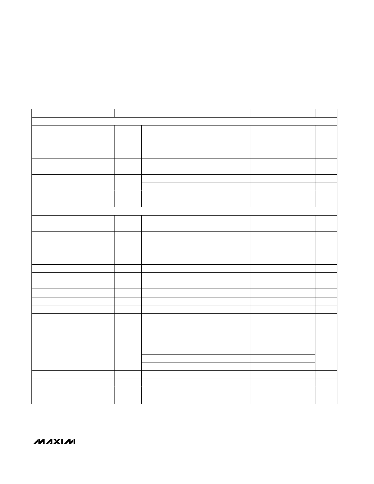
ABSOLUTE MAXIMUM RATINGS
ELECTRICAL CHARACTERISTICS
(V
DCIN
= V
CSSP
= V
CSSN
= 18V, V
BATT
= V
CSIP
= V
CSIN
= 12V, V
REFIN
= 3V, V
VCTL
= V
ICTL
= 0.75 x V
REFIN
, CELLS = float, CLS =
REF, V
BST
- VLX= 4.5V, ACIN = GND = PGND = 0, C
LDO
= 1µF, LDO = DLOV, C
REF
= 1µF; CCI, CCS, and CCV are compensated
per Figure 1a; T
A
= 0°C to +85°C, unless otherwise noted. Typical values are at TA= +25°C.)
Stresses beyond those listed under “Absolute Maximum Ratings” may cause permanent damage to the device. These are stress ratings only, and functional
operation of the device at these or any other conditions beyond those indicated in the operational sections of the specifications is not implied. Exposure to
absolute maximum rating conditions for extended periods may affect device reliability.
DCIN, CSSP, CSSN, ACOK to GND.......................-0.3V to +30V
BST to GND ............................................................-0.3V to +36V
BST to LX..................................................................-0.3V to +6V
DHI to LX...................................................-0.3V to (V
BST
+ 0.3V)
LX to GND .................................................................-6V to +30V
BATT, CSIP, CSIN to GND .....................................-0.3V to +20V
CSIP to CSIN or CSSP to CSSN or
PGND to GND ....................................................-0.3V to +0.3V
CCI, CCS, CCV, DLO, ICHG,
IINP, ACIN, REF to GND.......................-0.3V to (V
LDO
+ 0.3V)
DLOV, VCTL, ICTL, REFIN, CELLS, CLS,
LDO, SHDN to GND .............................................-0.3V to +6V
DLOV to LDO.........................................................-0.3V to +0.3V
DLO to PGND .........................................-0.3V to (V
DLOV
+ 0.3V)
LDO Short-Circuit Current...................................................50mA
Continuous Power Dissipation (T
A
= +70°C)
28-Pin Thin QFN (5mm × 5mm)
(derate 20.8mW/°C above +70°C) .........................1666.7mW
Operating Temperature Range ..........................-40°C to +85°C
Junction Temperature......................................................+150°C
Storage Temperature Range .............................-60°C to +150°C
Lead Temperature (soldering, 10s) .................................+300°C
PARAMETER
CONDITIONS
UNITS
CHARGE-VOLTAGE REGULATION
V
VCTL
= V
REFIN
(2, 3, or 4 cells)
V
VCTL
= V
REFIN
/ 20 (2, 3, or 4 cells)
Battery-Regulation Voltage
Accuracy
V
VCTL
= V
LDO
(2, 3, or 4 cells)
%
VCTL Default Threshold V
VCTL
rising 4.0 4.1 4.2 V
REFIN Range (Note 1) 2.5 3.6 V
REFIN Undervoltage Lockout V
REFIN
falling
V
CHARGE-CURRENT REGULATION
CSIP-to-CSIN Full-Scale Current-
Sense Voltage
V
ICTL
= V
REFIN
75
mV
V
ICTL
= V
REFIN
-5 +5
V
ICTL
= V
REFIN
x 0.6 -5 +5
V
ICTL
= V
LDO
-6 +6
MAX8765 only; V
ICTL
= V
REFIN
x 0.036 -45
Charging-Current Accuracy
MAX8724 only; V
ICTL
= V
REFIN
x 0.058 -33
%
Charge-Current Gain Error
(MAX8765 Only)
-2 +2 %
Charge-Current Offset
(MAX8765 Only)
-2 +2 mV
ICTL Default Threshold V
ICTL
rising 4.0 4.1 4.2 V
BATT/CSIP/CSIN Input Voltage
Range
0 19 V
V
DCIN
= 0 or V
ICTL
= 0 or SHDN = 0 1
CSIP/CSIN Input Current
Charging
650
µA
SYMBOL
MIN TYP MAX
-0.5
-0.5
-0.5
71.25
1.20 1.92
400
+0.5
+0.5
+0.5
78.75
+45
+33
Page 3
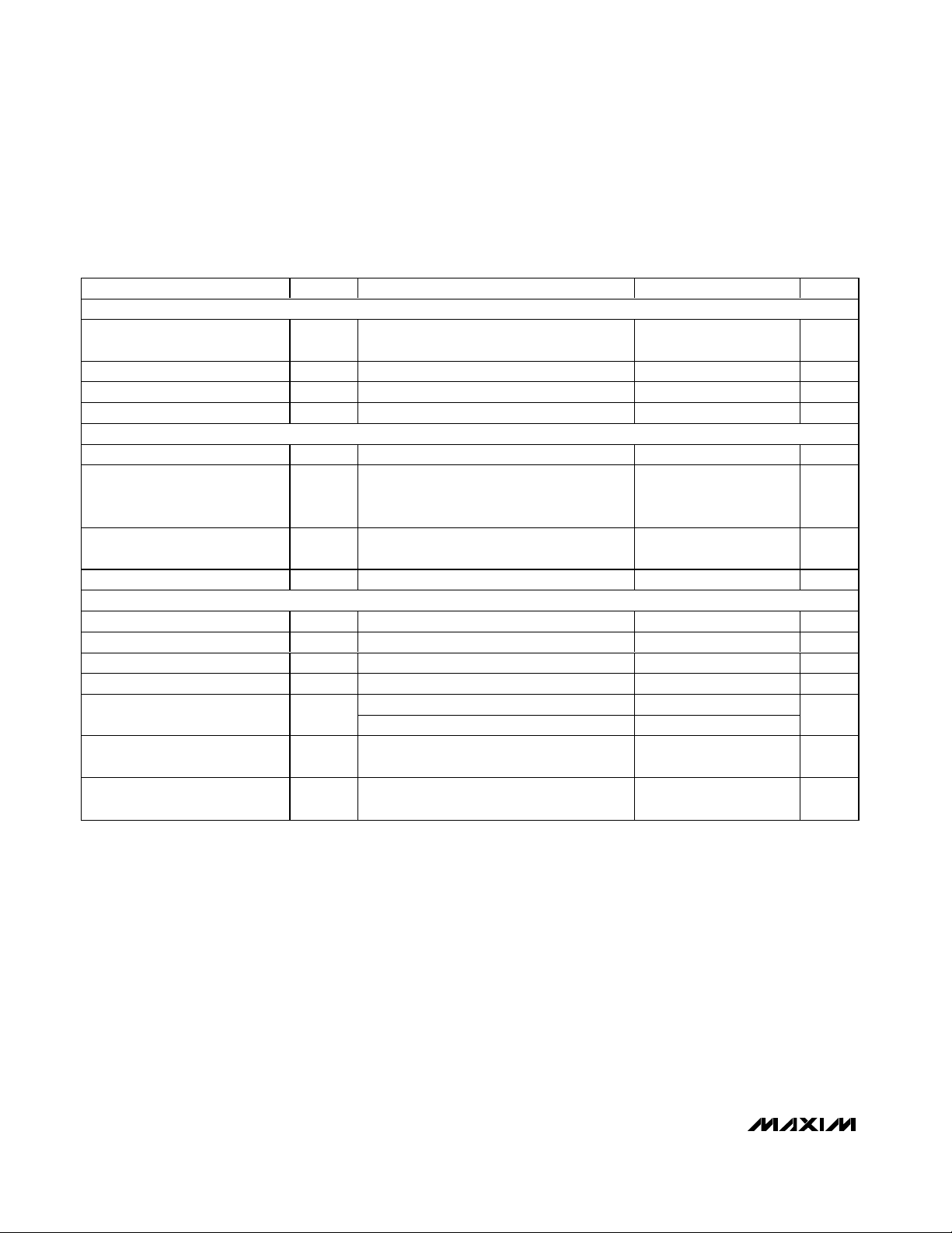
Low-Cost Multichemistry Battery Chargers
ELECTRICAL CHARACTERISTICS (continued)
(V
= V
DCIN
REF, V
BST
per Figure 1a; T
Cycle-by-Cycle Maximum Current
Limit
= V
CSSP
- VLX= 4.5V, ACIN = GND = PGND = 0, C
A
PARAMETER SYMBOL CONDITIONS MIN TYP MAX UNITS
= 18V, V
CSSN
= 0°C to +85°C, unless otherwise noted. Typical values are at TA= +25°C.)
BATT
= V
I
MAX
CSIP
= V
= 12V, V
CSIN
LDO
REFIN
= 1µF, LDO = DLOV, C
RS2 = 0.015Ω 6.0 6.8 7.5
ICTL Power-Down Mode
Threshold Voltage
(MAX1908/MAX8724 Only)
ICTL, VCTL Input Bias Current
REFIN Input Bias Current
ICHG Transconductance
(MAX1908/MAX8724 Only)
ICHG Transconductance
(MAX8765 Only)
ICHG Transconductance Error
(MAX8765 Only)
ICHG Transconductance Offset
(MAX8765 Only)
ICHG Accuracy
ICHG Output Current V
ICHG Output Voltage V
V
G
ICHG VCSIP
G
ICHG VCSIP
rising
ICTL
V
VCTL
V
DCIN
V
DCIN
V
REFIN
= V
= 0, V
= 5V, V
- V
- V
= 0 or 3V -1 +1
ICTL
= V
VCTL
REFIN
= 5V -1 +1
= 45mV 2.7 3 3.3 µA/mV
CSIN
= 45mV 2.85 3 3.15 µA/mV
CSIN
-5 +5 %
-5 +5 µA
V
- V
= 75mV -6 +6
CSIN
- V
= 45mV -5 +5
CSIN
- V
= 5mV -40 +40
CSIN
- V
= 150mV, V
CSIN
- V
= 150mV, ICHG = float 3.5 V
CSIN
V
V
CSIP
CSIP
CSIP
CSIP
CSIP
INPUT-CURRENT REGULATION
CSSP-to-CSSN Full-Scale
Current-Sense Voltage
Input Current-Limit Gain Error
(MAX8765 Only)
Input Current-Limit Offset
(MAX8765 Only)
CSSP, CSSN Input Voltage
Range
CSSP, CSSN Input Current
(MAX1908/MAX8724 Only)
CSSP Input Current
(MAX8765 Only)
72 75 78 mV
V
= V
CLS
REF
V
= V
/ 2 -7.5 +7.5 Input Current-Limit Accuracy
REF
= 1.1V (MAX8765 only) -10 +10
V
CLS
CLS
-2 +2 %
-2 +2 mV
8 28 V
V
= 0 0.1 1
V
DCIN
V
CSSP
CSSP
= V
= V
CSSN
CSSN
= V
= 28V
= 3V, V
= V
ICTL
= 3V -1 +1
ICHG
= V
VCTL
REF
= 5V -1 +1
REFIN
= 0 350 µA
= 0.75 x V
ICTL
= 1µF; CCI, CCS, and CCV are compensated
REFIN /
100
, CELLS = float, CLS =
REFIN
REFIN /55 REFIN
/ 33
-4 +4
> 8V 350 600
DCIN
V
= 0V 0.1 1
DCIN
= 28V
V
DCIN
400 650
MAX1908/MAX8724/MAX8765
A
V
µA
µA
%
%
µA
µA
_______________________________________________________________________________________ 3
Page 4
MAX1908/MAX8724/MAX8765
Low-Cost Multichemistry Battery Chargers
4 _______________________________________________________________________________________
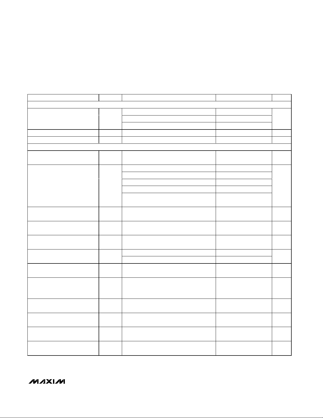
ELECTRICAL CHARACTERISTICS (continued)
(V
DCIN
= V
CSSP
= V
CSSN
= 18V, V
BATT
= V
CSIP
= V
CSIN
= 12V, V
REFIN
= 3V, V
VCTL
= V
ICTL
= 0.75 x V
REFIN
, CELLS = float, CLS =
REF, V
BST
- VLX= 4.5V, ACIN = GND = PGND = 0, C
LDO
= 1µF, LDO = DLOV, C
REF
= 1µF; CCI, CCS, and CCV are compensated
per Figure 1a; T
A
= 0°C to +85°C, unless otherwise noted. Typical values are at TA= +25°C.)
PARAMETER
SYMBOL
CONDITIONS
MIN
TYP
MAX
UNITS
V
DCIN
= 0 0.1 1
CSSN Input Current
(MAX8765 Only)
V
CSSP
= V
CSSN
= 28V
V
DCIN
= 28V 0.1 1
µA
CLS Input Range
(MAX1908/MAX8724 Only)
1.6
V
CLS Input Range
(MAX8765 Only)
1.1
V
CLS Input Bias Current V
CLS
= 2V -1 +1 µA
IINP Transconductance
(MAX1908/MAX8724 Only)
G
IINP
V
CSSP
- V
CSSN
= 75mV 2.7 3 3.3
µA/mV
V
CSSP
- V
CSSN
= 75mV -5 +5
IINP Accuracy
V
CSSP
- V
CSSN
= 37.5mV
%
IINP Transconductance
(MAX8765 Only)
G
IINP
V
CSSP
- V
CCSN
= 75mV
3
µA/mV
IINP Transconductance Error
(MAX8765 Only)
-6 +6 %
IINP Transconductance Offset
(MAX8765 Only)
-10
µA
IINP Output Current V
CSSP
- V
CSSN
= 150mV, V
IINP
= 0
µA
IINP Output Voltage V
CSSP
- V
CSSN
= 150mV, V
IINP
= float 3.5 V
SUPPLY AND LDO REGULATOR
DCIN Input Voltage Range V
DCIN
8 28 V
V
DCIN
falling 7 7.4
DCIN Undervoltage-Lockout Trip
Point
V
DCIN
rising 7.5
V
DCIN Quiescent Current I
DCIN
8.0V < V
DCIN
< 28V 3.2 6 mA
V
BATT
= 19V, V
DCIN
= 0 1
BATT Input Current I
BATT
V
BATT
= 2V to 19V, V
DCIN
= 19.3V
500
µA
LDO Output Voltage 8V < V
DCIN
< 28V, no load
5.4
V
LDO Load Regulation 0 < I
LDO
< 10mA
34 100 mV
LDO Undervoltage-Lockout Trip
Point
V
DCIN
= 8V
4
V
REFERENCE
REF Output Voltage 0 < I
REF
< 500µA
V
REF Undervoltage-Lockout Trip
Point
V
REF
falling 3.1 3.9 V
REF
REF
-7.5
2.82
350
5.25
3.20
4.072 4.096 4.120
200
+7.5
3.18
+10
7.85
5.55
5.15
Page 5
MAX1908/MAX8724/MAX8765
Low-Cost Multichemistry Battery Chargers
_______________________________________________________________________________________ 5
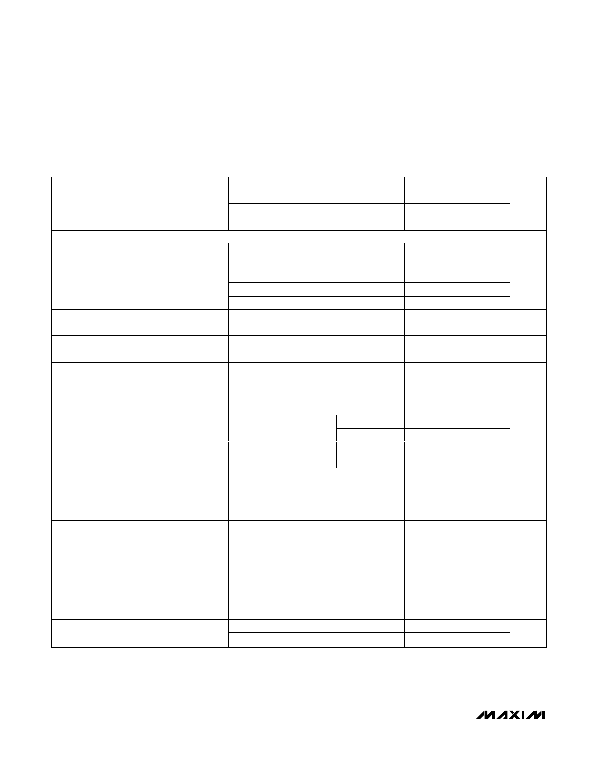
ELECTRICAL CHARACTERISTICS (continued)
(V
DCIN
= V
CSSP
= V
CSSN
= 18V, V
BATT
= V
CSIP
= V
CSIN
= 12V, V
REFIN
= 3V, V
VCTL
= V
ICTL
= 0.75 x V
REFIN
, CELLS = float, CLS =
REF, V
BST
- VLX= 4.5V, ACIN = GND = PGND = 0, C
LDO
= 1µF, LDO = DLOV, C
REF
= 1µF; CCI, CCS, and CCV are compensated
per Figure 1a; T
A
= 0°C to +85°C, unless otherwise noted. Typical values are at TA= +25°C.)
PARAMETER
SYMBOL
CONDITIONS
MIN
TYP
MAX
UNITS
TRIP POINTS
V
DCIN
falling, referred to V
CSIN
(MAX1908/MAX8724 only)
50
150
BATT Power-Fail Threshold
V
CSSP
falling, referred to V
CSIN
(MAX8765 only)
50
150
mV
BATT Power-Fail Threshold
Hysteresis
mV
ACIN rising (MAX8765 only)
V
ACIN Threshold
ACIN rising (MAX1908/MAX8724 only)
V
ACIN Threshold Hysteresis 0.5% of REF 20 mV
ACIN Input Bias Current V
ACIN
= 2.048V -1 +1 µA
SWITCHING REGULATOR
DHI Off-Time
V
BATT
= 16V, V
DCIN
= 19V,
V
CELLS
= V
REFIN
0.4
µs
DHI Minimum Off-Time
V
BATT
= 16V, V
DCIN
= 17V,
V
CELLS
= V
REFIN
µs
DHI Maximum On-Time 2.5 5 7.5 ms
DLOV Supply Current I
DLOV
DLO low 5 10 µA
BST Supply Current I
BST
DHI high 6 15 µA
BST Input Quiescent Current
V
DCIN
= 0, V
BST
= 24.5V,
V
BATT
= VLX = 20V
0.3 1 µA
LX Input Bias Current V
DCIN
= 28V, V
BATT
= VLX = 20V
500 µA
LX Input Quiescent Current V
DCIN
= 0, V
BATT
= VLX = 20V 0.3 1 µA
DHI Maximum Duty Cycle 99
%
Minimum Discontinuous-Mode
Ripple Current
0.5 A
Battery Undervoltage Charge
Current
V
BATT
= 3V per cell (RS2 = 15mΩ),
MAX1908 only, V
BATT
rising
450 mA
CELLS = GND, MAX1908 only, V
BATT
rising 6.1 6.2 6.3
CELLS = float, MAX1908 only, V
BATT
rising
9.3
Battery Undervoltage Current
Threshold
V
DHI On-Resistance High V
BST
- VLX = 4.5V, I
DHI
= +100mA 4 7 Ω
DHI On-Resistance Low V
BST
- V
LX
= 4.5V, I
DHI
= -100mA 1 3.5 Ω
DLO On-Resistance High V
DLOV
= 4.5V, I
DLO
= +100mA
4 7 Ω
DLO On-Resistance Low V
DLOV
= 4.5V, I
DLO
= -100mA
1 3.5 Ω
100
100
200
2.028 2.048 2.068
2.007 2.048 2.089
0.36
0.24 0.28 0.33
150
99.9
CELLS = V
, MAX1908 only, V
REFIN
BATT
rising 12.2 12.4 12.6
150 300
9.15
0.44
9.45
Page 6
MAX1908/MAX8724/MAX8765
Low-Cost Multichemistry Battery Chargers
6 _______________________________________________________________________________________
ELECTRICAL CHARACTERISTICS (continued)
(V
DCIN
= V
CSSP
= V
CSSN
= 18V, V
BATT
= V
CSIP
= V
CSIN
= 12V, V
REFIN
= 3V, V
VCTL
= V
ICTL
= 0.75 x V
REFIN
, CELLS = float, CLS =
REF, V
BST
- VLX= 4.5V, ACIN = GND = PGND = 0, C
LDO
= 1µF, LDO = DLOV, C
REF
= 1µF; CCI, CCS, and CCV are compensated
per Figure 1a; T
A
= 0°C to +85°C, unless otherwise noted. Typical values are at TA= +25°C.)
PARAMETER
SYMBOL
CONDITIONS
MIN
TYP
MAX
UNITS
ERROR AMPLIFIERS
GMV Amplifier Transconductance
GMV
V
V C T L
= V
LD O
, V
BAT T
= 16.8V ,
C E LLS = V
RE F IN
µA/mV
GMI Amplifier Transconductance
GMI V
ICTL
= V
RE F IN
, V
CSIP
- V
CSIN
= 75mV 0.5 1 2.0
µA/mV
GMS Amplifier Transconductance
GMS V
CLS
= V
REF
, V
CSSP
- V
CSSN
= 75mV 0.5 1 2.0
µA/mV
CCI, CCS, CCV Clamp Voltage 0.25V < V
CCV,CCS,CCI
< 2V
600 mV
LOGIC LEVELS
CELLS Input Low Voltage 0.4 V
CELLS Input Float Voltage CELLS = float
(V
REFIN
/ 2) -
0.2V
V
REFIN
/ 2
( V
R E F IN
/ 2) +
V
CELLS Input High Voltage
V
REFIN
V
CELLS Input Bias Current CELLS = 0 or V
REFIN
-2 +2 µA
ACOK AND SHDN
ACOK Input Voltage Range 0 28 V
ACOK Sink Current V
ACOK
= 0.4V, V
ACIN
= 3V 1 mA
ACOK Leakage Current V
ACOK
= 28V, V
ACIN
= 0 1 µA
SHDN Input Voltage Range 0
V
V
SHDN
= 0 or V
LDO
-1 +1
SHDN Input Bias Current
V
DCIN
= 0, V
SHDN
= 5V -1 +1
µA
SHDN Threshold V
SHDN
falling 22
25
% of
V
REFIN
SHDN Threshold Hysteresis 1
% of
V
REFIN
0.0625 0.125 0.2500
150 300
- 0.4V
0.2V
23.5
LDO
Page 7
MAX1908/MAX8724/MAX8765
Low-Cost Multichemistry Battery Chargers
_______________________________________________________________________________________ 7
ELECTRICAL CHARACTERISTICS
(V
DCIN
= V
CSSP
= V
CSSN
= 18V, V
BATT
= V
CSIP
= V
CSIN
= 12V, V
REFIN
= 3V, V
VCTL
= V
ICTL
= 0.75 x V
REFIN
, CELLS = FLOAT, CLS =
REF, V
BST
- VLX= 4.5V, ACIN = GND = PGND = 0, C
LDO
= 1µF, LDO = DLOV, C
REF
= 1µF; CCI, CCS, and CCV are compensated
per Figure 1a; T
A
= -40°C to +85°C, unless otherwise noted.) (Note 2)
PARAMETER
SYMBOL
CONDITIONS
MIN
TYP
MAX
UNITS
CHARGE-VOLTAGE REGULATION
V
VCTL
= V
REFIN
(2, 3, or 4 cells)
V
VCTL
= V
REFIN
/ 20 (2, 3, or 4 cells)
Battery Regulation Voltage
Accuracy
V
VCTL
= V
LDO
(2, 3, or 4 cells)
%
REFIN Range (Note 1) 2.5 3.6 V
REFIN Undervoltage Lockout V
REFIN
falling
V
CHARGE CURRENT REGULATION
CSIP-to-CSIN Full-Scale Current-
Sense Voltage
V
ICTL
= V
REFIN
mV
V
ICTL
= V
REFIN
-6 +6
V
ICTL
= V
REFIN
x 0.6
V
ICTL
= V
LDO
MAX8765 only; V
ICTL
= V
REFIN
x 0.036 -50
Charging-Current Accuracy
MAX8724 only;
V
ICTL
= V
REFIN
x 0.058
-33
%
Charge-Current Gain Error
(MAX8765 Only)
-2 +2 %
Charge-Current Offset
(MAX8765 Only)
-2 +2 mV
BATT/CSIP/CSIN Input Voltage
Range
0 19 V
V
DCIN
= 0 or V
ICTL
= 0 or SHDN = 0 1
CSIP/CSIN Input Current
Charging 650
µA
Cycle-by-Cycle Maximum Current
Limit
I
MAX
RS2 = 0.015Ω 6.0 7.5 A
ICTL Power-Down Mode
Threshold Voltage
(MAX1908/MAX8724 Only)
V
ICTL
rising
REFIN /
100
REFIN /
33
V
ICHG Transconductance
(MAX1908/MAX8724 Only)
V
CSIP
- V
CSIN
= 45mV 2.7 3.3
µA/mV
ICHG Transconductance
(MAX8765 Only)
V
CSIP
- V
CSIN
= 45mV
µA/mV
ICHG Transconductance Error
(MAX8765 Only)
%
ICHG Transconductance Offset
(MAX8765 Only)
µA
-0.6
-0.6
-0.6
70.5
-7.5
-7.5
G
ICHG
G
ICHG
2.785
-7.5
-6.5
+0.6
+0.6
+0.6
1.92
79.5
+7.5
+7.5
+50
+33
3.225
+7.5
+6.5
Page 8
MAX1908/MAX8724/MAX8765
Low-Cost Multichemistry Battery Chargers
8 _______________________________________________________________________________________
ELECTRICAL CHARACTERISTICS (continued)
(V
DCIN
= V
CSSP
= V
CSSN
= 18V, V
BATT
= V
CSIP
= V
CSIN
= 12V, V
REFIN
= 3V, V
VCTL
= V
ICTL
= 0.75 x V
REFIN
, CELLS = FLOAT, CLS =
REF, V
BST
- VLX= 4.5V, ACIN = GND = PGND = 0, C
LDO
= 1µF, LDO = DLOV, C
REF
= 1µF; CCI, CCS, and CCV are compensated
per Figure 1a; T
A
= -40°C to +85°C, unless otherwise noted.) (Note 2)
PARAMETER
SYMBOL
CONDITIONS
MIN
TYP
MAX
UNITS
V
CSIP
- V
CSIN
= 75mV
V
CSIP
- V
CSIN
= 45mV
ICHG Accuracy
V
CSIP
- V
CSIN
= 5mV -40
%
INPUT-CURRENT REGULATION
CSSP-to-CSSN Full-Scale
Current-Sense Voltage
mV
V
CLS
= V
REF
-5 +5
V
CLS
= V
REF
/ 2
Input Current-Limit Accuracy
V
CLS
= 1.1V (MAX8765 only) -10
%
Input Current-Limit Gain Error
(MAX8765 Only)
-2 +2 %
Input Current-Limit Offset
(MAX8765 Only)
-2 +2 mV
CSSP, CSSN Input Voltage
Range
8 28 V
V
DCIN
= 0 1
CSSP, CSSN Input Current
(MAX1908/MAX8724 Only)
V
CSSP
= V
CSSN
= V
DCIN
> 8V 600
µA
V
DCIN
= 0V 1
CSSP Input Current
(MAX8765 Only)
V
CSSP
= V
CSSN
= 28V
V
DCIN
= 28V 650
µA
V
DCIN
= 0V 1
CSSN Input Current
(MAX8765 Only)
V
CSSP
= V
CSSN
= 28V
V
DCIN
= 28V 1
µA
CLS Input Range
(MAX1908/MAX8724 Only)
1.6
V
CLS Input Range
(MAX8765 Only)
1.1
V
IINP Transconductance
(MAX1908/MAX8724 Only)
G
IINP
V
CSSP
- V
CSSN
= 75mV 2.7 3.3
µA/mV
IINP Transconductance
(MAX8765 Only)
G
IINP
V
CSSP
- V
CCSN
= 75mV
µA/mV
IINP Transconductance Error
(MAX8765 Only)
%
IINP Transconductance Offset
(MAX8765 Only)
-12
µA
V
CSSP
- V
CSSN
= 75mV
IINP Accuracy
V
CSSP
- V
CSSN
= 37.5mV
%
-7.5
-7.5
71.25
-7.5
2.785
-7.5
-7.5
-7.5
+7.5
+7.5
+40
78.75
+7.5
+10
REF
REF
3.225
+7.5
+12
+7.5
+7.5
Page 9
MAX1908/MAX8724/MAX8765
Low-Cost Multichemistry Battery Chargers
_______________________________________________________________________________________ 9
ELECTRICAL CHARACTERISTICS (continued)
(V
DCIN
= V
CSSP
= V
CSSN
= 18V, V
BATT
= V
CSIP
= V
CSIN
= 12V, V
REFIN
= 3V, V
VCTL
= V
ICTL
= 0.75 x V
REFIN
, CELLS = FLOAT, CLS =
REF, V
BST
- VLX= 4.5V, ACIN = GND = PGND = 0, C
LDO
= 1µF, LDO = DLOV, C
REF
= 1µF; CCI, CCS, and CCV are compensated
per Figure 1a; T
A
= -40°C to +85°C, unless otherwise noted.) (Note 2)
PARAMETER
CONDITIONS
UNITS
SUPPLY AND LDO REGULATOR
DCIN Input Voltage Range
8 28 V
DCIN Quiescent Current I
DCIN
8V < V
DCIN
< 28V 6 mA
V
BATT
= 19V, V
DCIN
= 0 1
BATT Input Current I
BATT
V
BATT
= 2V to 19V, V
DCIN
= 19.3V 500
µA
LDO Output Voltage 8V < V
DCIN
< 28V, no load
V
LDO Load Regulation 0 < I
LDO
< 10mA 100 mV
REFERENCE
REF Output Voltage 0 < I
REF
< 500µA
V
TRIP POINTS
V
DCIN
falling, referred to V
CSIN
(MAX1908/MAX8724 only)
50 150
BATT Power-Fail Threshold
V
CSSP
falling, referred to V
CSIN
(MAX8765 only)
50 150
mV
ACIN rising (MAX8765 only)
ACIN Threshold
ACIN rising (MAX1908/MAX8724 only)
V
SWITCHING REGULATOR
DHI Off-Time
V
BATT
= 16V, V
DCIN
= 19V,
V
CELLS
= V
REFIN
µs
DHI Minimum Off-Time
V
BATT
= 16V, V
DCIN
= 17V,
V
CELLS
= V
REFIN
µs
DHI Maximum On-Time 2.5 7.5 ms
DHI Maximum Duty Cycle 99 %
Battery Undervoltage Charge
Current
V
BATT
= 3V per cell (RS2 = 15mΩ),
MAX1908 only, V
BATT
rising
450 mA
CELLS = GND, MAX1908 only, V
BATT
rising
CELLS = float, MAX1908 only, V
BATT
rising
Battery Undervoltage Current
Threshold
V
DHI On-Resistance High V
BST
- VLX = 4.5V, I
DHI
= +100mA 7 Ω
DHI On-Resistance Low V
BST
- VLX = 4.5V, I
DHI
= -100mA 3.5 Ω
DLO On-Resistance High V
DLOV
= 4.5V, I
DLO
= +100mA 7 Ω
DLO On-Resistance Low V
DLOV
= 4.5V, I
DLO
= -100mA 3.5 Ω
SYMBOL
V
DCIN
MIN TYP MAX
5.25
4.065
2.028
2.007
0.35
0.24
CELLS = V
, MAX1908 only, V
REFIN
150
6.09
9.12
rising 12.18
BATT
5.55
4.120
2.068
2.089
0.45
0.33
6.30
9.45
12.60
Page 10

MAX1908/MAX8724/MAX8765
Low-Cost Multichemistry Battery Chargers
10 ______________________________________________________________________________________
ELECTRICAL CHARACTERISTICS (continued)
(V
DCIN
= V
CSSP
= V
CSSN
= 18V, V
BATT
= V
CSIP
= V
CSIN
= 12V, V
REFIN
= 3V, V
VCTL
= V
ICTL
= 0.75 x V
REFIN
, CELLS = FLOAT, CLS =
REF, V
BST
- VLX= 4.5V, ACIN = GND = PGND = 0, C
LDO
= 1µF, LDO = DLOV, C
REF
= 1µF; CCI, CCS, and CCV are compensated
per Figure 1a; T
A
= -40°C to +85°C, unless otherwise noted.) (Note 2)
PARAMETER
SYMBOL
CONDITIONS
MIN
TYP
MAX
UNITS
ERROR AMPLIFIERS
GMV Amplifier Transconductance
GMV
V
V C T L
= V
LD O
, V
BAT T
= 16.8V ,
C E LLS = V
RE F IN
µA/mV
GMI Amplifier Transconductance
GMI V
ICTL
= V
RE F IN
, V
CSIP
- V
CSIN
= 75mV 0.5 2.0
µA/mV
GMS Amplifier Transconductance
GMS V
CLS
= V
REF
, V
CSSP
- V
CSSN
= 75mV 0.5 2.0
µA/mV
CCI, CCS, CCV Clamp Voltage 0.25V < V
CCV,CCS,CCI
< 2V
600 mV
LOGIC LEVELS
CELLS Input Low Voltage 0.4 V
CELLS Input Float Voltage CELLS = float
(V
REFIN
/ 2) -
0.2V
( V
R E F IN
/ 2) +
V
CELLS Input High Voltage
V
REFIN
V
ACOK AND SHDN
ACOK Input Voltage Range 0 28 V
ACOK Sink Current V
A COK
= 0.4V, V
ACIN
= 3V 1 mA
SHDN Input Voltage Range 0
V
SHDN Threshold V
S HDN
falling 22 25
% of
V
REFIN
Note 1: If both ICTL and VCTL use default mode (connected to LDO), REFIN is not used and can be connected to LDO.
Note 2: Specifications to -40°C are guaranteed by design and not production tested.
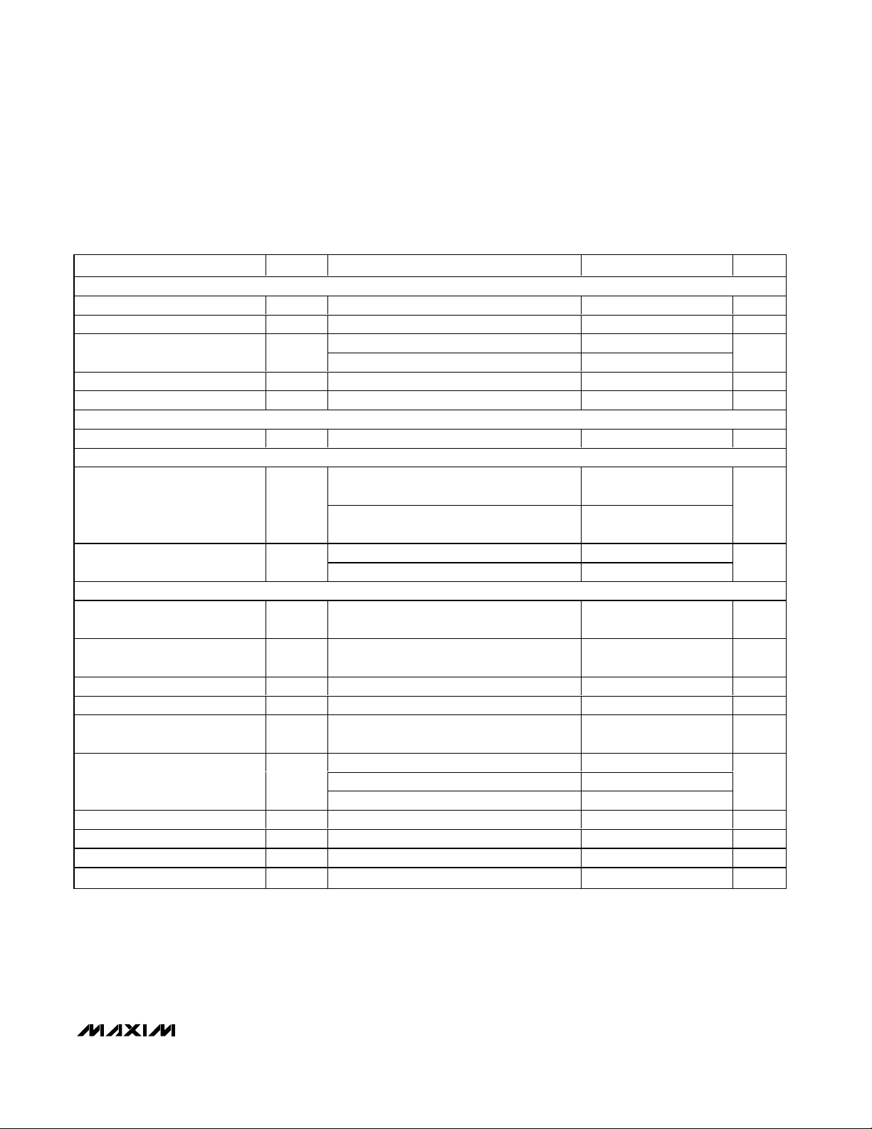
LOAD-TRANSIENT RESPONSE
(BATTERY INSERTION AND REMOVAL)
MAX1908 toc01
1ms/div
I
BATT
2A/div
V
BATT
5V/div
V
CCI
500mV/div
V
CCV
500mV/div
ICTL = LDO
VCTL = LDO
CCV
CCI
LOAD-TRANSIENT RESPONSE
(STEP IN-LOAD CURRENT)
MAX1908 toc02
1ms/div
V
BATT
2V/div
V
CCI
500mV/div
V
CCS
500mV/div
16.8V
0
0
LOAD
CURRENT
5A/div
ADAPTER
CURRENT
5A/div
ICTL = LDO
CHARGING CURRENT = 3A
V
BATT
= 16.8V
LOAD STEP = 0 TO 4A
I
SOURCE
LIMIT = 5A
CCS
CCS
CCI
CCI
V
BATT
2V/div
0
0
0
CHARGE
CURRENT
2A/div
LOAD
CURRENT
5A/div
ADAPTER
CURRENT
5A/div
LOAD-TRANSIENT RESPONSE
(STEP IN-LOAD CURRENT)
MAX1908 toc03
1ms/div
ICTL = LDO
CHARGING CURRENT = 3A
V
BATT
= 16.8V
LOAD STEP = 0 TO 4A
I
SOURCE
LIMIT = 5A
Typical Operating Characteristics
(Circuit of Figure 1, V
DCIN
= 20V, TA= +25°C, unless otherwise noted.)
0.0625
150
- 0.4V
0.250
0.2V
LDO
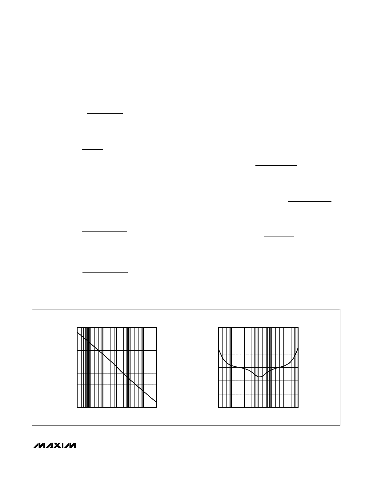
Page 11

MAX1908/MAX8724/MAX8765
Low-Cost Multichemistry Battery Chargers
______________________________________________________________________________________ 11
INDUCTOR
CURRENT
500mA/div
V
DCIN
10V/div
V
BATT
500mV/div
LINE-TRANSIENT RESPONSE
MAX1908 toc04
10ms/div
ICTL = LDO
VCTL = LDO
I
CHARGE
= 3A
LINE STEP 18.5V TO 27.5V
-1.0
-0.8
-0.9
-0.6
-0.7
-0.4
-0.5
-0.3
-0.1
-0.2
0
0 2341 567 9810
LDO LOAD REGULATION
MAX1908 toc05
LDO CURRENT (mA)
V
LDO
ERROR (%)
V
LDO
= 5.4V
-0.05
-0.03
-0.04
-0.01
-0.02
0.01
0
0.02
0.04
0.03
0.05
8 12141610 18 20 22 2624 28
LDO LINE REGULATION
MAX1908 toc06
VIN (V)
V
LDO
ERROR (%)
I
LDO
= 0
V
LDO
= 5.4V
-0.10
-0.07
-0.08
-0.09
-0.06
-0.05
-0.04
-0.03
-0.02
-0.01
0
0 200100 300 400 500
REF VOLTAGE LOAD REGULATION
MAX1908 toc07
REF CURRENT (μA)
V
REF
ERROR (%)
-0.10
-0.04
-0.06
-0.08
-0.02
0
0.02
0.04
0.06
0.08
0.10
-40 10-15 35 60 85
REF VOLTAGE ERROR vs. TEMPERATURE
MAX1908 toc08
TEMPERATURE (°C)
V
REF
ERROR (%)
90
0
0.01 1010.1
EFFICIENCY vs. CHARGE CURRENT
30
10
70
50
100
40
20
80
60
MAX1908 toc09
CHARGE CURRENT (A)
EFFICIENCY (%)
V
BATT
= 16V
V
BATT
= 8V
V
BATT
= 12V
0
100
50
250
200
150
300
350
450
400
500
0462 8 10 12 14 16 18 20 22
FREQUENCY vs. VIN - V
BATT
MAX1908 toc10
(VIN - V
BATT
) (V)
FREQUENCY (kHz)
I
CHARGE
= 3A
VCTL = ICTL = LDO
3 CELLS
4 CELLS
-0.4
-0.1
-0.3
-0.5
0
0.2
0.3
0.4
0.5
01234
OUTPUT V/I CHARACTERISTICS
MAX1908 toc11
BATT CURRENT (A)
BATT VOLTAGE ERROR (%)
0.1
-0.2
2 CELLS
3 CELLS
4 CELLS
0
0.02
0.01
0.03
0.06
0.07
0.05
0.04
0.08
0 0.2 0.3 0.4 0.50.1 0.6 0.7 0.8 0.9
1.0
BATT VOLTAGE ERROR vs. VCTL
MAX1908 toc12
VCTL/REFIN (%)
BATT VOLTAGE ERROR (%)
4 CELLS
REFIN = 3.3V
NO LOAD
Typical Operating Characteristics (continued)
(Circuit of Figure 1, V
DCIN
= 20V, TA= +25°C, unless otherwise noted.)
Page 12

MAX1908/MAX8724/MAX8765
Low-Cost Multichemistry Battery Chargers
12 ______________________________________________________________________________________
-1
1
0
3
2
4
5
01.00.5 1.5 2.0
CURRENT-SETTING ERROR vs. ICTL
MAX1908 toc13
V
ICTL
(V)
CURRENT-SETTING ERROR (%)
V
REFIN
= 3.3V
0
1.5
1.0
0.5
2.0
2.5
3.0
3.5
4.0
4.5
5.0
01.00.5 1.5 2.0 2.5 3.0
ICHG ERROR vs. CHARGE CURRENT
MAX1908 toc14
I
BATT
(A)
ICHG (%)
V
BATT
= 16V
V
BATT
= 12V
V
BATT
= 8V
V
REFIN
= 3.3V
-40
-30
-20
-10
0
10
20
30
40
01234
IINP ERROR vs. SYSTEM LOAD CURRENT
MAX1908 toc15
SYSTEM LOAD CURRENT (A)
IINP ERROR (%)
I
BATT
= 0
-80
-60
-40
-20
0
20
40
60
80
0 0.5 1.0 1.5 2.0
IINP ERROR vs. INPUT CURRENT
MAX1908 toc16
INPUT CURRENT (A)
IINP ERROR (%)
SYSTEM LOAD = 0
ERROR DUE TO SWITCHING NOISE
Typical Operating Characteristics (continued)
(Circuit of Figure 1, V
DCIN
= 20V, TA= +25°C, unless otherwise noted.)
Page 13

MAX1908/MAX8724/MAX8765
Low-Cost Multichemistry Battery Chargers
______________________________________________________________________________________ 13
Pin Description
PIN
NAME
FUNCTION
1
Charging Voltage Input. Bypass DCIN with a 1µF capacitor to PGND.
2 LDO D evi ce P ow er S up p l y. Outp ut of the 5.4V l i near r eg ul ator sup p l i ed fr om D C IN . Byp a ss w i th a 1µF cap aci tor to GN D .
3 CLS Source Current-Limit Input. Voltage input for setting the current limit of the input source.
4 REF 4.096V Voltage Reference. Bypass REF with a 1µF capacitor to GND.
5 CCS Input-Current Regulation Loop-Compensation Point. Connect a 0.01µF capacitor to GND.
6 CCI Output-Current Regulation Loop-Compensation Point. Connect a 0.01µF capacitor to GND.
7 CCV Voltage Regulation Loop-Compensation Point. Connect 1kΩ in series with a 0.1µF capacitor to GND.
8
Shutdown Control Input. Drive SHDN logic low to shut down the MAX1908/MAX8724/MAX8765. Use with a
thermistor to detect a hot battery and suspend charging.
9
Charge-Current Monitor Output. ICHG is a scaled-down replica of the charger output current. Use ICHG to
monitor the charging current and detect when the chip changes from constant-current mode to constant-
voltage mode. The transconductance of (CSIP - CSIN) to ICHG is 3µA/mV.
10 ACIN AC Detect Input. Input to an uncommitted comparator. ACIN can be used to detect AC-adapter presence.
11
AC Detect Output. High-voltage open-drain output is high impedance when V
ACIN
is less than V
REF
/ 2.
12
Reference Input. Allows the ICTL and VCTL inputs to have ratiometric ranges for increased accuracy.
13 ICTL
Output Current-Limit Set Input. ICTL input voltage range is V
REFIN
/ 32 to V
REFIN
. The MAX1908/MAX8724
shut down if ICTL is forced below V
REFIN
/ 100 while the MAX8765 does not. When ICTL is equal to LDO, the
set point for CSIP - CSIN is 45mV.
14 GND Analog Ground
15
Output Voltage-Limit Set Input. VCTL input voltage range is 0 to V
REFIN
. When VCTL is equal to LDO, the set
point is (4.2 x CELLS)V.
16
Battery Voltage Input
17
Cell Count Input. Tri-level input for setting number of cells. GND = 2 cells, float = 3 cells, REFIN = 4 cells.
18 CSIN Output Current-Sense Negative Input
19 CSIP Output Current-Sense Positive Input. Connect a current-sense resistor from CSIP to CSIN.
20
Power Ground
21 DLO Low-Side Power MOSFET Driver Output. Connect to low-side nMOS gate.
22
Low-Side Driver Supply. Bypass DLOV with a 1µF capacitor to GND.
23 LX High-Side Power MOSFET Driver Power-Return Connection. Connect to the source of the high-side nMOS.
24 BST High-Side Power MOSFET Driver Power-Supply Connection. Connect a 0.1µF capacitor from LX to BST.
25 DHI High-Side Power MOSFET Driver Output. Connect to high-side nMOS gate.
26
Input Current-Sense Negative Input
27
Input Current-Sense Positive Input. Connect a current-sense resistor from CSSP to CSSN.
28 IINP
Input-Current Monitor Output. IINP is a scaled-down replica of the input current. IINP monitors the total
system current. The transconductance of (CSSP - CSSN) to IINP is 3µA/mV.
DCIN
SHDN
ICHG
ACOK
REFIN
VCTL
BATT
CELLS
PGND
DLOV
CSSN
CSSP
Page 14

Low-Cost Multichemistry Battery Chargers
14 ______________________________________________________________________________________
MAX1908/MAX8724/MAX8765
Detailed Description
The MAX1908/MAX8724/MAX8765 include all the functions necessary to charge Li+ batteries. A high-efficiency synchronous-rectified step-down DC-DC converter
controls charging voltage and current. The device also
includes input-source current limiting and analog inputs
for setting the charge current and charge voltage.
Control charge current and voltage using the ICTL and
VCTL inputs, respectively. Both ICTL and VCTL are
ratiometric with respect to REFIN, allowing compatibility
with DACs or microcontrollers (µCs). Ratiometric ICTL
and VCTL improve the accuracy of the charge current
and voltage set point by matching V
REFIN
to the reference of the host. For standard applications, internal set
points for ICTL and VCTL provide 3A charge current
(with 0.015Ω sense resistor), and 4.2V (per cell) charge
voltage. Connect ICTL and VCTL to LDO to select the
internal set points. The MAX1908 safely conditions
overdischarged cells with 300mA (with 0.015Ω sense
resistor) until the battery-pack voltage exceeds 3.1V ×
number of series-connected cells. The SHDN input
allows shutdown from a microcontroller or thermistor.
The DC-DC converter uses external n-channel
MOSFETs as the buck switch and synchronous rectifier
to convert the input voltage to the required charging
current and voltage. The Typical Application Circuit
shown in Figure 1 uses a µC to control charging current, while Figure 2 shows a typical application with
charging voltage and current fixed to specific values
for the application. The voltage at ICTL and the value of
RS2 set the charging current. The DC-DC converter
generates the control signals for the external MOSFETs
to regulate the voltage and the current set by the VCTL,
ICTL, and CELLS inputs.
The MAX1908/MAX8724/MAX8765 feature a voltage
regulation loop (CCV) and two current regulation loops
(CCI and CCS). The CCV voltage regulation loop monitors BATT to ensure that its voltage does not exceed
the voltage set by VCTL. The CCI battery current regulation loop monitors current delivered to BATT to ensure
that it does not exceed the current limit set by ICTL. A
third loop (CCS) takes control and reduces the batterycharging current when the sum of the system load and
the battery-charging input current exceeds the input
current limit set by CLS.
Setting the Battery-Regulation Voltage
The MAX1908/MAX8724/MAX8765 use a high-accuracy
voltage regulator for charging voltage. The VCTL input
adjusts the charger output voltage. VCTL control voltage can vary from 0 to V
REFIN
, providing a 10% adjust-
ment range on the V
BATT
regulation voltage. By limiting
the adjust range to 10% of the regulation voltage, the
external resistor mismatch error is reduced from 1% to
0.05% of the regulation voltage. Therefore, an overall
voltage accuracy of better than 0.7% is maintained
while using 1% resistors. The per-cell battery termination voltage is a function of the battery chemistry.
Consult the battery manufacturer to determine this voltage. Connect VCTL to LDO to select the internal default
setting V
BATT
= 4.2V × number of cells, or program the
battery voltage with the following equation:
CELLS is the programming input for selecting cell count.
Connect CELLS as shown in Table 2 to charge 2, 3, or 4
Li+ cells. When charging other cell chemistries, use
CELLS to select an output voltage range for the charger.
The internal error amplifier (GMV) maintains voltage
regulation (Figure 3). The voltage error amplifier is
compensated at CCV. The component values shown in
Figures 1 and 2 provide suitable performance for most
applications. Individual compensation of the voltage regulation and current regulation loops allows for optimal
compensation (see the Compensation section).
V CELLS V
V
V
BATT
VCTL
REFIN
=×+×
⎛
⎝
⎜
⎞
⎠
⎟
⎛
⎝
⎜
⎞
⎠
⎟
404.
Table 2. Cell-Count Programming
DESCRIPTION
MAX1908
MAX8724
MAX8765
Conditioning
Charge Feature
Yes No No
ICTL Shutdown
Mode
Yes Yes No
ACOK Enable
Condition
REFIN must
be ready
REFIN must
be ready
Independent
of REFIN
Table 1. Versions Comparison
CELLS CELL COUNT
GND 2
Float 3
V
REFIN
4
Page 15

MAX1908/MAX8724
Low-Cost Multichemistry Battery Chargers
______________________________________________________________________________________ 15
MAX1908/MAX8724/MAX8765
DCIN
LDO
MAX1908
MAX8724
MAX8765
CLSREF
GND
CELLS
DLOV
AC ADAPTER INPUT
8.5V TO 28V
12.6V OUTPUT VOLTAGE
7.5A INPUT
CURRENT LIMIT
DHI
D3
BST
SMART
BATTERY
HOST
ACIN
D2
R6
59kΩ
1%
R7
19.6kΩ
1%
C5
1μF
VCTL
ICTL
REFIN
ACOK
ICHG
IINP
R8
1MΩ
R9
20kΩ
R10
10kΩ
C14
0.1μF
C20
0.1μF
CCV
C11
0.1μF
R5
1kΩ
CCI
CCS
C10
0.01μF
C9
0.01μF
C12
1μF
C1
2 × 10μF
C13
1μF
C15
0.1μF
LX
C16
1μF
LDO
R13
33Ω
CSSP CSSN
FLOAT (3 CELLS SELECT)
D1
RS1
0.01Ω
L1
10μH
RS2
0.015Ω
CSIP
CSIN
PGND
DLO
N1b
N1a
BATT
C4
22μF
BATT
+
R19, R20, R21
10kΩ
AVDD/REF
SCL
SDA
TEMP
BATT-
ADC INPUT
ADC INPUT
OUTPUT
DAC OUTPUT
V
CC
SCL
SDA
ADC INPUT
GND
PGND GND
TO EXTERNAL
LOAD
SHDN
0.1μF
0.1μF
Figure 1. µC-Controlled Typical Application Circuit
Typical Application Circuits
Page 16

Low-Cost Multichemistry Battery Chargers
16 ______________________________________________________________________________________
MAX1908/MAX8724/MAX8765
TO EXTERNAL
LOAD
MAX1908
MAX8724
MAX8765
CLSREF
GND
CELLS
REFIN (4 CELLS SELECT)
DLOV
AC ADAPTER
INPUT
8.5V TO 28V
DHI
D3
BST
BATTERY
ACIN
D2
LDO
LDO
16.8V OUTPUT VOLTAGE
2.5A CHARGE LIMIT
4A INPUT CURRENT LIMIT
R6
59kΩ
1%
R7
19.6kΩ
1%
R11
15kΩ
R12
12kΩ
C5
1μF
C12
1.5nF
SHDN
ICHG
IINP
R19
10kΩ
1%
R20
10kΩ
1%
CCV
C11
0.1μF
R5
1kΩ
CCI
CCS
C10
0.01μF
C9
0.01μF
C12
1μF
C1
2 × 10μF
C13
1μF
C15
0.1μF
LX
C16
1μF
LDO
R13
33Ω
CSSP CSSN
RS1
0.01Ω
L1
10μH
RS2
0.015Ω
CSIP
CSIN
PGND
DLO
N1b
N1a
FROM HOST μP
(SHUTDOWN)
N
BATT
GNDPGND
C4
22μF
BATT
+
REFIN
VCTL
DCIN
BATT-
THM
ICTL
R14
10.5kΩ
1%
R15
8.25kΩ
1%
R16
8.25kΩ
1%
P1
R17
19.1kΩ
1%
R18
22kΩ
1%
ACOK
0.01μF
0.01μF
Figure 2. Typical Application Circuit with Fixed Charging Parameters
Typical Application Circuits (continued)
Page 17

MAX1908/MAX8724
Low-Cost Multichemistry Battery Chargers
______________________________________________________________________________________ 17
MAX1908/MAX8724/MAX8765
MAX1908
MAX8724
MAX8765
LOGIC
BLOCK
GMS
SHDN
GND
CLS
CCS
CSSP
CSSN
CSIP
CSIN
ICTL
CCI
BATT
CELLS
CCV
VCTL
23.5%
REFIN
GND
DCIN
SRDY
5.4V
LINEAR
REGULATOR
1/55
ICTL
MAX1908/MAX8724 ONLY
REF/2
RDY
4V
CELL
SELECT
LOGIC
4.096V
REFERENCE
LVC
REFIN
CSI
BAT_UV
3.1V/CELL
R1
LVC
DCIN
LDO
REF
REFIN
ACIN
ACOK
IINP
ICHG
BST
DHI
LX
DLOV
DLO
PGND
MAX1908 ONLY
x
75mV
REF
LEVEL
SHIFTER
x
75mV
REFIN
x
400mV
REFIN
DC-DC
CONVERTER
GMI
GMV
GM
LEVEL
SHIFTER
N
GM
LEVEL
SHIFTER
DRIVER
DRIVER
Figure 3. Functional Diagram
Functional Diagram
Page 18

Low-Cost Multichemistry Battery Chargers
18 ______________________________________________________________________________________
MAX1908/MAX8724/MAX8765
Setting the Charging-Current Limit
The ICTL input sets the maximum charging current. The
current is set by current-sense resistor RS2, connected
between CSIP and CSIN. The full-scale differential
voltage between CSIP and CSIN is 75mV; thus, for a
0.015Ω sense resistor, the maximum charging current
is 5A. Battery-charging current is programmed with
ICTL using the equation:
The input voltage range for ICTL is V
REFIN
/ 32 to
V
REFIN
. The MAX1908/MAX8724 shut down if ICTL is
forced below V
REFIN
/ 100 (min), while the MAX8765
does not.
Connect ICTL to LDO to select the internal default fullscale, charge-current sense voltage of 45mV. The
charge current when ICTL = LDO is:
where RS2 is 0.015Ω, providing a charge-current set
point of 3A.
The current at the ICHG output is a scaled-down replica
of the battery output current being sensed across CSIP
and CSIN (see the Current Measurement section).
When choosing the current-sense resistor, note that the
voltage drop across this resistor causes further power
loss, reducing efficiency. However, adjusting ICTL to
reduce the voltage across the current-sense resistor
can degrade accuracy due to the smaller signal to the
input of the current-sense amplifier. The chargingcurrent-error amplifier (GMI) is compensated at CCI
(see the Compensation section).
Setting the Input Current Limit
The total input current (from an AC adapter or other DC
source) is a function of the system supply current and
the battery-charging current. The input current regulator
limits the input current by reducing the charging
current when the input current exceeds the input
current-limit set point. System current normally fluctuates as portions of the system are powered up or
down. Without input current regulation, the source must
be able to supply the maximum system current and the
maximum charger input current simultaneously. By using
the input current limiter, the current capability of the AC
adapter can be lowered, reducing system cost.
The MAX1908/MAX8724/MAX8765 limit the battery
charge current when the input current-limit threshold is
exceeded, ensuring the battery charger does not load
down the AC adapter voltage. An internal amplifier
compares the voltage between CSSP and CSSN to the
voltage at CLS. V
CLS
can be set by a resistive divider
between REF and GND. Connect CLS to REF for the
full-scale input current limit. The CLS voltage range for
the MAX1908/MAX8724 is from 1.6V to REF, while the
MAX8765 CLS voltage is from 1.1V to REF.
The input current is the sum of the device current, the
charger input current, and the load current. The device
current is minimal (3.8mA) in comparison to the charge
and load currents. Determine the actual input current
required as follows:
where η is the efficiency of the DC-DC converter.
V
CLS
determines the reference voltage of the GMS
error amplifier. Sense resistor RS1 and V
CLS
determine
the maximum allowable input current. Calculate the
input current limit as follows:
Once the input current limit is reached, the charging
current is reduced until the input current is at the
desired threshold.
When choosing the current-sense resistor, note that the
voltage drop across this resistor causes further power
loss, reducing efficiency. Choose the smallest value for
RS1 that achieves the accuracy requirement for the
input current-limit set point.
Conditioning Charge
The MAX1908 includes a battery-voltage comparator
that allows a conditioning charge of overdischarged
Li+ battery packs. If the battery-pack voltage is less
than 3.1V × number of cells programmed by CELLS,
the MAX1908 charges the battery with 300mA current
when using sense resistor RS2 = 0.015Ω. After the
battery voltage exceeds the conditioning charge
threshold, the MAX1908 resumes full-charge mode,
charging to the programmed voltage and current limits.
The MAX8724/MAX8765 do not offer this feature.
AC Adapter Detection
Connect the AC adapter voltage through a resistive
divider to ACIN to detect when AC power is available,
as shown in Figure 1. ACIN voltage rising trip point is
V
REF
/ 2 with 20mV hysteresis. ACOK is an open-drain
output and is high impedance when ACIN is less than
V
REF
/ 2. Since ACOK can withstand 30V (max), ACOK
I
V
VRS
INPUT
CLS
REF
=×
0 0751.
II
IV
V
INPUT LOAD
CHG BATT
IN
=+
×
×
⎛
⎝
⎜
⎞
⎠
⎟
η
I
V
RS
CHG
=
0 0452.
I
V
VRS
CHG
ICTL
REFIN
=×
0 0752.
Page 19

MAX1908/MAX8724
Low-Cost Multichemistry Battery Chargers
______________________________________________________________________________________ 19
can drive a p-channel MOSFET directly at the charger
input, providing a lower dropout voltage than a
Schottky diode (Figure 2). In the MAX1908/MAX8724
the ACOK comparator is enabled after REFIN is ready.
In the MAX8765, the ACOK comparator is independent
of REFIN.
Current Measurement
Use ICHG to monitor the battery-charging current being
sensed across CSIP and CSIN. The ICHG voltage is
proportional to the output current by the equation:
V
ICHG
= ICHG x RS2 x G
ICHG
x R9
where I
CHG
is the battery-charging current, G
ICHG
is
the transconductance of ICHG (3µA/mV typ), and R9 is
the resistor connected between ICHG and ground.
Leave ICHG unconnected if not used.
Use IINP to monitor the system input current being
sensed across CSSP and CSSN. The voltage of IINP is
proportional to the input current by the equation:
V
IINP
= I
INPUT
x RS1 x G
IINP
x R10
where I
INPUT
is the DC current being supplied by the AC
adapter power, G
IINP
is the transconductance of IINP
(3µA/mV typ), and R10 is the resistor connected between
IINP and ground. ICHG and IINP have a 0 to 3.5V output
voltage range. Leave IINP unconnected if not used.
LDO Regulator
LDO provides a 5.4V supply derived from DCIN and
can deliver up to 10mA of load current. The MOSFET
drivers are powered by DLOV and BST, which must be
connected to LDO as shown in Figure 1. LDO supplies
the 4.096V reference (REF) and most of the control circuitry. Bypass LDO with a 1µF capacitor to GND.
Shutdown
The MAX1908/MAX8724/MAX8765 feature a low-power
shutdown mode. Driving SHDN low shuts down the
MAX1908/MAX8724/MAX8765. In shutdown, the DCDC converter is disabled and CCI, CCS, and CCV are
pulled to ground. The IINP and ACOK outputs continue
to function.
SHDN can be driven by a thermistor to allow automatic
shutdown of the MAX1908/MAX8724/MAX8765 when
the battery pack is hot. The shutdown falling threshold
is 23.5% (typ) of V
REFIN
with 1% V
REFIN
hysteresis to
provide smooth shutdown when driven by a thermistor.
DC-DC Converter
The MAX1908/MAX8724/MAX8765 employ a buck regulator with a bootstrapped nMOS high-side switch and
a low-side nMOS synchronous rectifier.
CCV, CCI, CCS, and LVC Control Blocks
The MAX1908/MAX8724/MAX8765 control input current
(CCS control loop), charge current (CCI control loop),
or charge voltage (CCV control loop), depending on
the operating condition.
The three control loops, CCV, CCI, and CCS are brought
together internally at the LVC amplifier (lowest voltage
clamp). The output of the LVC amplifier is the feedback
control signal for the DC-DC controller. The output of the
G
M
amplifier that is the lowest sets the output of the LVC
amplifier and also clamps the other two control loops to
within 0.3V above the control point. Clamping the other
two control loops close to the lowest control loop ensures
fast transition with minimal overshoot when switching
between different control loops.
DC-DC Controller
The MAX1908/MAX8724/MAX8765 feature a variable offtime, cycle-by-cycle current-mode control scheme.
Depending upon the conditions, the MAX1908/MAX8724/
MAX8765 work in continuous or discontinuous-conduction mode.
Continuous-Conduction Mode
With sufficient charger loading, the MAX1908/MAX8724/
MAX8765 operate in continuous-conduction mode
(inductor current never reaches zero) switching at
400kHz if the BATT voltage is within the following range:
3.1V x (number of cells) < V
BATT
< (0.88 x V
DCIN
)
The operation of the DC-DC controller is controlled by
the following four comparators as shown in Figure 4:
• IMIN—Compares the control point (LVC) against
0.15V (typ). If IMIN output is low, then a new cycle
cannot begin.
• CCMP—Compares the control point (LVC) against the
charging current (CSI). The high-side MOSFET ontime is terminated if the CCMP output is high.
• IMAX—Compares the charging current (CSI) to 6A
(RS2 = 0.015Ω). The high-side MOSFET on-time is
terminated if the IMAX output is high and a new cycle
cannot begin until IMAX goes low.
• ZCMP—Compares the charging current (CSI) to
333mA (RS2 = 0.015Ω). If ZCMP output is high, then
both MOSFETs are turned off.
MAX1908/MAX8724/MAX8765
Page 20

Low-Cost Multichemistry Battery Chargers
20 ______________________________________________________________________________________
MAX1908/MAX8724/MAX8765
IMAX
RESET
1.8V
0.15V
0.1V
5ms
LVC
CONTROL
CELLS
SETV
SETI
CCVCCICCS
GMS
GMI
GMV
CLS
DLO
DHI
CSI
X20
t
OFF
GENERATOR
BST
S
RQ
CCMP
ZCMP
IMIN
CHG
RQ
S
CSS
X20
CSSP
AC ADAPTER
CSSN
BST
DHI
LX
RS1
LDO
D3
N1a
N1b
C
BST
L1
RS2
DLO
CSIP
CSIN
C
OUT
BATT
BATTERY
MAX1908
MAX8724
MAX8765
Q
CELL
SELECT
LOGIC
Figure 4. DC-DC Functional Diagram
DC-DC Functional Diagram
Page 21

MAX1908/MAX8724
Low-Cost Multichemistry Battery Chargers
______________________________________________________________________________________ 21
In normal operation, the controller starts a new cycle by
turning on the high-side n-channel MOSFET and
turning off the low-side n-channel MOSFET. When the
charge current is greater than the control point (LVC),
CCMP goes high and the off-time is started. The
off-time turns off the high-side n-channel MOSFET and
turns on the low-side n-channel MOSFET. The operational frequency is governed by the off-time and is
dependent upon V
DCIN
and V
BATT
. The off-time is set
by the following equations:
where:
These equations result in fixed-frequency operation
over the most common operating conditions.
At the end of the fixed off-time, another cycle begins if
the control point (LVC) is greater than 0.15V, IMIN =
high, and the peak charge current is less than 6A (RS2
= 0.015Ω), IMAX = high. If the charge current exceeds
IMAX, the on-time is terminated by the IMAX comparator. IMAX governs the maximum cycle-by-cycle current
limit and is internally set to 6A (RS2 = 0.015Ω). IMAX
protects against sudden overcurrent faults.
If, during the off-time, the inductor current goes to zero,
ZCMP = high, both the high- and low-side MOSFETs
are turned off until another cycle is ready to begin.
There is a minimum 0.3µs off-time when the (V
DCIN
-
V
BATT
) differential becomes too small. If V
BATT
≥ 0.88 ×
V
DCIN
, then the threshold for minimum off-time is
reached and the t
OFF
is fixed at 0.3µs. A maximum ontime of 5ms allows the controller to achieve > 99% duty
cycle in continuous-conduction mode. The switching
frequency in this mode varies according to the equation:
Discontinuous Conduction
The MAX1908/MAX8724/MAX8765 enter discontinuousconduction mode when the output of the LVC control
point falls below 0.15V. For RS2 = 0.015Ω, this corresponds to 0.5A:
for RS2 = 0.015Ω.
In discontinuous mode, a new cycle is not started until
the LVC voltage rises above 0.15V. Discontinuousmode operation can occur during conditioning charge
of overdischarged battery packs, when the charge current has been reduced sufficiently by the CCS control
loop, or when the battery pack is near full charge (constant-voltage-charging mode).
MOSFET Drivers
The low-side driver output DLO switches between
PGND and DLOV. DLOV is usually connected through
a filter to LDO. The high-side driver output DHI is bootstrapped off LX and switches between VLXand V
BST
.
When the low-side driver turns on, BST rises to one
diode voltage below DLOV.
Filter DLOV with a lowpass filter whose cutoff frequency
is approximately 5kHz (Figure 1):
Dropout Operation
The MAX1908/MAX8724/MAX8765 have 99% duty-cycle
capability with a 5ms (max) on-time and 0.3µs (min) offtime. This allows the charger to achieve dropout performance limited only by resistive losses in the DC-DC
converter components (D1, N1, RS1, and RS2, Figure 1).
Replacing diode D1 with a p-channel MOSFET driven by
ACOK improves dropout performance (Figure 2). The
dropout voltage is set by the difference between DCIN
and CSIN. When the dropout voltage falls below 100mV,
the charger is disabled; 200mV hysteresis ensures that
the charger does not turn back on until the dropout voltage rises to 300mV.
Compensation
Each of the three regulation loops—input current limit,
charging current limit, and charging voltage limit—are
compensated separately using CCS, CCI, and CCV,
respectively.
f
RC F
kHz
C
==
××
=
1
2
1
2331
48
ππ μΩ
.
IMIN
V
RSA=×
=
015
20 2
05..
f
LI
VV
s
RIPPLE
CSSN BATT
=
×
−
()
+103. μ
f
tt
ON OFF
=
+
1
I
Vt
L
RIPPLE
BATT OFF
=
×
t
LI
VV
ON
RIPPLE
CSSN BATT
=
×
−
ts
VV
V
OFF
DCIN BATT
DCIN
=×
−
25. μ
MAX1908/MAX8724/MAX8765
Page 22

Low-Cost Multichemistry Battery Chargers
22 ______________________________________________________________________________________
MAX1908/MAX8724/MAX8765
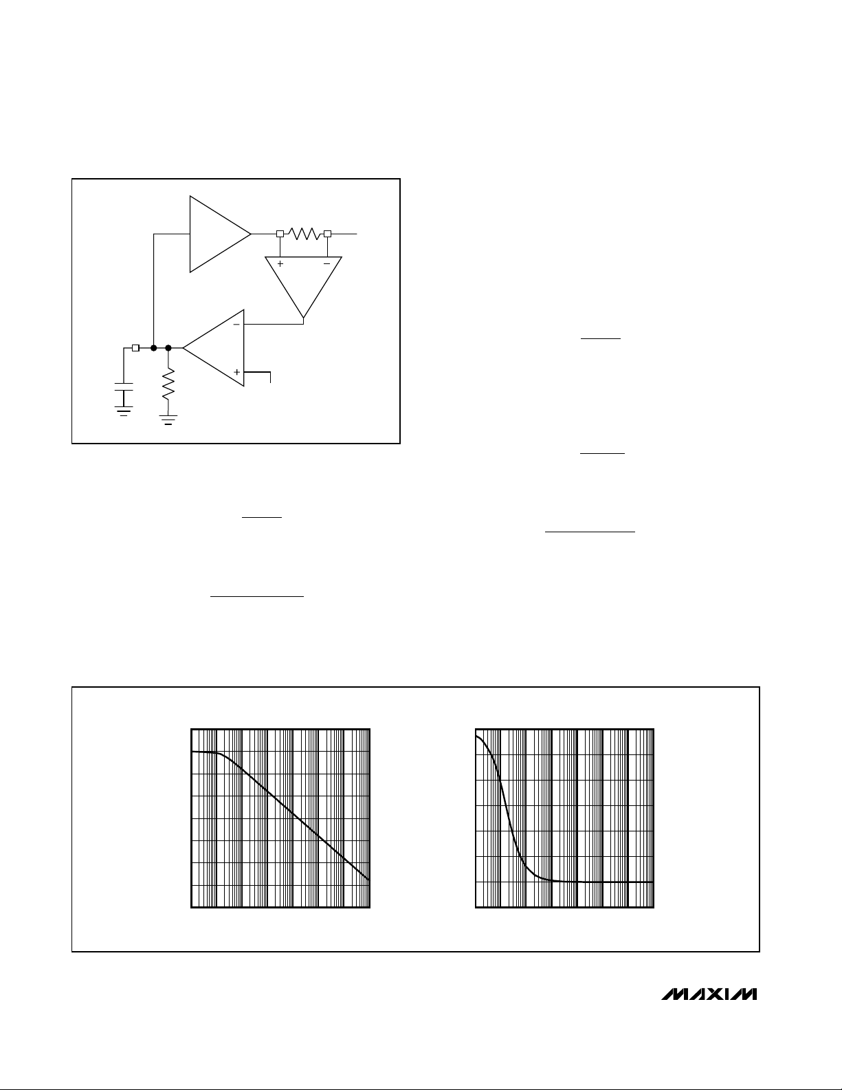
CCV Loop Definitions
Compensation of the CCV loop depends on the parameters and components shown in Figure 5. CCVand
RCVare the CCV loop compensation capacitor and
series resistor. R
ESR
is the equivalent series resistance
(ESR) of the charger output capacitor (C
OUT
). RLis the
equivalent charger output load, where RL= V
BATT
/
I
CHG
. The equivalent output impedance of the GMV
amplifier, R
OGMV
≥ 10MΩ. The voltage amplifier
transconductance, GMV = 0.125µA/mV. The DC-DC
converter transconductance, GM
OUT
= 3.33A/V:
where A
CSI
= 20, and RS2 is the charging current-
sense resistor in the Typical Application Circuits.
The compensation pole is given by:
The compensation zero is given by:
The output pole is given by:
where RLvaries with load according to RL= V
BATT
/ I
CHG.
Output zero due to output capacitor ESR:
The loop transfer function is given by:
Assuming the compensation pole is a very low
frequency, and the output zero is a much higher frequency, the crossover frequency is given by:
To calculate RCVand CCVvalues of the circuit of Figure 2:
Cells = 4
C
OUT
= 22µF
V
BATT
= 16.8V
I
CHG
= 2.5A
GMV = 0.125µA/mV
GM
OUT
= 3.33A/V
R
OGMV
= 10MΩ
f = 400kHz
Choose crossover frequency to be 1/5th the
MAX1908’s 400kHz switching frequency:
Solving yields R
CV
= 26kΩ.
Conservatively set RCV= 1kΩ, which sets the crossover
frequency at:
f
CO_CV
= 3kHz
Choose the output-capacitor ESR so the output-capacitor
zero is 10 times the crossover frequency:
f
RC
MHz
Z ESR
ESR OUT
_
.=
×
=
1
2
2 412
π
R
fC
ESR
CO CV OUT
=
×× ×
=
1
210
024
π
_
. Ω
f
GMV R GM
C
kHz
CO CV
CV OUT
OUT
_
=
××
=280
π
f
GMV R GM
C
CO CV
CV OUT
OUT
_
=
××
2π
LTF GM R GMV R
sC R sC R
sC R sC R
OUT L OGMV
OUT ESR CV CV
CV OGMV OUT L
=××××
+×
()
+×
()
+×
()
+×
()
11
11
f
RC
Z ESR
ESR OUT
_
=
×
1
2π
f
RC
P OUT
L OUT
_
=
×
1
2πfRC
ZCV
CV CV
_
=
×
1
2π
f
RC
PCV
OGMV CV
_
=
×
1
2πGMARS
OUT
CSI
=
×12
GM
OUT
BATT
CCV
GMV
REF
R
CV
C
CV
R
OGMV
R
ESR
R
L
C
OUT
Figure 5. CCV Loop Diagram
Page 23
MAX1908/MAX8724
Low-Cost Multichemistry Battery Chargers
______________________________________________________________________________________ 23
The 22µF ceramic capacitor has a typical ESR of
0.003Ω, which sets the output zero at 2.412MHz.
The output pole is set at:
where:
Set the compensation zero (f
Z_CV
) so it is equivalent to
the output pole (f
P_OUT
= 1.08kHz), effectively producing a pole-zero cancellation and maintaining a singlepole system response:
Choose CCV= 100nF, which sets the compensation
zero (f
Z_CV
) at 1.6kHz. This sets the compensation pole:
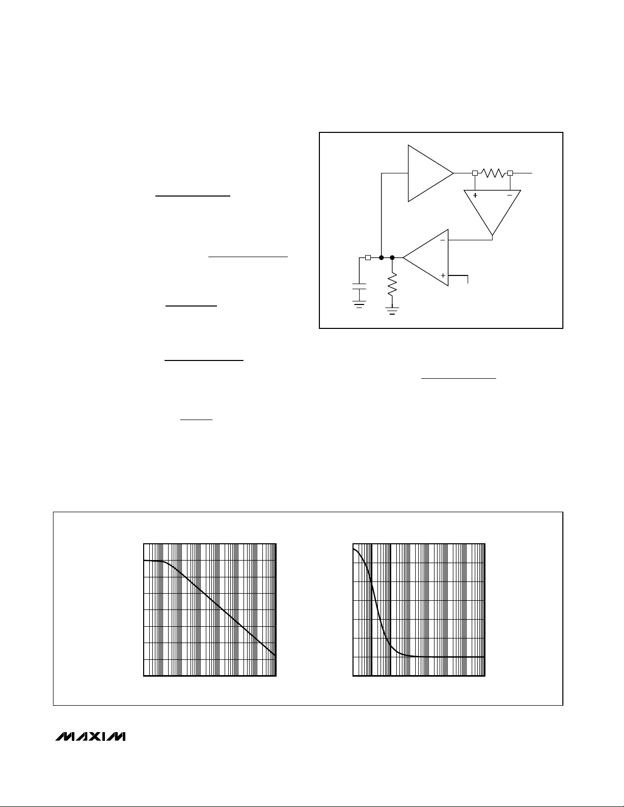
CCI Loop Definitions
Compensation of the CCI loop depends on the parameters and components shown in Figure 7. CCIis the CCI
loop compensation capacitor. A
CSI
is the internal gain
of the current-sense amplifier. RS2 is the charge current-sense resistor, RS2 = 15mΩ. R
OGMI
is the equiva-
lent output impedance of the GMI amplifier ≥ 10MΩ.
GMI is the charge-current amplifier transconductance
= 1µA/mV. GM
OUT
is the DC-DC converter transconductance = 3.3A/V. The CCI loop is a single-pole system with a dominant pole compensation set by f
P_CI
:
The loop transfer function is given by:
Since:
The loop transfer function simplifies to:
LTF GMI
R
sR C
OGMI
OGMI CI
=×
+×1
GM
ARS
OUT
CSI
=
×12
LTF GM A RS GMI
R
sR C
OUT CSI
OGMI
OGMI CI
=×××
+×
2
1
f
RC
PCI
OGMI CI
_
=
×
1
2π
f
RC
Hz
PCV
OGMV CV
_
.=
×
=
1
2
016
π
C
R kHz
nF
CV
CV
=
×
=
1
2108
147
π .
f
RC
ZCV
CV CV
_
=
×
1
2π
R
V
I
Battery ESR
L
BATT
CHG
==
Δ
Δ
f
RC
kHz
P OUT
L OUT
_
.=
×
=
1
2
108
π
MAX1908/MAX8724/MAX8765
CCV LOOP GAIN
vs. FREQUENCY
FREQUENCY (Hz)
GAIN (dB)
100k10k1k10010
-40
-20
0
20
40
60
80
-60
11M
CCV LOOP PHASE
vs. FREQUENCY
FREQUENCY (Hz)
PHASE (DEGREES)
100k10k1k10010
-120
-105
-90
-75
-60
-45
-135
11M
Figure 6. CCV Loop Gain/Phase vs. Frequency
Page 24
Low-Cost Multichemistry Battery Chargers
24 ______________________________________________________________________________________
MAX1908/MAX8724/MAX8765
The crossover frequency is given by:
The CCI loop dominant compensation pole:
where the GMI amplifier output impedance, R
OGMI
=
10MΩ.
To calculate the CCI loop compensation pole, C
CI
:
GMI = 1µA/mV
GM
OUT
= 3.33A/V
R
OGMI
= 10MΩ
f = 400kHz
Choose crossover frequency f
CO_
CI
to be 1/5th the
MAX1908/MAX8724/MAX8765 switching frequency:
Solving for CCI, CCI= 2nF.
To be conservative, set CCI= 10nF, which sets the
crossover frequency at:
The compensation pole, f
P_CI
is set at:
CCS Loop Definitions
Compensation of the CCS loop depends on the parameters and components shown in Figure 9. CCSis the CCS
loop compensation capacitor. A
CSS
is the internal gain of
the current-sense amplifier. RS1 is the input currentsense resistor, RS1 = 10mΩ. R
OGMS
is the equivalent
output impedance of the GMS amplifier ≥ 10MΩ. GMS is
f
GMI
RC
Hz
PCI
OGMI CI
_
.=
×
=20 0016
π
f
GMI
nF
kHz
CO CI_
==
210
16
π
f
GMI
C
kHz
CO CICI_
==
280π
f
RC
PCI
OGMI CI
_
=
×
1
2π
f
GMI
C
CO CICI_
=
2π
GM
OUT
CCI
GMI
ICTL
C
CI
R
OGMI
CSIP CSIN
CSI
RS2
Figure 7. CCI Loop Diagram
CCI LOOP GAIN
vs. FREQUENCY
FREQUENCY (Hz)
GAIN (dB)
100k10k1 10 100 1k
-40
-20
0
20
40
60
80
100
-60
0.1 1M
CCI LOOP PHASE
vs. FREQUENCY
FREQUENCY (Hz)
PHASE (DEGREES)
100k10k1k100101
-90
-75
-60
-45
-30
-15
0
-105
0.1 1M
Figure 8. CCI Loop Gain/Phase vs. Frequency
Page 25
MAX1908/MAX8724
Low-Cost Multichemistry Battery Chargers
______________________________________________________________________________________ 25
the charge-current amplifier transconductance = 1µA/mV.
GMINis the DC-DC converter transconductance =
3.3A/V. The CCS loop is a single-pole system with a dominant pole compensation set by f
P_CS
:
The loop transfer function is given by:
Since:
Then, the loop transfer function simplifies to:
The crossover frequency is given by:
The CCS loop dominant compensation pole:
where the GMS amplifier output impedance, R
OGMS
=
10MΩ.
To calculate the CCI loop compensation pole, CCS:
GMS = 1µA/mV
GMIN= 3.33A/V
R
OGMS
= 10MΩ
f = 400kHz
f
RC
PCS
OGMS CS
_
=
×
1
2π
f
GMS
C
CO CSCS_
=
2π
LTF GMS
R
sR C
OGMS
OGMS CS
=×
+×1
GM
ARS
IN
CSS
=
×11
LTF GM A RS GMS
R
sR C
IN CSS
OGMS
OGMS CS
=××××
+×
1
1
f
RC
PCS
OGMS CS
_
=
×
1
2π
MAX1908/MAX8724/MAX8765
GM
IN
CCS
GMS
CLS
C
CS
R
OGMS
CSSP CSSN
CSS
RS1
Figure 9. CCS Loop Diagram
CCS LOOP GAIN
vs. FREQUENCY
FREQUENCY (Hz)
GAIN (dB)
100k10k1 10 100 1k
-40
-20
0
20
40
60
80
100
-60
0.1 1M
CCS LOOP PHASE
vs. FREQUENCY
FREQUENCY (Hz)
PHASE (DEGREES)
100k10k1k100101
-90
-75
-60
-45
-30
-15
0
-105
0.1 1M
Figure 10. CCS Loop Gain/Phase vs. Frequency
Page 26

Low-Cost Multichemistry Battery Chargers
26 ______________________________________________________________________________________
MAX1908/MAX8724/MAX8765
Choose crossover frequency f
CO_CS
to be 1/5th the
MAX1908/MAX8724/MAX8765 switching frequency:
Solving for CCS, CCS= 2nF.
To be conservative, set CCS= 10nF, which sets the
crossover frequency at:
The compensation pole, f
P_CS
is set at:
Component Selection
Table 3 lists the recommended components and refers
to the circuit of Figure 2. The following sections
describe how to select these components.
Inductor Selection
Inductor L1 provides power to the battery while it is
being charged. It must have a saturation current of at
least the charge current (I
CHG
), plus 1/2 the current rip-
ple I
RIPPLE
:
I
SAT
= I
CHG
+ (1/2) I
RIPPLE
Ripple current varies according to the equation:
I
RIPPLE
= (V
BATT
) × t
OFF
/ L
where:
t
OFF
= 2.5µs × (V
DCIN
– V
BATT
) / V
DCIN
V
BATT
< 0.88 × V
DCIN
or:
t
OFF
= 0.3µs
V
BATT
> 0.88 × V
DCIN
Figure 11 illustrates the variation of ripple current vs.
battery voltage when charging at 3A with a fixed 19V
input voltage.
Higher inductor values decrease the ripple current.
Smaller inductor values require higher saturation current capabilities and degrade efficiency. Designs for
ripple current, I
RIPPLE
= 0.3 × I
CHG
usually result in a
good balance between inductor size and efficiency.
Input Capacitor
Input capacitor C1 must be able to handle the input
ripple current. At high charging currents, the DC-DC
converter operates in continuous conduction. In this
case, the ripple current of the input capacitor can be
approximated by the following equation:
where:
I
C1
= input capacitor ripple current.
D = DC-DC converter duty ratio.
I
CHG
= battery-charging current.
Input capacitor C1 must be sized to handle the maximum ripple current that occurs during continuous conduction. The maximum input ripple current occurs at
50% duty cycle; thus, the worst-case input ripple current is 0.5 × I
CHG
. If the input-to-output voltage ratio is
such that the DC-DC converter does not operate at a
50% duty cycle, then the worst-case capacitor current
occurs where the duty cycle is nearest 50%.
The input capacitor ESR times the input ripple current
sets the ripple voltage at the input, and should not
exceed 0.5V ripple. Choose the ESR of C1 according to:
The input capacitor size should allow minimal output
voltage sag at the highest switching frequency:
I
C
dV
dt
C1
2
1=
ESR
V
I
CC1
1
05<.
II DD
C CHG1
2
=−
f
RC
Hz
PCS
OGMS CS
_
.=
×
=
1
2
0 0016
π
f
GMS
nF
kHz
CO CS_
==
210
16
π
f
GMS
C
kHz
CO CSCS_
==
280π
RIPPLE CURRENT vs.
BATTERY VOLTAGE
V
BATT
(V)
RIPPLE CURRENT (A)
14131211109
0.5
1.0
1.5
0
8 15161718
V
DCIN
= 19V
VCTL = ICTL = LDO
4 CELLS
3 CELLS
Figure 11. Ripple Current vs. Battery Voltage
Page 27

MAX1908/MAX8724
Low-Cost Multichemistry Battery Chargers
______________________________________________________________________________________ 27
MAX1908/MAX8724/MAX8765
where dV is the maximum voltage sag of 0.5V while
delivering energy to the inductor during the high-side
MOSFET on-time, and dt is the period at highest operating frequency (400kHz):
Both tantalum and ceramic capacitors are suitable in
most applications. For equivalent size and voltage
rating, tantalum capacitors have higher capacitance,
but also higher ESR than ceramic capacitors. This
makes it more critical to consider ripple current and
power-dissipation ratings when using tantalum capacitors. A single ceramic capacitor often can replace two
tantalum capacitors in parallel.
Output Capacitor
The output capacitor absorbs the inductor ripple current. The output capacitor impedance must be significantly less than that of the battery to ensure that it
absorbs the ripple current. Both the capacitance and
ESR rating of the capacitor are important for its effectiveness as a filter and to ensure stability of the DC-DC
converter (see the Compensation section). Either tantalum or ceramic capacitors can be used for the output
filter capacitor.
MOSFETs and Diodes
Schottky diode D1 provides power to the load when the
AC adapter is inserted. This diode must be able to
deliver the maximum current as set by RS1. For
reduced power dissipation and improved dropout performance, replace D1 with a p-channel MOSFET (P1)
as shown in Figure 2. Take caution not to exceed the
maximum V
GS
of P1. Choose resistors R11 and R12 to
limit the VGS.
The n-channel MOSFETs (N1a, N1b) are the switching
devices for the buck controller. High-side switch N1a
should have a current rating of at least the maximum
charge current plus one-half the ripple current and
have an on-resistance (R
DS(ON)
) that meets the power
dissipation requirements of the MOSFET. The driver for
N1a is powered by BST. The gate-drive requirement for
N1a should be less than 10mA. Select a MOSFET with a
low total gate charge (Q
GATE
) and determine the
required drive current by I
GATE
= Q
GATE
× f (where f is
the DC-DC converter’s maximum switching frequency).
The low-side switch (N1b) has the same current rating
and power dissipation requirements as N1a, and
should have a total gate charge less than 10nC. N2 is
used to provide the starting charge to the BST capacitor
(C15). During the dead time (50ns, typ) between N1a
and N1b, the current is carried by the body diode of
the MOSFET. Choose N1b with either an internal
Schottky diode or body diode capable of carrying the
maximum charging current during the dead time. The
Schottky diode D3 provides the supply current to the
high-side MOSFET driver.
Layout and Bypassing
Bypass DCIN with a 1µF capacitor to power ground
(Figure 1). D2 protects the MAX1908/MAX8724/
MAX8765 when the DC power source input is reversed.
A signal diode for D2 is adequate because DCIN only
powers the internal circuitry. Bypass LDO, REF, CCV,
CCI, CCS, ICHG, and IINP to analog ground. Bypass
DLOV to power ground.
Good PC board layout is required to achieve specified
noise, efficiency, and stable performance. The PC
board layout artist must be given explicit instructions—
preferably, a pencil sketch showing the placement of
the power-switching components and high-current routing. Refer to the PC board layout in the MAX1908 evaluation kit for examples. Separate analog and power
grounds are essential for optimum performance.
Use the following step-by-step guide:
1) Place the high-power connections first, with their
grounds adjacent:
a) Minimize the current-sense resistor trace lengths,
and ensure accurate current sensing with Kelvin
connections.
b) Minimize ground trace lengths in the high-current
paths.
c) Minimize other trace lengths in the high-current
paths.
d) Use > 5mm wide traces.
e) Connect C1 to high-side MOSFET (10mm max
length).
f) LX node (MOSFETs, inductor (15mm max
length)).
Ideally, surface-mount power components are flush
against one another with their ground terminals
almost touching. These high-current grounds are
then connected to each other with a wide, filled zone
of top-layer copper, so they do not go through vias.
The resulting top-layer power ground plane is
connected to the normal ground plane at the
MAX1908/MAX8724/MAX8765s’ backside exposed
pad. Other high-current paths should also be minimized, but focusing primarily on short ground and
current-sense connections eliminates most PC
board layout problems.
C
I
s
V
C
1
22505
1
>×
..μ
Page 28

Low-Cost Multichemistry Battery Chargers
28 ______________________________________________________________________________________
MAX1908/MAX8724/MAX8765
Table 3. Component List for Circuit of Figure 2
DESIGNATION
QTY
DESCRIPTION
C1 2
10µF, 50V 2220-size ceramic
capacitors
TDK C5750X7R1H106M
C4 1
22µF, 25V 2220-size ceramic
capacitor
TDK C5750X7R1E226M
C5 1
1µF, 25V X7R ceramic capacitor
(1206)
Murata GRM31MR71E105K
Taiyo Yuden TMK316BJ105KL
TDK C3216X7R1E105K
C9, C10 2
0.01µF, 16V cer am i c cap aci tor s ( 0402)
Murata GRP155R71E103K
Taiyo Yuden EMK105BJ103KV
TDK C1005X7R1E103K
C11, C14,
C15, C20
4
0.1µF, 25V X7R ceramic capacitors
(0603)
Murata GRM188R71E104K
TDK C1608X7R1E104K
C12, C13, C16
3
1µF, 6.3V X5R ceramic capacitors
(0603)
Murata GRM188R60J105K
Taiyo Yuden JMK107BJ105KA
TDK C1608X5R1A105K
D1 (optional)
1
10A Schottky diode (D-PAK)
Diodes, Inc. MBRD1035CTL
ON Semiconductor MBRD1035CTL
D2 1
Schottky diode
Central Semiconductor
CMPSH1–4
Chip Information
TRANSISTOR COUNT: 3772
PROCESS: BiCMOS
2) Place the IC and signal components. Keep the
main switching node (LX node) away from sensitive
analog components (current-sense traces and REF
capacitor). Important: The IC must be no further
than 10mm from the current-sense resistors.
Keep the gate-drive traces (DHI, DLO, and BST)
shorter than 20mm, and route them away from the
current-sense lines and REF. Place ceramic
bypass capacitors close to the IC. The bulk capacitors can be placed further away.
3) Use a single-point star ground placed directly
below the part at the backside exposed pad of the
MAX1908/MAX8724/MAX8765. Connect the power
ground and normal ground to this node.
DESIGNATION QTY DESCRIPTION
D3 1
L1 1
N1 1
P1 1
R5 1 1kΩ ±5% resistor (0603)
R6 1 59kΩ ±1% resistor (0603)
R7 1 19.6kΩ ±1% resistor (0603)
R11 1 12kΩ ±5% resistor (0603)
R12 1 15kΩ ±5% resistor (0603)
R13 1 33Ω ±5% resistor (0603)
R14 1 10.5kΩ ±1% resistor (0603)
R15, R16 2 8.25kΩ ±1% resistors (0603)
R17 1 19.1kΩ ±1% resistor (0603)
R18 1 22kΩ ±1% resistor (0603)
R19, R20 2 10kΩ ±1% resistors (0603)
RS1 1
RS2 1
U1 1
Schottky diode
Central Semiconductor CMPSH1-4
10µH, 4.4A inductor
Sumida CDRH104R-100NC
TOKO 919AS-100M
Dual, n-channel, 8-pin SO MOSFET
Fairchild FDS6990A or FDS6990S
Single, p-channel, 8-pin SO MOSFET
Fairchild FDS6675
0.01Ω ±1%, 0.5W 2010 sense resistor
Vishay Dale WSL2010 0.010 1.0%
IRC LRC-LR2010-01-R010-F
0.015Ω ±1%, 0.5W 2010 sense
resistor
Vishay Dale WSL2010 0.015 1.0%
IRC LRC-LR2010-01-R015-F
MAX1908ETI, MAX8724ETI, or
MAX8765ETI
Page 29

MAX1908/MAX8724
Low-Cost Multichemistry Battery Chargers
MAX1908/MAX8724/MAX8765
Maxim cannot assume responsibility for use of any circuitry other than circuitry entirely embodied in a Maxim product. No circuit patent licenses are
implied. Maxim reserves the right to change the circuitry and specifications without notice at any time.
Maxim Integrated Products, 120 San Gabriel Drive, Sunnyvale, CA 94086 408-737-7600 ____________________ 29
© 2005 Maxim Integrated Products Printed USA is a registered trademark of Maxim Integrated Products, Inc.
Package Information
(The package drawing(s) in this data sheet may not reflect the most current specifications. For the latest package outline information,
go to www.maxim-ic.com/packages
.)
QFN THIN.EPS
D2
(ND-1) X e
e
D
C
PIN # 1
I.D.
(NE-1) X e
E/2
E
0.08 C
0.10 C
A
A1
A3
DETAIL A
E2/2
E2
0.10 M C A B
PIN # 1 I.D.
b
0.35x45°
D/2
D2/2
L
C
L
C
e e
L
CC
L
k
L
L
DETAIL B
L
L1
e
AAAAA
MARKING
I
1
2
21-0140
PACKAGE OUTLINE,
16, 20, 28, 32, 40L THIN QFN, 5x5x0.8mm
-DRAWING NOT TO SCALE-
L
e/2
COMMON DIMENSIONS
MAX.
EXPOSED PAD VARIATIONS
D2
NOM.MIN.
MIN.
E2
NOM. MAX.
NE
ND
PKG.
CODES
1. DIMENSIONING & TOLERANCING CONFORM TO ASME Y14.5M-1994.
2. ALL DIMENSIONS ARE IN MILLIMETERS. ANGLES ARE IN DEGREES.
3. N IS THE TOTAL NUMBER OF TERMINALS.
4. THE TERMINAL #1 IDENTIFIER AND TERMINAL NUMBERING CONVENTION SHALL
CONFORM TO JESD 95-1 SPP-012. DETAILS OF TERMINAL #1 IDENTIFIER ARE
OPTIONAL, BUT MUST BE LOCATED WITHIN THE ZONE INDICATED. THE TERMINAL #1
IDENTIFIER MAY BE EITHER A MOLD OR MARKED FEATURE.
5. DIMENSION b APPLIES TO METALLIZED TERMINAL AND IS MEASURED BETWEEN
0.25 mm AND 0.30 mm FROM TERMINAL TIP.
6. ND AND NE REFER TO THE NUMBER OF TERMINALS ON EACH D AND E SIDE RESPECTIVELY.
7. DEPOPULATION IS POSSIBLE IN A SYMMETRICAL FASHION.
8. COPLANARITY APPLIES TO THE EXPOSED HEAT SINK SLUG AS WELL AS THE TERMINALS.
9. DRAWING CONFORMS TO JEDEC MO220, EXCEPT EXPOSED PAD DIMENSION FOR
T2855-3 AND T2855-6.
NOTES:
SYMBOL
PKG.
N
L1
e
E
D
b
A3
A
A1
k
10. WARPAGE SHALL NOT EXCEED 0.10 mm.
JEDEC
0.70 0.800.75
4.90
4.90
0.25
0.250--
4
WHHB
4
16
0.350.30
5.10
5.105.00
0.80 BSC.
5.00
0.05
0.20 REF.
0.02
MIN. MAX.NOM.
16L 5x5
L
0.30 0.500.40
---
---
WHHC
20
5
5
5.00
5.00
0.30
0.55
0.65 BSC.
0.45
0.25
4.90
4.90
0.25
0.65
--
5.10
5.10
0.35
20L 5x5
0.20 REF.
0.75
0.02
NOM.
0
0.70
MIN.
0.05
0.80
MAX.
---
WHHD-1
28
7
7
5.00
5.00
0.25
0.55
0.50 BSC.
0.45
0.25
4.90
4.90
0.20
0.65
--
5.10
5.10
0.30
28L 5x5
0.20 REF.
0.75
0.02
NOM.
0
0.70
MIN.
0.05
0.80
MAX.
---
WHHD-2
32
8
8
5.00
5.00
0.40
0.50 BSC.
0.30
0.25
4.90
4.90
0.50
--
5.10
5.10
32L 5x5
0.20 REF.
0.75
0.02
NOM.
0
0.70
MIN.
0.05
0.80
MAX.
0.20 0.25 0.30
DOWN
BONDS
ALLOWED
YES3.103.00 3.203.103.00 3.20T2055-3
3.103.00 3.203.103.00 3.20
T2055-4
T2855-3 3.15 3.25 3.35 3.15 3.25 3.35
T2855-6
3.15 3.25 3.35 3.15 3.25 3.35
T2855-4 2.60 2.70 2.80 2.60 2.70 2.80
T2855-5 2.60 2.70 2.80 2.60 2.70 2.80
T2855-7 2.60 2.70
2.80
2.60 2.70 2.80
3.20
3.00 3.10T3255-3 3 .203.00 3.10
3.203.00 3.10T3255-4 3 .203.00 3.10
NO
NO
NO
NO
YES
YES
YES
YES
3.203.00T1655-3 3.10 3.00 3.10 3.20 NO
NO3.203.103.003.10T1655N-1 3.00 3.20
3.353.15T2055-5 3.25 3.15 3.25 3.35
YES
3.35
3.15
T2855N-1
3.25 3.15 3.25 3.35
NO
3.353.15T2855-8 3.25 3.15 3.25 3.35
YES
3.203.10T3255N-1 3.00
NO
3.203.103.00
L
0.40
0.40
**
**
**
**
**
**
**
**
**
**
**
**
**
**
SEE COMMON DIMENSIONS TABLE
±0.15
11. MARKING IS FOR PACKAGE ORIENTATION REFERENCE ONLY.
I
2
2
21-0140
PACKAGE OUTLINE,
16, 20, 28, 32, 40L THIN QFN, 5x5x0.8mm
-DRAWING NOT TO SCALE-
12. NUMBER OF LEADS SHOWN ARE FOR REFERENCE ONLY.
3.30T4055-1 3.20 3.40 3.20 3.30 3.40
**
YES
0.050 0.02
0.600.40 0.50
10
-----
0.30
40
10
0.40 0.50
5.10
4.90 5.00
0.25 0.35 0.45
0.40 BSC.
0.15
4.90
0.250.20
5.00 5.10
0.20 REF.
0.70
MIN.
0.75 0.80
NOM.
40L 5x5
MAX.
13. LEAD CENTERLINES TO BE AT TRUE POSITION AS DEFINED BY BASIC DIMENSION "e", ±0.05.
T1655-2
**
YES3.203.103.003.103.00 3.20
T3255-5 YES3.003.103.00
3.20
3.203.10
**
exceptions
 Loading...