

Page 1
General Description
The MAX1856 offers a low-cost solution for generating a
SLIC (ringer and off-hook) power supply. Using standard
off-the-shelf transformers from multiple vendors, the
MAX1856 generates various output voltages: -24V and
-72V (dual output) for both ringer and off-hook supplies for
voice-enabled broadband consumer premises equipment
(CPE), -48V for IP phones and routers, -5V and -15V (single or dual output) for DSL CO line drivers, or negative
voltages as high as -185V for MEMS bias supplies. The
output voltages are adjusted with an external voltage
divider.
Due to its wide operating voltage range, the MAX1856
operates from a low-cost, unregulated DC power supply
for cost-sensitive applications like xDSL, cable modems,
set-top boxes, LMDS, MMDS, WLL, and FTTH CPE. The
MAX1856 provides low audio-band noise for talk battery
and a sturdy output capable of handling the ring trip conditions for ring battery.
The operating frequency can be set between 100kHz and
500kHz with an external resistor in free-running mode. For
noise-sensitive applications, the MAX1856’s operating frequency can be synchronized to an external clock over its
operating frequency range.
The flyback topology allows operation close to 50% duty
cycle, offering high transformer utilization, low ripple current, and less stress on input and output capacitors.
Internal soft-start minimizes startup stress on the input
capacitor, without any external components.
The MAX1856’s current-mode control scheme does not
require external loop compensation. The low-side currentsense resistor provides accurate current-mode control
and overcurrent protection.
Applications
VoIP Ringer and Off-Hook Voltage Generators
Cable and DSL Modems
Set-Top Boxes
Wireless Local Loop
FTTH
LMDS/MMDS
Routers
Industrial Power Supplies
CO DSL Line Driver Supplies
MEMS Bias Supplies
Features
♦ Low-Cost, Off-the-Shelf Transformer
♦ 3V to 28V Input Range
♦ Low Audio-Band Noise on Talk Battery
♦ Effectively Handles Ring Trip Transients
♦ Powers 2-, 4-, or 12-Line Equipment
♦ High Efficiency Extends Battery Life During
Life-Line Support Conditions
♦ Adjustable 100kHz to 500kHz Switching
Frequency
♦ Clock Synchronization
♦ Internal Soft-Start
♦ Current-Mode PWM and Idle Mode™ Control
Scheme
♦ Logic-Level Shutdown
♦ 10-Pin µMAX Package
MAX1856
Wide Input Range, Synchronizable,
PWM SLIC Power Supply
________________________________________________________________ Maxim Integrated Products 1
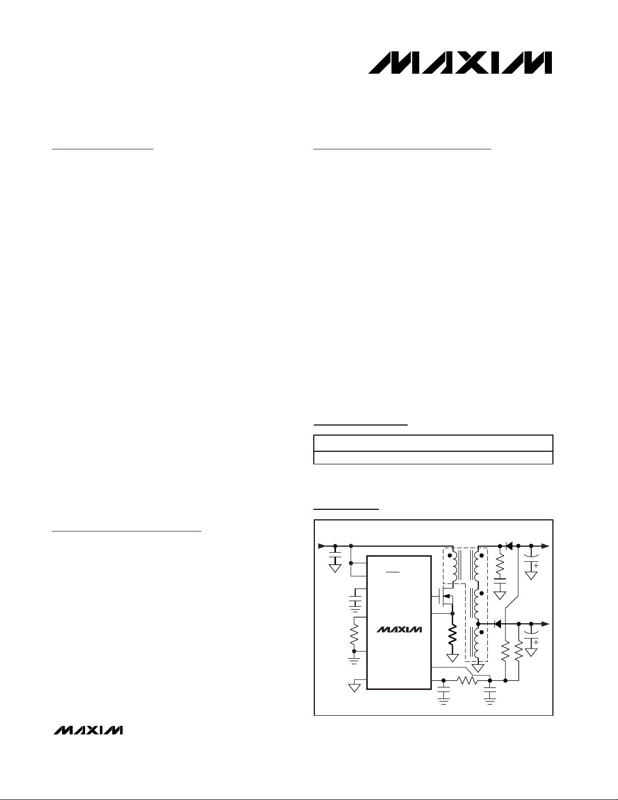
Typical Operating Circuit
Ordering Information
19-1898; Rev 0; 2/01
For price, delivery, and to place orders, please contact Maxim Distribution at 1-888-629-4642,
or visit Maxim’s website at www.maxim-ic.com.
Idle Mode is a trademark of Maxim Integrated Products.
PART TEMP. RANGE PIN-PACKAGE
MAX1856EUB -40°C to +85°C 10 µMAX
INPUT
3V TO 28V
V
CC
SYNC/SHDN
LDO
FREQ
GND
PGND
OUT2
-72V
1
EXT
CS
MAX1856
FB
REF
2
2
2
OUT1
-24V
Page 2
MAX1856
Wide Input Range, Synchronizable,
PWM SLIC Power Supply
2 _______________________________________________________________________________________
ABSOLUTE MAXIMUM RATINGS
ELECTRICAL CHARACTERISTICS
(VCC= SYNC/SHDN, V
CC
= 5V, V
LDO
= 5V, R
OSC
= 200kΩ, TA= 0°C to +85°C. Typical values are at TA= +25°C, unless otherwise noted.)
Stresses beyond those listed under “Absolute Maximum Ratings” may cause permanent damage to the device. These are stress ratings only, and functional
operation of the device at these or any other conditions beyond those indicated in the operational sections of the specifications is not implied. Exposure to
absolute maximum rating conditions for extended periods may affect device reliability.
VCC, SYNC/SHDN to GND .....................................-0.3V to +30V
PGND to GND .......................................................-0.3V to +0.3V
LDO, FREQ, FB, CS to GND.....................................-0.3V to +6V
EXT, REF to GND......................................-0.3V to (V
LDO
+ 0.3V)
LDO Output Current............................................-1mA to +20mA
LDO Short Circuit to GND ...............................................<100ms
REF Short Circuit to GND ...........................................Continuous
Continuous Power Dissipation (T
A
= +70°C)
10-Pin µMAX (derate 5.6mW/°C above +70°C) ...........444mW
Operating Temperature Range ...........................-40°C to +85°C
Junction Temperature......................................................+150°C
Storage Temperature Range .............................-65°C to +150°C
Lead Temperature (soldering, 10s) .................................+300°C
PWM CONTROLLER
Operating Input Voltage Range V
FB Input Current I
Load Regulation VCS = 0 to 100mV for 0 to I
Line Regulation Typically 0.0074% per % duty factor on EXT 0.0074 %/%
Current-Limit Threshold V
CS Input Current I
Idle Mode Current-Sense
Threshold
VCC Supply Current (Note 1) I
Shutdown Supply Current SYNC/SHDN = GND, VCC = 28V 3.5 6 µA
REFERENCE AND LDO REGULATOR
LDO Output Voltage V
Undervoltage Lockout
Threshold
REF to FB Voltage (Note 2) V
REF Load Regulation I
REF Undervoltage Lockout
Threshold
OSCILLATOR
Oscillator Frequency f
Maximum Duty Cycle D
PARAMETER SYMBOL CONDITIONS MIN TYP MAX UNITS
CC
FB
CS
CS
CC
LDO
V
UVLO
REF
OSC
328V
VCC = V
VFB = -0.05V 1 50 nA
CS = GND 1 µA
VFB = -0.05V, VCC = 3V to 28V 250 400 µA
R
V
R
Rising edge, 1% hysteresis (typ) 1.0 1.1 1.2 V
R
R
R
R
R
R
LDO
LOAD(MAX)
= 400Ω
LDO
falling edge, 1% hysteresis (typ) 2.40 2.50 2.60 V
LDO
= 10kΩ, C
REF
= 0 to 400µA -2 -10 mV
REF
= 100kΩ ±1% 425 500 575
OSC
= 200kΩ ±1% 225 250 275
OSC
= 500kΩ ±1% 85 100 115
OSC
= 100kΩ ±1% 86 90 94
OSC
= 200kΩ ±1% 87 90 93
OSC
= 500kΩ ±1% 86 90 94
OSC
5V ≤ VCC ≤ 28V 4.50 5.00 5.50
3V ≤ V
= 0.22µF 1.225 1.250 1.275 V
REF
≤ 28V 2.65 5.50
CC
2.7 5.5 V
0.013 %/mV
85 100 115 mV
51525mV
V
kHz
%
Page 3
MAX1856
Wide Input Range, Synchronizable,
PWM SLIC Power Supply
_______________________________________________________________________________________ 3
ELECTRICAL CHARACTERISTICS (continued)
(VCC= SYNC/SHDN, V
CC
= 5V, V
LDO
= 5V, R
OSC
= 200kΩ, TA= 0°C to +85°C. Typical values are at TA= +25°C, unless otherwise noted.)
ELECTRICAL CHARACTERISTICS
(VCC= SYNC/SHDN, V
CC
= 5V, V
LDO
= 5V, R
OSC
= 200kΩ, TA= -40°C to +85°C, unless otherwise noted.) (Note 3)
Minimum EXT Pulse Width 290 ns
Minimum SYNC Input Signal
Duty Cycle
Minimum SYNC Input
Low Pulse Width
Maximum SYNC Input
Rise/Fall Time
SYNC Input Frequency Range f
SYNC/SHDN Falling Edge to
Shutdown Delay
SYNC/SHDN Input High Voltage V
SYNC/SHDN Input Low Voltage V
SYNC/SHDN Input Current
EXT Sink/Source Current I
EXT On-Resistance R
PARAMETER SYMBOL CONDITIONS MIN TYP MAX UNITS
SYNC
t
SHDN
IH
IL
EXT
ON(EXT)
20 45 %
50 200 ns
200 ns
100 500 kHz
50 µs
2.0 V
0.45 V
V
SYNC/SHDN
V
SYNC/SHDN
EXT forced to 2V 1 A
EXT high or low 2 5 Ω
= 5V 0.5 3.0
= 28V 1.5 10
PWM CONTROLLER
Operating Input Voltage Range V
FB Input Current I
Current-Limit Threshold V
CS Input Current I
V
Shutdown Supply Current SYNC/SHDN = GND, VCC = 28V 6 µA
REFERENCE AND LDO REGULATOR
LDO Output Voltage V
REF to FB Voltage (Note 2) V
REF Load Regulation I
REF Undervoltage Lockout
Threshold
OSCILLATOR
PARAMETER SYMBOL CONDITIONS MIN TYP MAX UNITS
Supply Current (Note 1) I
CC
CC
FB
CS
CS
CC
LDO
REF
OSC
328V
VCC = V
VFB = -0.05V 50 nA
CS = GND 1 µA
VFB = -0.05V, VCC = 3V to 28V 400 µA
R
R
Rising edge, 1% hysteresis (typ) 1.0 1.2 V
R
R
R
LDO
= 400Ω
LDO
= 10kΩ, C
REF
= 0 to 400µA -10 mV
REF
= 100kΩ ±1% 425 575
OSC
= 200kΩ ±1% 222 278Oscillator Frequency f
OSC
= 500kΩ ±1% 85 115
OSC
REF
5V ≤ VCC ≤ 28V 4.50 5.50
3V ≤ V
= 0.22µF 1.22 1.28 V
≤ 28V 2.65 5.50
CC
2.7 5.5 V
85 115 mV
µA
V
kHz
Page 4
MAX1856
Wide Input Range, Synchronizable,
PWM SLIC Power Supply
4 _______________________________________________________________________________________
)
ELECTRICAL CHARACTERISTICS (continued)
(VCC= SYNC/SHDN, V
CC
= 5V, V
LDO
= 5V, R
OSC
= 200kΩ, TA= -40°C to +85°C, unless otherwise noted.) (Note 3)
Note 1: This is the V
CC
current consumed when active, but not switching, so the gate-drive current is not included.
Note 2: The reference output voltage (V
REF
) is measured with respect to FB. The difference between REF and FB is guaranteed to
be within these limits to ensure output voltage accuracy.
Note 3: Specifications to -40°C are guaranteed by design, not production tested.
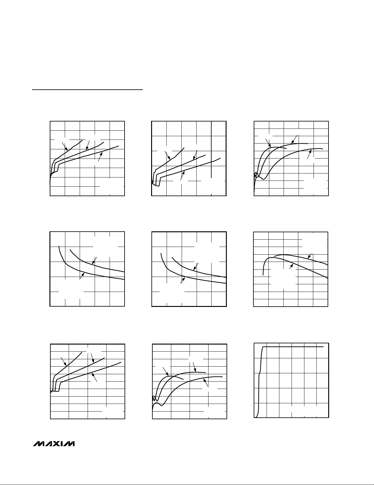
Typical Operating Characteristics
(Circuit of Figure 1, VCC= V
SYNC/SHDN
= 12V, V
OUT1
= -24V, V
OUT2
= -72V, R
OSC
= 200kΩ, unless otherwise noted.)
-24.5
-24.0
-23.0
-23.5
-22.5
-22.0
0 200100 300 400 500 600 700
-24V OUTPUT VOLTAGE
vs. LOAD CURRENT
MAX1856 toc01
I
OUT1
(mA)
V
OUT1
(V)
VIN = 5V
VIN = 12V
VIN = 24V
V
OUT1
= -24V
V
OUT2
= -72V
I
OUT2
= 5mA
-74.5
-74.0
-73.0
-73.5
-72.5
-72.0
0 200100 300 400 500 600 700
-72V CROSS-REGULATION VOLTAGE
vs. LOAD CURRENT
MAX1856 toc02
I
OUT1
(mA)
V
OUT2
(V)
VIN = 5V
VIN = 24V
V
OUT1
= -24V
V
OUT2
= -72V
I
OUT2
= 5mA
VIN = 12V
50
60
70
90
80
100
0 100 200 300 400 500 600 700
EFFICIENCY vs. LOAD CURRENT
(-24V OUTPUT)
MAX1856 toc03
I
OUT1
(mA)
EFFICIENCY (%)
V
OUT1
= -24V
V
OUT2
= -72V
I
OUT2
= 5mA
VIN = 5V
VIN = 24V
VIN = 12V
PARAMETER SYMBOL CONDITIONS MIN TYP MAX UNITS
Minimum SYNC Input Signal
Duty Cycle
Minimum SYNC Input
Low Pulse Width
SYNC Input Frequency Range f
SYNC/SHDN Input High Voltage V
SYNC/SHDN Input Low Voltage V
SYNC/SHDN Input Current
EXT On-Resistance R
SYNC
IH
IL
ON(EXT
R
= 100kΩ ±1% 86 94
OSC
R
= 200kΩ ±1% 87 93Maximum Duty Cycle D
OSC
= 500kΩ ±1% 86 94
R
OSC
V
SYNC/SHDN
V
SYNC/SHDN
= 5V 3.0
= 28V 10
EXT high or low 5 Ω
%
45 %
200 ns
100 500 kHz
2.0 V
0.45 V
µA
Page 5
MAX1856
Wide Input Range, Synchronizable,
PWM SLIC Power Supply
_______________________________________________________________________________________ 5
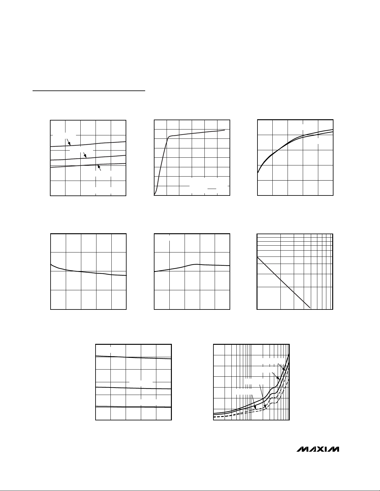
Typical Operating Characteristics (continued)
(Circuit of Figure 1, VCC= V
SYNC/SHDN
= 12V, V
OUT1
= -24V, V
OUT2
= -72V, R
OSC
= 200kΩ, unless otherwise noted.)
-74
-73
-72
-71
-70
0 50 100 150 200 250
-72V OUTPUT VOLTAGE
vs. LOAD CURRENT
MAX1856 toc04
I
OUT2
(mA)
V
OUT2
(V)
V
OUT1
= -24V
V
OUT2
= -72V
I
OUT1
= 5mA
VIN = 5V
VIN = 24V
VIN = 12V
-24.0
-23.8
-23.4
-23.6
-23.2
-23.0
010050 150 200 250
-24V CROSS-REGULATION VOLTAGE
vs. LOAD CURRENT
MAX1856 toc05
I
OUT2
(mA)
V
OUT1
(V)
V
OUT1
= -24V
V
OUT2
= -72V
I
OUT1
= 5mA
VIN = 5V
VIN = 24V
VIN = 12V
50
60
70
80
90
100
010050 150 200 250
EFFICIENCY vs. LOAD CURRENT
(-72V OUTPUT)
MAX1856 toc06
I
OUT2
(mA)
EFFICIENCY (%)
V
OUT1
= -24V
V
OUT2
= -72V
I
OUT1
= 5mA
VIN = 5V
VIN = 24V
VIN = 12V
-24V OUTPUT VOLTAGE
vs. INPUT VOLTAGE
-23.0
V
= -24V
OUT1
= 100mA
I
VIN (V)
V
I
OUT1
OUT2
OUT2
= -72V
= 100mA
-23.2
-23.4
(V)
OUT1
V
-23.6
-23.8
-24.0
V
= -24V
OUT1
= 50mA
I
OUT1
= -72V
V
OUT2
= 50mA
I
OUT2
0105152025
MAX1856 toc07
-72V OUTPUT VOLTAGE
-71.0
-71.4
-71.8
(V)
OUT1
V
-72.2
V
OUT1
= 50mA
I
-72.6
-73.0
OUT1
V
OUT2
= 50mA
I
OUT2
0105152025
vs. INPUT VOLTAGE
V
OUT1
= 100mA
I
OUT1
V
OUT2
= 100mA
I
OUT2
= -24V
= -72V
VIN (V)
100
= -24V
MAX1856 toc08
90
= -72V
80
70
EFFICIENCY (%)
60
50
0105152025
DUAL-OUTPUT EFFICIENCY
vs. INPUT VOLTAGE
V
OUT1
= 100mA
I
OUT1
V
OUT2
= 100mA
I
OUT2
V
= -24V
OUT1
= 50mA
I
OUT1
= -72V
V
OUT2
= 50mA
I
OUT2
VIN (V)
= -24V
= -72V
MAX1856 toc09
-48V OUTPUT VOLTAGE
-46.5
VIN = 5V
-46.9
-47.3
(V)
OUT2
V
-47.7
-48.1
-48.5
0 100 200 300 400
SUPPLY CURRENT
vs. INPUT VOLTAGE
vs. LOAD CURRENT
EFFICIENCY vs. LOAD CURRENT
(-48V OUTPUT)
100
250
VIN = 12V
MAX1856 toc10
90
VIN = 12V
MAX1856 toc11
200
VIN = 5V
80
150
VIN = 24V
70
EFFICIENCY (%)
V
= -48V
OUT
FIGURE 4
I
(mA)
OUT2
60
50
0 100 200 300 400
I
OUT2
(mA)
VIN = 24V
V
OUT
FIGURE 4
= -48V
100
SUPPLY CURRENT (µA)
50
CURRENT INTO VCC PIN
R
0
0105 15202530
OSC
INPUT VOLTAGE (V)
MAX1856 toc12
= 500kΩ
Page 6
MAX1856
Wide Input Range, Synchronizable,
PWM SLIC Power Supply
6 _______________________________________________________________________________________
Typical Operating Characteristics (continued)
(Circuit of Figure 1, VCC= V
SYNC/SHDN
= 12V, V
OUT1
= -24V, V
OUT2
= -72V, R
OSC
= 200kΩ, unless otherwise noted.)
1.240
1.250
1.245
1.255
1.260
REFERENCE VOLTAGE
vs. REFERENCE CURRENT
MAX1856 toc16
REFERENCE CURRENT (µA)
V
REF
(V)
0 200100 300 500
400
1.240
1.250
1.245
1.255
1.260
REFERENCE VOLTAGE
vs. TEMPERATURE
MAX1856 toc17
TEMPERATURE (°C)
V
REF
(V)
-40 10-15 35 85
60
NO LOAD
1000
100
100 1000
SWITCHING FREQUENCY vs. R
OSC
MAX1856 toc18
R
OSC
(kΩ)
SWITCHING FREQUENCY (kHz)
0
200
100
400
300
500
600
-40 10-15 35 60 85
SWITCHING FREQUENCY
vs. TEMPERATURE
MAX1856 toc19
TEMPERATURE (°C)
SWITCHING FREQUENCY (kHz)
R
OSC
= 100kΩ
R
OSC
= 200kΩ
R
OSC
= 500kΩ
70
0
0.1 1 10
EXT RISE/FALL TIME
vs. CAPACITANCE
10
MAX1856 toc20
CAPACITANCE (nF)
EXT RISE/FALL TIME (ns)
30
50
60
40
20
t
RISE
, VIN = 5V
t
RISE
, VIN = 3.3V
t
FALL
, VIN = 5V
t
FALL
, VIN = 3.3V
150
190
270
230
310
350
-40 10-15 35 60 85
SUPPLY CURRENT
vs. TEMPERATURE
MAX1856 toc13
TEMPERATURE (°C)
SUPPLY CURRENT (µA)
R
OSC
= 100kΩ
R
OSC
= 200kΩ
R
OSC
= 500kΩ
CURRENT INTO VCC PIN
0
0.5
1.0
1.5
2.0
2.5
3.0
3.5
4.0
0105 15202530
SHUTDOWN CURRENT
vs. INPUT VOLTAGE
MAX1856 toc14
INPUT VOLTAGE (V)
SHUTDOWN CURRENT (µA)
CURRENT INTO VCC PIN
R
OSC
= 500kΩ
SYNC/SHDN = GND
0
50
150
100
200
250
0426810
LDO DROPOUT VOLTAGE
vs. LOAD CURRENT
MAX1856 toc15
I
LDO
(mA)
DROPOUT VOLTAGE (V)
VIN = 5V
VIN = 3.3V
Page 7

A. V
OUT
= -48V, I
OUT
= 200mA, 50mV/div
B. I
LP
, 2A/div
CIRCUIT OF FIGURE 4
HEAVY-LOAD SWITCHING WAVEFORM
MAX1856 toc23
-47.2V
-47.0V
-47.1V
2A
0
2.0µs/div
A
B
4A
A. V
OUT
= -48V, I
OUT
= 20mA, 20mV/div
B. I
LP
, 2A/div
CIRCUIT OF FIGURE 4
LIGHT-LOAD SWITCHING WAVEFORM
MAX1856 toc24
-47.80V
-47.72V
-47.76V
2A
0
4µs/div
A
B
MAX1856
Wide Input Range, Synchronizable,
PWM SLIC Power Supply
_______________________________________________________________________________________ 7
Typical Operating Characteristics (continued)
(Circuit of Figure 1, VCC= V
SYNC/SHDN
= 12V, V
OUT1
= -24V, V
OUT2
= -72V, R
OSC
= 200kΩ, unless otherwise noted.)
EXITING SHUTDOWN
5V
0
2A
0
0
-20V
-40V
-60V
A. V
SYNC/SHDN
, 2A/div
B. I
LP
C. V
OUT
CIRCUIT OF FIGURE 4
= -48V, R
4ms/div
= 0 TO 5V, 5V/div
= 2.4kΩ, 20V/div
OUT
MAX1856 toc21
A
B
C
5V
0
5V
0
2A
0
200mA
0
-47.1V
-47.6V
-48.1V
ENTERING SHUTDOWN
A. V
B. V
C. I
V
OUT
CIRCUIT OF FIGURE 4
SYNC/SHDN
, 5V/div
EXT
, 2A/div
LP
= -48V, R
= 5V TO 0, 5V/div
= 240Ω
OUT
LOAD TRANSIENT
10µs/div
MAX1856 toc22
MAX1856 toc25
A
B
C
A
B
C
14V
12V
10V
-47V
LINE TRANSIENT
MAX1856 toc26
A
B
A. I
= 20mA TO 200mA, 200mA/div
OUT
, = -48V, 500mV/div
B. V
OUT
, 2A/div
C. I
LP
CIRCUIT OF FIGURE 4
1ms/div
A. V
= 10V TO 14V, 2Vdiv
IN
= -48V, I
B. V
OUT
CIRCUIT OF FIGURE 4
400µs/div
= 200mA, 100mV/div
OUT
RINGER TO TALK-BATTERY CROSSTALK
60
RINGER OUTPUT
MAX1856 toc27
TALK-BATTERY OUTPUT
FREQUENCY (Hz)
40
20
0
-20
(dB)
-40
-60
-80
-100
0 50 100 150 200 250
Page 8
MAX1856
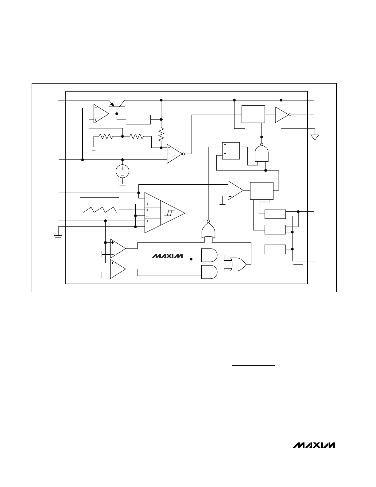
Detailed Description
The MAX1856 current-mode PWM controller uses an
inverting flyback configuration that is ideal for generating the high negative voltages required for SLIC power
supplies. Optimum conversion efficiency is maintained
over a wide range of loads by employing both PWM
operation and Maxim’s proprietary Idle Mode control to
minimize operating current at light loads. Other features
include shutdown, adjustable internal operating frequency or synchronization to an external clock, softstart, adjustable current limit, and a wide (3V to 28V)
input range.
PWM Controller
The heart of the MAX1856 current-mode PWM controller is a BiCMOS multi-input comparator that simultaneously processes the output-error signal, the
current-sense signal, and a slope-compensation ramp
(Figure 2). The main PWM comparator is direct summing, lacking a traditional error amplifier and its associ-
ated phase shift. The direct-summing configuration
approaches ideal cycle-by-cycle control over the output voltage since there is no conventional error amplifier in the feedback path.
In PWM mode, the controller uses fixed-frequency, current-mode operation where the duty ratio is set by the
input-to-output voltage ratio and the transformer’s turn
ratio. The current-mode feedback loop regulates peak
inductor current as a function of the output error signal.
At light loads, the controller enters Idle Mode. During
Idle Mode, switching pulses are provided only as necessary to supply the load, and operating current is minimized to provide the best light-load efficiency. The
minimum-current comparator threshold is 15mV, or
15% of the full-load value (I
MAX
) of 100mV. When the
controller is synchronized to an external clock, Idle
Mode occurs only at very light loads.
Wide Input Range, Synchronizable,
PWM SLIC Power Supply
8 _______________________________________________________________________________________
Pin Description
PIN NAME FUNCTION
1LDO
2 FREQ
3 GND Analog Ground
4 REF 1.25V Reference Output. REF can source up to 400µA. Bypass to GND with a 2.2µF ceramic capacitor.
5 FB Feedback Input. The feedback voltage threshold is 0.
6 CS Positive Current-Sense Input. Connect a current-sense resistor (RCS) between CS and PGND.
7 PGND Power Ground
8 EXT External MOSFET Gate-Driver Output. EXT swings from LDO to PGND.
9V
10 SYNC/SHDN
CC
5V Linear Regulator Output. The regulator powers all of the internal circuitry, including the EXT gate
driver. Bypass LDO to GND with a 1µF or greater ceramic capacitor.
OSC
OSC
when
=
Oscillator Frequency Set Input. A resistor from FREQ to GND sets the oscillator from 100kHz (R
500kΩ) to 500kHz (R
an external clock is connected to SYNC/SHDN.
Input Supply to the Linear Regulator. VCC accepts inputs up to 28V. Bypass to PGND with a 1µF
ceramic capacitor.
Shutdown Control and Synchronization Input. There are three operating modes:
• SYNC/SHDN low: shutdown mode
• SYNC/SHDN high: the DC-to-DC controller operates with the oscillator frequency set at FREQ by
R
OSC
• SYNC/SHDN clocked: the DC-to-DC controller operates with the oscillator frequency set by the SYNC
clock input. The conversion cycles initiate on the rising edge of the input clock signal. However, the
MAX1856 still requires R
= 100kΩ): f
OSC
= 50MΩ-kHz / R
OSC
when SYNC/SHDN is externally clocked.
OSC
. The MAX1856 still requires R
OSC
Page 9

Low-Dropout Regulator (LDO)
All MAX1856 functions, including EXT, are internally
powered from the on-chip, low-dropout 5V regulator.
The regulator input is at VCC, while its output is at LDO.
The VCC-to-LDO dropout voltage is typically 200mV
(300mV max at 12mA), so that when VCCis <5.2V,
V
LDO
is typically VCC- 200mV. When the LDO is in
dropout, the MAX1856 still operates with VCCas low as
3V (as long as the LDO exceeds 2.7V), but with
reduced amplitude FET drive at EXT. The maximum
VCCinput voltage is 28V.
LDO can supply up to 12mA to power the IC, supply
gate charge through EXT to the external FET, and supply small external loads. When driving particularly large
FETs at high switching rates, little or no LDO current
may be available for external loads. For example, when
switched at 500kHz, a large FET with 20nC gate charge
requires 20nC ✕500kHz, or 10mA.
Soft-Start
The MAX1856 features a “digital” soft-start that is preset and requires no external capacitor. Upon startup,
the peak inductor current increments from 1/5th of the
value set by RCS, to the full current-limit value in five
steps over 1024 cycles of f
OSC
or f
SYNC
. Additionally,
the oscillator runs at 1/3 the normal operating frequency (f
OSC
/3) until the output voltage reaches 20% of its
nominal value (V
FB
≤ 1.0V). See the Typical Operating
Characteristics for a scope picture of the soft-start
operation. Soft-start is implemented: 1) when power is
first applied to the IC, 2) when exiting shutdown with
power already applied, and 3) when exiting undervoltage lockout. The MAX1856’s soft-start sequence does
not start until V
LDO
reaches 2.5V.
Design Procedure
The MAX1856 can operate within a wide input voltage
range from 3V to 28V. This allows it to be used with wall
adapters. In applications driven by low-power, low-cost
and low input and output ripple current requirements,
the MAX1856 flyback topology can be used to generate various levels of output voltages and multiple outputs.
Communications over the Internet interface with a standard telephone connection, which includes the
Subscriber Line Interface Circuit (SLIC). The SLIC
requires a negative power supply for the audio and
ringer functions. The circuits discussed here are
designed for these applications. The following design
discussions are related to the standard application cir-
MAX1856
Wide Input Range, Synchronizable,
PWM SLIC Power Supply
_______________________________________________________________________________________ 9
Figure 1. Standard Application Circuit
*INPUT
4.5V TO 24V
*INPUT RANGE LIMITED BY OUTPUT POWER REQUIREMENTS.
SEE MAXIMUM OUTPUT POWER AND TYPICAL OPERATING CHARACTERISTICS.
10Ω
C4
1µF
C
LDO
1µF
R
OSC
200kΩ
R5
9
V
10
SYNC/SHDN
1
LDO
2
FREQ
3
GND
7
PGND
CC
MAX1856
C
(2x) 10µF
25V
8
EXT
6
CS
5
FB
4
REF
IN
R6
100Ω
C5
1nF
R3
5.11kΩ
C
REF
2.2µF
T1
1
M1
R
CS
33mΩ
C
FB
1nF
D1, D2: Central Semiconductor CMR1U-02
M1: International Rectifier IRLL2705
T1: Coiltronics CTX01-14853
D2
2
2
D1
2
R2
681kΩ
R4
470Ω
C3
100pF
R1
174kΩ
OUT2
-72V
C2
100µF
Sanyo
100MV100AX
OUT1
-24V
C1
330µF
Sanyo
35MV330AX
Page 10
MAX1856
Wide Input Range, Synchronizable,
PWM SLIC Power Supply
10 ______________________________________________________________________________________
cuit (Figure 1) converting a +12V input to a -72V output
(maximum load 100mA) and a -24V output (maximum
load 400mA).
Maximum Output Power
The maximum output power the MAX1856 can provide
depends on the maximum input power available and
the circuit’s efficiency:
Furthermore, the efficiency and input power are both
functions of component selection. Efficiency losses can
be divided into three categories: 1) resistive losses
across the transformer, MOSFET’s on-resistance, current-sense resistor, and the ESR of the input and output
capacitors; 2) switching losses due to the MOSFET’s
transition region, the snubber circuit, which also
increases the transition times, and charging the MOSFET’s gate capacitance; and 3) transformer core loss-
es. Typically, 80% efficiency can be assumed for initial
calculations. The input power depends on the current
limit, input voltage, output voltage, inductor value, the
transformer’s turns ratio, and the switching frequency:
where N
P:NS
is the transformer’s turns ratio.
Setting the Operating Frequency
(SYNC/SHDN and FREQ)
The SYNC/SHDN pin provides both external-clock synchronization (if desired) and shutdown control. When
SYNC/SHDN is low, all IC functions are shut down. A
logic high at SYNC/SHDN selects operation at a
Figure 2. Functional Diagram
V
9
CC
REF
4
5
FB
6
CS
3
GND
R3
276kΩ
SLOPE COMP
100mV
15mV
ANTISAT
R2
276kΩ
V
REF
1.25V
I
I
MAX
MIN
X6
X1
X1
MAX1856
R1
552kΩ
1.0V
LDO
1
MUX
01
R
Q
S
MUX
1
0
F
OSC
F
/3
OSC
BIAS
EXT
PGND
FREQ
SYNC/SHDN
8
7
2
10
P EFFICIENCY P
OUT MAX IN MAX() ()
=×
PVD
IN MAX IN
()
NV
=
D
NV NV
P OUT S IN
V
CS
=−
R
CS
P OUT
+
VD
ƒ
2
IN
OSC
L
Page 11

MAX1856
Wide Input Range, Synchronizable,
PWM SLIC Power Supply
______________________________________________________________________________________ 11
100kHz to 500kHz frequency, which is set by a resistor
(R
OSC
) connected from FREQ to GND. The relationship
between f
OSC
and R
OSC
is:
Thus, a 250kHz operating frequency, for example, is
set with R
OSC
= 200kΩ. At higher frequencies, the
magnetic components will be smaller. Peak currents
and, consequently, resistive losses will be lower at the
higher switching frequency. However, core losses, gate
charge currents, and switching losses increase with
higher switching frequencies.
Rising clock edges on SYNC/SHDN are interpreted as
synchronization input. If the sync signal is lost while
SYNC/SHDN is high, the internal oscillator takes over at
the end of the last cycle, and the frequency is returned
to the rate set by R
OSC
. If the signal is lost with
SYNC/SHDN low, the IC waits for 50µs before shutting
down. This maintains output regulation even with intermittent sync signals. When an external sync signal is
used, Idle Mode switchover at the 15mV current-sense
threshold is disabled so that Idle Mode only occurs at
very light loads. Also, R
OSC
should be set for a fre-
quency 15% below the SYNC clock rate:
Setting the Output Voltage
Set the output voltage using two external resistors forming a resistive divider to FB between the output and
REF. First select a value for R3 between 3.3kΩ and
100kΩ. R1 is then given by:
For a dual output as shown in Figure 1, a split feedback
technique is recommended. Since the feedback voltage threshold is 0, the total feedback current is:
Since the feedback resistors are connected to the reference, I
TOTAL
must be <400µA so that V
REF
is guaranteed to be in regulation (see Electrical Characteristics
Table). Therefore, select R3 so the total current value is
between 200µA and 250µA as shown in Figure 1. To
ensure that the MAX1856 regulates both outputs with
the same degree of accuracy over load, select the
feedback resistors (R1 and R2) so their current ratio
(I
R1:IR2
) equals the output power ratio (P
OUT1:POUT2
)
under full load:
Once R3 and the dual feedback currents (I
R1
and IR2)
are determined from the two equations above, use the
following two equations to determine R1 and R2:
Selecting the Transformer
The MAX1856 PWM controller works with economical
off-the-shelf transformers. The transformer selection
depends on the input-to-output voltage ratio, output
current capacity, duty cycle, and oscillator frequency.
Table 1 shows recommended transformers for the typical applications, and Table 2 gives some recommended suppliers.
Transformer Turns Ratio
The transformer turns ratio is a function of the input-tooutput voltage ratio and maximum duty cycle. Under
steady-state conditions, the change in flux density during the on-time must equal the return change in flux
density during the off-time (or flyback period):
For example, selecting a 50% duty cycle for the standard application circuit (Figure 1) and a +12V input
voltage, the -72V output requires a 1:6 turns ratio, and
the -24V output requires a 1:2 turns ratio. Therefore, a
transformer with a 1:2:2:2 turns ratio was selected.
Primary inductance
The average input current at maximum load can be calculated as:
where η = efficiency. For V
OUT
= -24V, I
OUT(MAX)
=
400mA, and V
IN(MIN)
= 10.8V as shown in Figure 1, this
R
OSC
=
M kHz
50 Ω
ƒ
OSC
×
kHz
()
R
OSC SYNC
()
M kHz
×
50
=
Ω
ƒ
OSC
kHz
.()
085
RR
13=
V
OUT
V
REF
III
=+=
TOTAL R R
12
V
REF
3
R
VI
I
OUT OUT
R
1
=
I
VI
R
OUT OUT
2
11
22
V
OUT
I
==
R
1
12
R
1
and I
V
OUT
R
2
2
R
VtNVt
IN ONPOUT OFF
=
N
S
I
IN DC
VI
=
()
OUT OUT MAX
η
V
IN MIN
()
()
Page 12
MAX1856
Wide Input Range, Synchronizable,
PWM SLIC Power Supply
12 ______________________________________________________________________________________
gives 1.11A for 80% efficiency. With a duty cycle of
52.5%, the average switch current (I
SW(AVG)
) is 2.114A.
Choosing a primary inductance ripple current ∆ILto be
40% of the average switch current, the primary inductance is given by:
Selecting f
OSC
= 250kHz and ∆IL= 0.4 x I
SW(AVG)
=
0.846A, the primary inductance value is 27µH, and the
peak primary current for this example is therefore 2.5A.
Core Selection
The transformer in a flyback converter is a coupled
inductor with multiple windings on the same magnetic
core. Flyback topologies operate by storing energy in
the transformer magnetics during the on-time and
transferring this energy to the output during the offtime.
Core selection depends on the core’s power-handling
capability. The required output power is first considered. For example, the standard application circuit
requires 9.6W. Assuming a typical 80% efficiency, the
transformer must support 12W of power. The core
material’s properties, the core’s shape, and the size of
the air gap determine the core’s power rating. Since the
equations relating these properties to the power capability are involved, manufacturers simply provide charts
giving “Power vs. Frequency” for different core sizes.
For the standard application circuit (f
OSC
= 250kHz),
the EFD15 core from Coiltronics meets the criteria.
Once the core is chosen, the number of turns in the primary is given by:
where A
L
is the inductance factor. Ensure that the num-
ber of ampere-turns (NPI
SAT
) is below the saturation
limit. A significant portion of the total energy is stored in
the air gap. Therefore, the larger the air gap, the lower
the ALvalue and the larger the number of ampere-turns
at which saturation starts. Some manufacturers define
saturation as the current at which the inductance
decreases by 30%.
Current-Sense Resistor Selection
Once the peak inductor current is determined, the current-sense resistor (RCS) is determined by:
Kelvin-sensing should be used to connect CS and
PGND to R
CS
. Connect PGND and GND together at the
ground side of RCS.
Due to inductive ringing after the MOSFET turns on, a
lowpass filter may be required between R
CS
and CS to
prevent the noise from tripping the current-sense comparator. Connect a 100Ω resistor between CS and the
Table 1. Transformer Selection for Standard Applications
Table 2. Transformer Suppliers
INPUT VOLTS (V) OUTPUT VOLTS (V) OUTPUT CURRENT (mA) TRANSFORMER (VENDOR)
5 -48 100 VP3-0055 (Coiltronics)
12 -48 100
12 -24 and -72 400 or 100
12 -95 and -30 320 and 150 CTX03-15220 (Coiltronics)
CTX01-14853 (Coiltronics), or
ICA-0635 (ICE Components)
CTX01-14853 (Coiltronics), or
ICA-0635 (ICE Components)
Coilcraft 847-639-6400 847-639-1469 www.coilcraft.com
Coiltronics 888-414-2645 561-241-9339 www.coiltronics.com
ICE Components 800-729-2099 703-257-7547 www.icecomponents.com
Pulse Engineering 858-674-8100 858-674-8262 www.pulseeng.com
TDK 847-390-4461 847-390-4405 www.tdk.com
VENDOR USA PHONE USA FAX INTERNET
VD
P
=
∆ƒ
IN
I
L OSC
L
L
N
P
=
P
A
L
V
CS MIN
R
CS
()
==
I
LPEAK
mV I
/85
LPEAK
Page 13

MAX1856
Wide Input Range, Synchronizable,
PWM SLIC Power Supply
______________________________________________________________________________________ 13
high side of RCS, and connect a 1000pF capacitor
between CS and GND.
Power MOSFET Selection
The MAX1856 drives a wide variety of N-channel power
MOSFETs (NFETs). Since the LDO limits the EXT output
gate drive to no more than 5V, a logic-level NFET is
required. Best performance, especially with input voltages below 5V, is achieved with low-threshold NFETs
that specify on-resistance with a gate-to-source voltage
(VGS) of 2.7V or less. When selecting an NFET, key
parameters include:
1) Total gate charge (Q
G
)
2) Reverse transfer capacitance or charge (C
RSS
)
3) On-resistance (R
DS(ON)
)
4) Maximum drain-to-source voltage (V
DS(MAX)
)
5) Minimum threshold voltage (V
TH(MIN)
)
At high switching rates, dynamic characteristics (parameters 1 and 2 above) that predict switching losses
may have more impact on efficiency than R
DS(ON)
,
which predicts DC losses. QGincludes all capacitance
associated with charging the gate. In addition, this
parameter helps predict the current needed to drive the
gate at the selected operating frequency. The continuous LDO current for the FET gate is:
For example, the IRLL2705 has a typical Q
G
of 17nC
(at VGS= 5V); therefore, the I
GATE
current at 500kHz is
8.5mA.
The switching element in a flyback converter must have
a high enough voltage rating to handle the input voltage plus the reflected secondary voltage, as well as
any spikes induced by leakage inductance. The reflected secondary voltage is given by:
where V
DIODE
is the voltage drop across the output
diode. For a 10% variation in input voltage and a 30%
safety margin, this gives a required 33V voltage rating
(VDS) for the switching MOSFET in Figure 1. The
IRLL2705 with a VDSof 55V was chosen.
Diode Selection
The MAX1856’s high switching frequency demands a
high-speed rectifier. Schottky diodes are recommended for most applications because of their fast recovery
time and low forward voltage. Ensure that the diode’s
average current rating exceeds the peak secondary
current, using the diode manufacturer’s data or approximating it with the following formula:
where N = N
s/NP
is the secondary-to-primary turns
ratio. Additionally, the diode’s reverse breakdown voltage must exceed V
OUT
plus the reflected input voltage
plus the leakage inductance spike. For high output voltages (50V or above), Schottky diodes may not be practical because of this voltage requirement. In these
cases, use a faster ultra-fast recovery diode with adequate reverse-breakdown voltage.
Capacitor Selection
Output Filter Capacitor
The output capacitor (C
OUT
) does all the filtering in a fly-
back converter. Typically, C
OUT
must be chosen based
on the output ripple requirement. The output ripple is
due to the variations in the charge stored in the output
capacitor with each pulse and the voltage drop across
the capacitor’s equivalent series resistance (ESR)
caused by the current into and out of the capacitor. The
ESR-induced ripple usually dominates, so output capacitor selection is actually based upon the capacitor’s
ESR, voltage rating, and ripple current rating.
Input Filter Capacitor
The input capacitor (CIN) in flyback designs reduces
the current peaks drawn from the input supply and
reduces noise injection. The value of CINis largely
determined by the source impedance of the input supply. High source impedance requires high input capacitance, particularly as the input voltage falls. Since
inverting flyback converters act as “constant-power”
loads to their input supply, input current rises as the
input voltage falls. Consequently, in low-input-voltage
designs, increasing C
IN
and/or lowering its ESR can
add as much as 5% to the conversion efficiency.
Bypass Capacitors
In addition to C
IN
and C
OUT
, three ceramic bypass
capacitors are also required with the MAX1856. Bypass
REF to GND with 2.2µF or more. Bypass LDO to GND
with 1µF or more. And bypass VCCto GND with 1µF or
more. All bypass capacitors should be located as close
to their respective pins as possible.
Compensation Capacitor
Output ripple voltage due to C
OUT
ESR affects loop
stability by introducing a left half-plane zero. A small
capacitor connected from FB to GND forms a pole with
IQ
GATE G OSC
=׃
II
D PK OUT
()
=+
1
NV
V
OUT
×
IN
∆
I
L
+
2
N
V
REFLECT
N
P
=+
VV
()
N
S
OUT DIODE
Page 14

MAX1856
Wide Input Range, Synchronizable,
PWM SLIC Power Supply
14 ______________________________________________________________________________________
the feedback resistance that cancels the ESR zero. The
optimum compensation value is:
where R1 and R3 are feedback resistors (Figure 3). If
the calculated value for C
FB
results in a nonstandard
capacitance value, values from 0.5CFBto 1.5CFBwill
also provide sufficient compensation.
Snubber Design
The MAX1856 uses a current-mode controller that
employs a current-sense resistor. Immediately after
turn-on, the MAX1856 uses a 100ns current-sense
blanking period to minimize noise sensitivity. However,
when the MOSFET turns on, the secondary inductance
and the output diode’s parasitic capacitance form a
resonant circuit that causes ringing. Reflected back
through the transformer to the primary side, these oscillations appear across the current-sense resistor and
last well beyond the 100ns blanking period. As shown
in Figure 1, a series RC snubber circuit at the output
diode increases the damping factor, allowing the ringing to settle quickly. Applications with dual output voltages require only one snubber circuit on the higher
voltage output.
The diode’s parasitic capacitance can be estimated
using the diode’s reverse voltage rating (V
RRM
), current
capability (IO), and recovery time (tRR). A rough
approximation is:
For the CMR1U-02 Central Semiconductor diode used
in Figure 1, the capacitance is roughly 172pF. A value
less than this (100pF) was chosen since the output
snubber only needs to dampen the ringing, so the initial
turn-on spike that occurs during the 100ns blanking
period is still present. Larger capacitance values
require more charge, thereby increasing the power dissipation.
The snubber’s time constant (t
SNUB
) must be smaller
than the 100ns blanking time. A typical RC time constant of 50ns was chosen for Figure 1:
When a MOSFET with a transformer load is turned off,
the drain will fly to a high voltage as a result of the energy stored in the transformer’s leakage inductance.
During the switch on-time, current is established in the
leakage inductance (L
L
) equal to the peak primary cur-
rent (I
PEAK
). The energy stored in the leakage induc-
tance is:
When the switch turns off, this energy is transferred to
the MOSFET’s parasitic capacitance, causing a voltage
spike at the MOSFET’s drain. For the IRLL2705 MOSFET, the capacitance value (C
DS
) is 130pF. If all of the
leakage inductance energy transfers to this capacitance, the drain would fly up to:
The leakage inductance is (worst case) 1% of the primary inductance value. For a 0.27µH leakage inductance and a 2.5A peak current, the voltage reaches
114V at the MOSFET’s drain, which is much higher than
the MOSFET’s rated breakdown voltage. This causes
the parasitic bipolar transistor to turn on if the dv/dt at
the drain is high enough. Note that the inductive spike
adds on to the sum of the input voltage and the reflected secondary voltage already present at the drain of
the transistor (see Power MOSFET Selection).
A series combination RC snubber (R7 and C6 in Figure
3) across the MOSFET (drain to source) reduces this
spike. The energy stored in the leakage inductance
transfers to the snubber capacitor (C6) as electrostatic
energy. Therefore, C6 must be large enough to guarantee the voltage spike will not exceed the breakdown
voltage, but not so large as to result in excessive power
dissipation:
Typically, a 30% safety margin is chosen so that V
C6
is
at most equal to about 70% of the MOSFET’s VDSrating. For example, the V
DSS
is 55V for the IRLL2705, so
this gives a value of 1000pF for C9. The amount of
energy stored in snubber capacitor C6 has to discharge through series resistor R7 in the snubber network. During turn-off, the drain voltage rises in a time
period (tf) characteristic of the MOSFET used, which is
22ns for the IRLL2705. The RC time constant should
therefore equal this time. Hence:
1
CC
=
FB OUT
21313( )/( )
ESR
COUT
×+
RR RR
C
DIODE
=
It
ORR
V
RRM
t
SNUB
R
4
==
C
50
ns
3
3
C
L PEAK
2
2
LI
E
=
L
V
COSS
LI
=
L PEAK
C
DS
2
LI
C
6
=
L PEAK
2
V
6
C
2
Page 15

MAX1856
Wide Input Range, Synchronizable,
PWM SLIC Power Supply
______________________________________________________________________________________ 15
This gives a value of about 22Ω for R7. However, this
snubber adds capacity to the MOSFET output, and this
in turn increases the dissipation in the MOSFET during
turn-on.
The selection of the input and output snubbers is an
interactive process. The design procedures above provide initial component recommendations, but the actual
values depend on the layout and transformer winding
practices used in the actual application.
Applications Information
Voice-over-IP CPE systems have +5V or +12V available
from which the talk battery voltage and the ringer voltage must be generated. The examples given below are
circuits using these supply voltages to generate the
negative power supplies needed in such applications.
Low Input Voltage
IP phones and routers require -48V. For cost-sensitive
applications, this needs to be used from an available
+5V supply. The circuit in Figure 4 is an example of
such a circuit using an off-the-shelf transformer from
Coiltronics and ICE components.
SLIC Power Supply with Split Feedback
Telephones in broadband systems use low-power-consuming SLICs that reduce the power drain by providing
the option of using two voltages for loop supervision.
The load on each output is dependent on the number
of lines on- or off-hook. The higher voltage is used to
generate ring battery voltage when the subscriber is onhook, while a second lower voltage is used to generate
talk battery voltage when off-hook is detected. The actual value of these two voltages can be adjusted based on
system requirements and the specific SLIC used. The
design given here specifically addresses the supply
requirements for the AMD79R79 SLIC device with onchip ringing. The input voltage is 12V nominal, and the
output voltages are -24V at 400mA and -72V at 100mA.
The transformer turns ratio is 1:2:2:2, where 24V appears
across each secondary winding. The -72V output is
derived from the -24V output by stacking the secondary
windings in series as shown in Figure 1. A split feedback
is used, using resistors R1, R2, and R3. This allows for
accurate regulation of both outputs (see Typical
Operating Characteristics).
Figure 3. Feedback Compensation and Snubber Circuits
INPUT
3V TO 28V
R5
9
V
CC
10
C4
C
LDO
R
OSC
t
ƒ
R
=
C76
SYNC/SHDN
1
LDO
2
FREQ
3
GND
7
PGND
MAX1856
EXT
CS
FB
REF
C
IN
M1
8
R6
6
C5
5
R3
4
C
REF
T1
R7
C6
R
CS
C
FB
D1
R4
C3
R1
OUTPUT
C1
Page 16

MAX1856
Wide Input Range, Synchronizable,
PWM SLIC Power Supply
16 ______________________________________________________________________________________
Figure 4. -48V Output Application Circuit
INPUT
4.5V TO 24V
10Ω
C4
1µF
C
LDO
1µF
R
OSC
200kΩ
C
R5
9
V
CC
10
SYNC/SHDN
MAX1856
1
LDO
2
FREQ
3
GND
7
PGND
(2x) 10µF
25V
EXT
CS
FB
REF
IN
8
R6
100Ω
6
C5
1nF
5
R3
8.66kΩ
4
C
REF
2.2µF
T1
1
4
M1
R
CS
33mΩ
C
FB
1nF
D1: Central Semiconductor CMR1U-02
M1: International Rectifier IRLL2705
T1: ICE Components ICA-0635
D1
R4
220Ω
C3
330pF
R1
332kΩ
OUTPUT
-48V
C1
100µF
Sanyo
100MV100AX
Page 17

MAX1856
Wide Input Range, Synchronizable,
PWM SLIC Power Supply
______________________________________________________________________________________ 17
Pin Configuration
Chip Information
TRANSISTOR COUNT: 1538
PROCESS: BiCMOS
TOP VIEW
LDO
FREQ
GND
1
2
MAX1856
3
4
5
µMAX
10
9
8
7
6
SYNC/SHDN
V
CC
EXT
PGNDREF
CSFB
Page 18

MAX1856
Wide Input Range, Synchronizable,
PWM SLIC Power Supply
Maxim cannot assume responsibility for use of any circuitry other than circuitry entirely embodied in a Maxim product. No circuit patent licenses are
implied. Maxim reserves the right to change the circuitry and specifications without notice at any time.
Maxim Integrated Products, 120 San Gabriel Drive, Sunnyvale, CA 94086 408-737-7600 ____________________ 18
© 2001 Maxim Integrated Products Printed USA is a registered trademark of Maxim Integrated Products.
Package Information
10LUMAX.EPS
 Loading...